

®
www.BDTIC.com/Intersil
ISL5586
Data Sheet November 3, 2004
Low Power Ringing SLIC for Home
Gateways
The ISL5586 is a very low
power Ringing Subscriber
Interface circuit designed for
use with the Broadcom
BCM3352 Cable Modem Chip,
with on-board voiceband codecs, or other 3.3V voiceband
codec devices.
The ISL5586 provides on board ringing signal generation up
to 95V peak supporting sinusoidal or trapezoidal
waveshapes with DC offset. Loop start and ground start
trunks are supported, and an open circuit DC voltage of less
than 56V is maintained on the subscriber loop in the on-hook
condition, in compliance with MTU operation and the safety
requirements of UL-1950.
Together with the Broadcom BCM3352, the ISL5586
provides resistive and complex two wire impedance
matching and transhybrid balancing. Also supported are onhook transmission of caller id signals, soft and hard polarity
reversal and 12/16kHz subscriber pulse metering systems
used in Europe and Asia, thereby allowing a low cost, low
risk, global product design to be achieved.
Related Literature
• Evaluation Board for the ISL5586 family AN9918
• Technical Brief TB363 “Guidelines for Handling and
Processing Moisture Sensitive Surface Mount Devices
(SMDs)”
FN4924.2
Features
• Interfaces to Broadcom 3352 cable modem device
• Very low on-hook power consumption
- 64mW @ Vbh = 75V
• User Programmable constant current to the subscriber
loop
• On Chip ring generation
- Balanced to 95Vpk
• Sinewave, Trapezoid, DC offset
• Programmable loop start and ring trip detectors
• Loop start, Ground Start, Polarity Reversal (soft/hard)
• On-Hook transmission and pulse metering support
• Integrated battery switch
• Open circuit line voltage clamp
• Compatible with 3.3V devices
• TR-57 compliant Longitudinal balance
• 28 PLCC packaging
• Latch-up free Bipolar design
• Thermal protection
• Pb-Free Available (RoHS Compliant)
Applications
• Cable Modems
• Voice Over DSL (VoDSL)
• Broadband Wireless Access
• Voice Over Internet Protocol (VoIP)
• ISDN Terminal Adapters (TA)
• Small Office Home Office PBX
• Wireless Local Loop
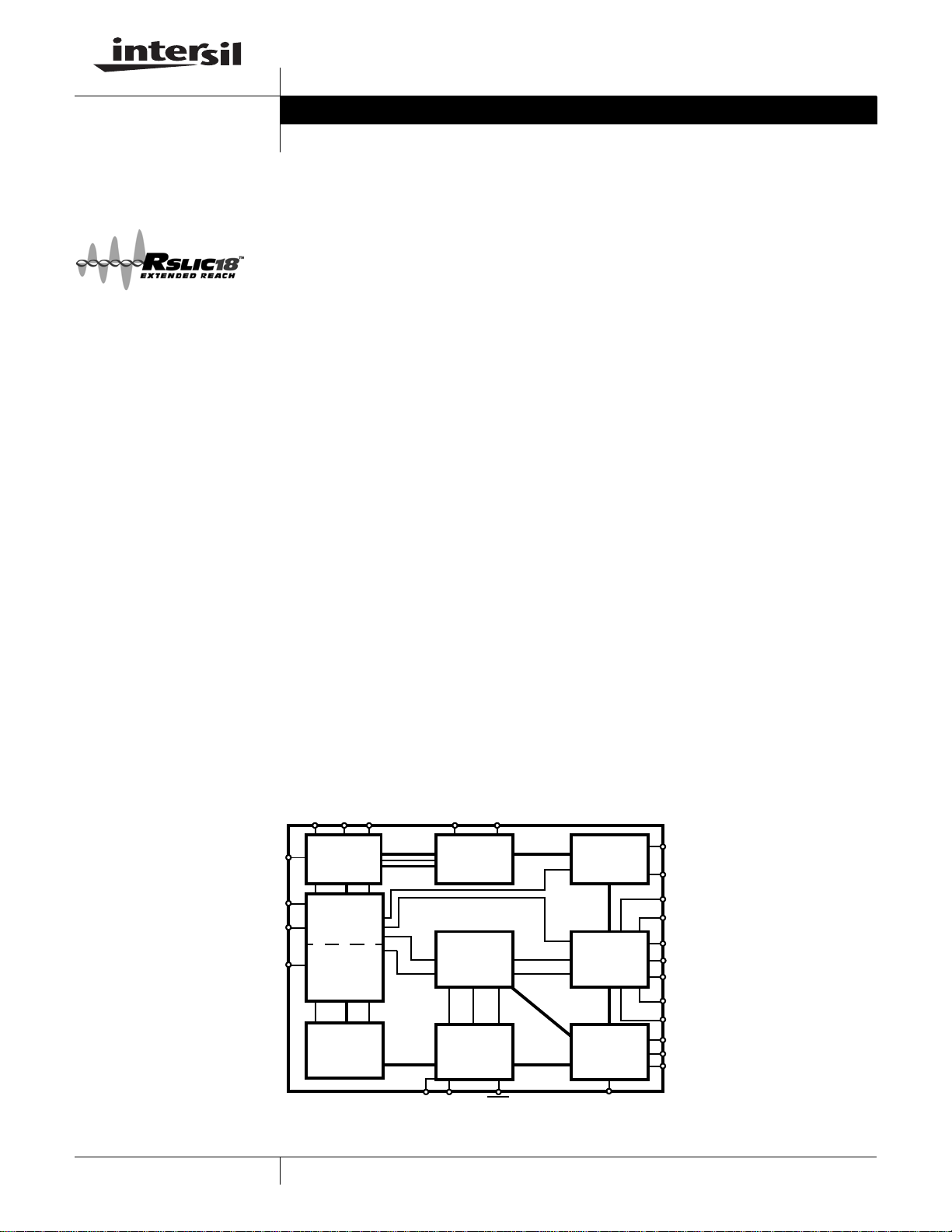
Block Diagram
V
TRANSMIT
DETECTOR
RTD DET
RD
CAUTION: These devices are sensitive to electrostatic discharge; follow proper IC Handling Procedures.
1-888-INTERSIL or 321-724-7143
BL
BATTERY
SWITCH
SENSING
LOGIC
BH
CONTROL
| Intersil (and design) is a registered trademark of Intersil Americas Inc.
Copyright Intersil Americas Inc. 2000, 2001, 2004. All Rights Reserved
ILIM
TIP
RING
TL
1
CDCP
POL CDCM V
DC
CONTROL
2-WIRE
PORT
TRANSIENT
CURRENT
LIMIT
INTERNAL
LOOP BACK
RSLIC18™ is a trademark of Intersil Corporation. All other trademarks mentioned are the property of their respective owners.
RINGING
PORT
4-WIRE
PORT
LOGIC
BSEL
V
V
V
V
-IN
V
V
V
V
F2
F1
F0
RSP
RSM
RXP
RXM
ZO
FB
TXP
TXM
ISL5586
www.BDTIC.com/Intersil
Ordering Information
HIGH BATTERY (V
BH
PART NUMBER
ISL5586FCM
ISL5586FCMZ (Note)
ISL5586FCMZ-T (Note)
ISL5586BIM
ISL5586BIMZ (Note)
ISL5586CIM
ISL5586CIMZ (Note)
ISL5586DIM
ISL5586DIMZ (Note)
••
••
••
••
••
••
NOTE: Intersil Pb-free products employ special Pb-free material sets; molding compounds/die attach materials and 100% matte tin plate termination
finish, which are RoHS compliant and compatible with both SnPb and Pb-free soldering operations. Intersil Pb-free products are MSL classified at
Pb-free peak reflow temperatures that meet or exceed the Pb-free requirements of IPC/JEDEC J STD-020C.
LONGITUDINAL
)
BALANCE
TEMP.
RANGE (°C) PACKAGE
••
••
••
0 to 75 28 Ld PLCC N28.45
0 to 75 28 Ld PLCC (Pb-free) N28.45
0 to 75 28 Ld PLCC Tape and Reel (Pb-free) N28.45
-40 to 85 28 Ld PLCC N28.45
-40 to 85 28 Ld PLCC (Pb-free) N28.45
-40 to 85 28 Ld PLCC N28.45
-40 to 85 28 Ld PLCC (Pb-free) N28.45
-40 to 85 28 Ld PLCC N28.45
-40 to 85 28 Ld PLCC (Pb-free) N28.45
PKG.
DWG. #100V 85V 75V 58dB 53dB
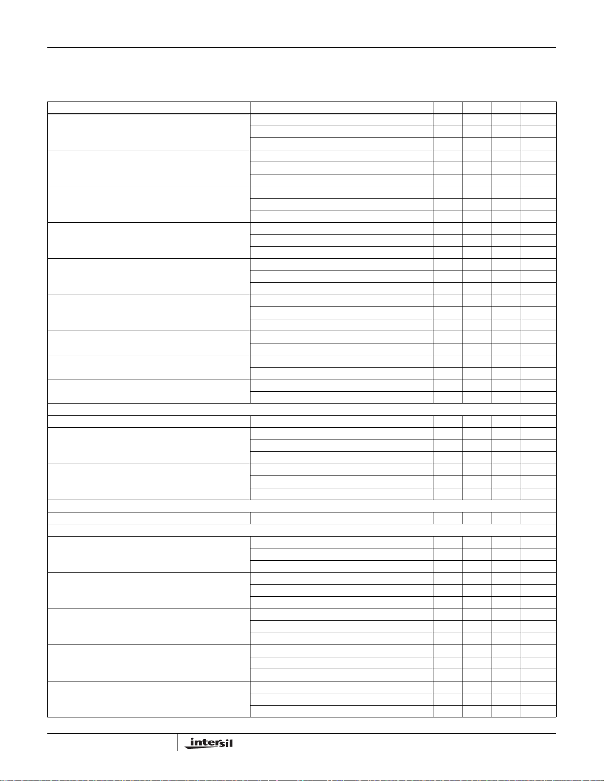
Device Operating Modes
MODE F2 F1 F0 DET DESCRIPTION
Low Power Standby (LPS) 0 0 0 SHD MTU compliant on hook operating mode.
Forward Active (FA) 0 0 1 SHD MTU compliant and OHT capable on hook mode, off hook loop feed mode.
Unused 0 1 0 n/a Reserved for internal purposes.
Reverse Active (RA) 0 1 1 SHD Signalling mode which reverses direction of loop current, otherwise like Forward Active.
Ringing 1 0 0 RTD Signalling mode used to generate high voltage balanced ringing signal.
Forward Loop Back (FLB) 1 0 1 SHD Internal loop back mode which connects internal load across Tip and Ring terminals.
Tip Open/Ground Start (TO) 1 1 0 SHD Signalling mode sets Tip to high impedance state, Ring output still active.
Power Denial (PD) 1 1 1 n/a Loop disconnect mode which forces both Tip and Ring to high impedance.
Pinout
ISL5586 (PLCC)
TOP VIEW
BSEL
F2
F1
F0
DET
V
RSP
V
RSM
BH
BGND
VBLV
4
3
5
6
7
8
9
10
11
12
13
14
TXP
TXM
V
V
AGND
RING
TIP
28
12
15
16
RXP
POL
V
LIM
I
RD
27
26
RTD
25
CDCM
24
CDCP
23
22
V
CC
TL
21
V
20
FB
-IN
19
17
18
ZO
V
RXM
V
2
FN4924.2
November 3, 2004
ISL5586
www.BDTIC.com/Intersil
Absolute Maximum Ratings T
Maximum Supply Voltages
V
. . . . . . . . . . . . . . . . . . . . . . . . . . . . . . . . . . . . . -0.5V to +7V
CC
- V
V
CC
ESD (Human Body Model) . . . . . . . . . . . . . . . . . . . . . . . . . . 500V
Maximum Tip/Ring Negative Voltage Pulse (Note 7) . . . . . .V
Maximum Tip/Ring Positive Voltage Pulse (Note 7). . . . . . . . . . + 8V
. . . . . . . . . . . . . . . . . . . . . . . . . . . . . . . . . . . . . . 110V
BAT
Operating Conditions
Temperature Range
Industrial. . . . . . . . . . . . . . . . . . . . . . . . . . . . . . . . . -40
Positive Power Supply (V
Negative Power Supply (V
CAUTION: Stresses above those listed in “Absolute Maximum Ratings” may cause permanent damage to the device. This is a stress only rating and operation of the
device at these or any other conditions above those indicated in the operational sections of this specification is not implied.
NOTE:
is measured with the component mounted on a low effective thermal conductivity test board in free air. See Tech Brief TB379 for details.
1. θ
JA
). . . . . . . . . . . . . . . . . . . . . . . . . . . .+5V
CC
, VBL). . . . . . . . . . . . . . -100V to -24V
BH
Electrical Specifications Unless Otherwise Specified, T
PARAMETER TEST CONDITIONS MIN TYP MAX UNITS
RINGING PARAMETERS
Input Impedance (Note 2) 35 - - MΩ
V
RSP
input impedance (Note 2) 10 - - MΩ
V
RSM
Differential Ringing Gain (Note 3) V
Ringing voltage Total Distortion R
4-Wire to 2-Wire Ringing Off Isolation Forward Active Mode, Referenced to V
2-Wire to 4-Wire Transmit Isolation Ringing Mode Referenced to the Differential
Centering Voltage Accuracy Tip, Referenced to V
AC TRANSMISSION PARAMETERS
Receive Input Impedance, V
Receive input Impedance, V
Transmit Output Impedance (Note 2) DC - 0.01 - Ω
Transmit Output Drive Capability (Note 2) Current 0.30 1.0 - mA
4-Wire Port Overload Level THD = 1% 3.1 3.5 - V
2-Wire Port Overload Level THD = 1% 3.1 3.5 - V
2-Wire Return Loss (Note 2) 200Hz ≤ f ≤ 1kHz - 35 - dB
Longitudinal Current Capability per Wire (Note 2) False Detect 20 - - mA
2-Wire Longitudinal Balance (ON-Hook and OFF-Hook)
(Notes 4, 5)
4-Wire Longitudinal Balance (ON-Hook and OFF-Hook)
(Notes 4, 5)
4-Wire to 2-Wire Insertion Loss 0dBmo at 1kHz 2.72 2.92 3.12 dB
2-Wire to 4-Wire Insertion Loss 0dBmo at 1kHz -0.2 0 0.2 dB
4-Wire to 4-Wire Insertion Loss 0dBmo at 1kHz 2.72 2.92 3.12 dB
Frequency Response, On Hook, 2-Wire to 4-Wire, 4-Wire
to 2-Wire, 4-Wire to 4-Wire
Frequency Response, Off Hook
2-Wire to 4-Wire, 4-Wire to 2-Wire, 4-Wire to 4-Wire
RXP
RXM
= 25oC Thermal Information
A
BH
-15V
Thermal Resistance (Typical, Note 1) θ
PLCC Package. . . . . . . . . . . . . . . . . . . . . . . . . . . . . 53
Maximum Junction Temperature Plastic . . . . . . . . . . . . . . . . . 150
Maximum Storage Temperature Range. . . . . . . . . . -65
Maximum Lead Temperature (Soldering 10s) . . . . . . . . . . . . . 300
(PLCC - Lead Tips Only)
(oC/W)
JA
o
C to 150oC
Die Characteristics
o
C to 85oC
= -40oC to 85oC, VBL = -24V, VBH = -100V, VCC = +5V, AGND = BGND = 0V,
loop current limit = 25mA. All AC Parameters are specified at 600
frequency band of 300Hz to 3.4kHz. Protection resistors = 0
product offering.
(Note 2) 379 541 - kΩ
(Note 2) 100 142 - kΩ
A
to 2-Wire, R
RS
= 1.3 kΩ, V
L
Ringing Amplitude.
Ring, Referenced to V
Capacitance to Ground - 1.0 100 pF
1kHz ≤ f ≤ 3.4kHz - 23 - dB
False Detect in Low Power Standby 10 - - mA
200Hz, 500Hz, 1000Hz 58 61 - dB
3000Hz 53 61 - dB
200Hz, 500Hz, 1000Hz 58 64 - dB
3000Hz 53 62 - dB
Referenced to 0dBmo at 1004Hz,
400Hz ≤ f ≤ 2800Hz
Referenced to 0dBmo at 1004Hz, f = 400Hz,
2800Hz
Substrate Potential . . . . . . . . . . . . . . . . . . . . . . . . . . . . . . . . . -V
Process . . . . . . . . . . . . . . . . . . . . . . . . . . . . . . . . . . . . . . Bipolar-DI
Ω, 2-wire terminating impedance over the
Ω. These parameters apply generically to each
= 5 REN - 99.5 - V/V
LOAD
= |VBH| -5 - 0.8 5 %
T-R
Input. - 100 - dB
RS
- 100 - dB
/2 + 0.5V -3.0 0.2 3.0 V
BH
+ 0.5V -3.0 0.2 3.0 V
BH/2
-0.15 0.03 0.15 dB
-0.15 0.03 .15 dB
PEAK
PEAK
o
o
BH
RMS
RMS
C
C
3
FN4924.2
November 3, 2004
ISL5586
www.BDTIC.com/Intersil
Electrical Specifications Unless Otherwise Specified, T
loop current limit = 25mA. All AC Parameters are specified at 600
frequency band of 300Hz to 3.4kHz. Protection resistors = 0
product offering. (Continued)
PARAMETER TEST CONDITIONS MIN TYP MAX UNITS
Amplitude Tracking, Off Hook, 2-Wire to 4-Wire, 4-Wire to
2-Wire, 4-Wire to 4-Wire
Amplitude Tracking, ON-Hook 0dBmo to -37dBmo, f = 1004Hz,
Signal to Distortion, 2-Wire to 4-Wire, 4-Wire to 2-Wire,
4-Wire to 4-Wire, ON-Hook and OFF-Hook
Signal Frequency Distortion (0Hz to 12kHz) 0dBmo input, 0 Hz ≤ f ≤ 12kHz 28 45 - dB
Single Frequency Distortion (0Hz to 4kHz) 0dBmo Input, 1004Hz ≤ f ≤ 1024Hz 40 50 - dB
Intermodulation Distortion, 2-Wire to 4-Wire,
4-Wire to 2-Wire, 4-Wire to 4-Wire
(IEEE Standard 743-1984)
Idle Channel Noise, 2-Wire (Note 5) C-Message, Forward Active, Low Battery Enabled - 10.0 13.0 dBrnc
Idle Channel Noise, 4-Wire (Note 5) C-Message, Forward Active, Low Battery Enabled - 10.0 13.0 dBrnc
DC PARAMETERS
OFF-Hook Loop Current Limit Programming Accuracy (1% External Resistor) -8.5 1.0 +8.5 %
OFF-Hook Transient Current Limit Programming Accuracy -10 - +10 %
Loop Current During Low Power Standby Forward Polarity Only (R
Open Circuit Voltage
(|Tip - Ring|)
Forward and Reverse Active modes
Open Circuit Voltage (|Tip-Ring|) LPS VBH > -60V 43 51 - V
Absolute Open Circuit Voltage (Relative to GND) V
Absolute Open Circuit Voltage V
TEST ACCESS FUNCTIONS
Loopback Max Battery --52V
LOOP DETECTORS AND SUPERVISORY FUNCTIONS
Switch Hook Programming Range 5-15mA
Switch Hook Programming Accuracy Assumes 1% External Programming Resistor -10 - +10 %
Dial Pulse Distortion -1.0- %
Ring Trip Comparator Threshold 2.32.602.9 V
Ring Trip Programming Current Accuracy -10 - +10 %
Thermal Shutdown Threshold IC Junction Temperature - 175 -
LOGIC INPUTS (F0, F1, F2, BSEL)
Input Low Voltage --0.8V
Input High Voltage 2.0 - - V
Input Low Current (F0, F1, F2) V
Input Low Current (BSEL) V
Input High Current (F0, F1, F2, BSEL) V
LOGIC OUTPUT (DET
Output Low Voltage I
Output High Voltage I
SUPPLY CURRENTS
Low Power Standby, BSEL = 2.0V, V
Forward or Reverse, BSEL =.8V I
)
= -75V to -100V I
BH
= -40oC to 85oC, VBL = -24V, VBH = -100V, VCC = +5V, AGND = BGND = 0V,
A
Ω, 2-wire terminating impedance over the
Ω. These parameters apply generically to each
+3dBmo to -37dBmo, f = 1004Hz,
Referenced to 0dBmo
-37 to -50dBmo - 0.05 - dB
-50 to -55dBmo - 0.10 - dB
Referenced to 0dBmo
Input level 0dBmo to -30dBmo 33 45 - dB
Input Level -30 to -40dBmo 27 40 - dB
Input Level -40 to -45dBmo 22 29 - dB
4-Tone Second-Order Intermodulation Products 43 50 - dB
4-Tone Third-order Intermodulation Products 44 62 - dB
Programming Range 15 - 45 mA
Programming Range 40 - 100 mA
= 600Ω) -24- mA
L
V
= -16V - 7.0 - V
BL
VBL = -24V 13.5 14.5 16.5 V
VBH > -60V 43 48 - V
in FA, V
RG
in LPS - -52 -56 V
RG
= 0.4V - 7.5 20 µA
IL
= 0.4V - 1.0 - µA
IL
= 2.4V - 0.01 - µA
IH
= 5mA - 0.15 0.4 V
OL
= 100µA 2.4 3.2 3.5 V
OH
CC
I
BH
CC
I
BL
in RA, VBH > -60V - -53 -56 V
TG
-0.02- dB
-0.01- dB
DC
DC
DC
DC
DC
DC
o
-3.25.0mA
- 0.65 0.9 mA
-5.06.5mA
-1.52.5mA
C
4
FN4924.2
November 3, 2004
ISL5586
www.BDTIC.com/Intersil
Electrical Specifications Unless Otherwise Specified, T
loop current limit = 25mA. All AC Parameters are specified at 600
frequency band of 300Hz to 3.4kHz. Protection resistors = 0
= -40oC to 85oC, VBL = -24V, VBH = -100V, VCC = +5V, AGND = BGND = 0V,
A
Ω, 2-wire terminating impedance over the
Ω. These parameters apply generically to each
product offering. (Continued)
PARAMETER TEST CONDITIONS MIN TYP MAX UNITS
Forward Active, BSEL = 2.0V, VBH = -100V I
Forward Active, BSEL = 2.0V, V
Forward Active, BSEL = 2.0V, V
Ringing, BSEL = 2.0V, V
Ringing, BSEL = 2.0V, V
Ringing, BSEL = 2.0V, V
BH
BH
BH
Forward Loopback, BSEL = 0.8V, V
= -85V I
BH
= -75V I
BH
= -100V I
= -85V I
= -75V I
= -24V I
BL
Tip Open, BSEL = 2.0V I
Power Denial, BSEL = 0.8V or 2.0V I
CC
I
BL
I
BH
CC
I
BL
I
BH
CC
I
BL
I
BH
CC
I
BL
I
BH
CC
I
BL
I
BH
CC
I
BL
I
BH
CC
I
BL
CC
I
BL
CC
I
BL
-7.09.0mA
-1.42.0mA
-1.83.0mA
-6.68.5mA
- 1.35 2.0 mA
- 1.60 2.75 mA
-6.38.0mA
- 1.25 2.0 mA
- 1.45 2.5 mA
- 7.4 10.0 mA
-1.52.0mA
-2.23.0mA
- 6.80 9.25 mA
- 1.36 2.0 mA
-2.13.0mA
-6.48.5mA
- 1.26 2.0 mA
-2.03.0mA
- 10.3 13.5 mA
- 23.0 32.0 mA
-3.2- mA
-0.1- mA
-3.46.0mA
- 0.22 0.50 mA
ON HOOK POWER DISSIPATION (Note 6)
Forward or Reverse V
Low Power Standby V
Ringing V
= -24V - 57 - mW
BL
= -100V - 83 - mW
BH
= -85V - 70 - mW
V
BH
V
= -75V - 64 - mW
BH
= -100V - 294 - mW
BH
= -85V - 236 - mW
V
BH
= -75V - 206 - mW
V
BH
OFF HOOK POWER DISSIPATION (Note 6)
Forward or Reverse V
= -24V, I
BL
= 25mA, RL = 300Ω - 305 - mW
LIM
POWER SUPPLY REJECTION RATIO
V
to 2-Wire, BSEL = 0.8V f = 50kHz - 50 - dB
CC
f = 300Hz ≤ f ≤ 3400Hz - 45 - dB
f = 8kHz ≤ f ≤ 16kHz - 28 - dB
to 4-Wire, BSEL = 0.8V f = 50Hz - 70 - dB
V
CC
f = 300Hz ≤ f ≤ 3400Hz - 55 - dB
f = 8kHz ≤ f ≤ 16kHz - 40 - dB
V
to 2-Wire, BSEL = 0.8V f = 50Hz - 25 - dB
BL
f = 300Hz ≤ f ≤ 3400Hz - 38 - dB
f = 8kHz ≤ f ≤ 16kHz - 28 - dB
to 4-Wire, BSEL = 0.8V f = 50Hz - 27 - dB
V
BL
f = 300Hz ≤ f ≤ 3400Hz - 36 - dB
f = 8kHz ≤ f ≤ 16kHz - 23 - dB
V
to 2-Wire, BSEL = 2.0V f = 50Hz - 27 - dB
BH
f = 300Hz ≤ f ≤ 3400Hz - 35 - dB
f = 8kHz ≤ f ≤ 16kHz - 23 - dB
5
FN4924.2
November 3, 2004
ISL5586
www.BDTIC.com/Intersil
Electrical Specifications Unless Otherwise Specified, T
loop current limit = 25mA. All AC Parameters are specified at 600
frequency band of 300Hz to 3.4kHz. Protection resistors = 0
product offering. (Continued)
PARAMETER TEST CONDITIONS MIN TYP MAX UNITS
VBH to 4-Wire, BSEL = 2.0V f = 50Hz - 76 - dB
NOTES:
2. These parameters are controlled via design and Statistical Process Control and are not directly tested. These parameters are characterized upon
initial design release and upon design changes which would affect these characteristics.
3. Input voltage = 0.636V
4. Tested per IEEE455-1985, with 368Ω resistors connected to the Tip and Ring terminals.
5. These parameters are tested 100% at room temperature, and are guaranteed but not tested across the full temperature range via statistical
characterization and design.
6. The power dissipation is based on actual device measurements and will be less than worst case calculations based on data sheet supply current limits.
7. Characterized with 2 x 10us and 10 x 1000us first level lightning surge waveform (GR-1089-CORE).
for VBH = -100V, 0.530V
RMS
RMS
= -40oC to 85oC, VBL = -24V, VBH = -100V, VCC = +5V, AGND = BGND = 0V,
A
Ω, 2-wire terminating impedance over the
Ω. These parameters apply generically to each
f = 300Hz ≤ f ≤ 3400Hz - 55 - dB
f = 8kHz ≤ f ≤ 16kHz - 42 - dB
for VBH = -85V and 0.460V
for -75V devices.
RMS
Design Equations
Refer to Figure 14 for programming resistor connections.
Loop Supervision Thresholds
SWITCH HOOK DETECT
The desired switch hook detect threshold current (I
a single external resistor, R
R
615 ISH⁄=
SH
as follows
SH
) is set by
SH
(EQ. 1)
The loop current threshold programming range is from 5mA
to 15mA.
RING TRIP DETECT
The ring trip detect threshold (I
resistor, R
R
RT
should be set between the peak ringing current and the
I
RT
RT
1800 IRT⁄=
as follows.
) is set by a single external
RT
(EQ. 2)
peak off hook current while still ringing. In addition, the ring
trip current must be set below the transient current limit
including tolerances. The ringing signal filter capacitor C
in parallel with R
sets the ring trip response time.
RT
RT
LOOP CURRENT LIMIT
The DC loop current limit (I
external resistor R
1760
------------ -=
R
IL
I
LIM
as follows.
IL
) is programmed by the
LIM
(EQ. 3)
The loop current limit programming range is from 15mA to
45mA.
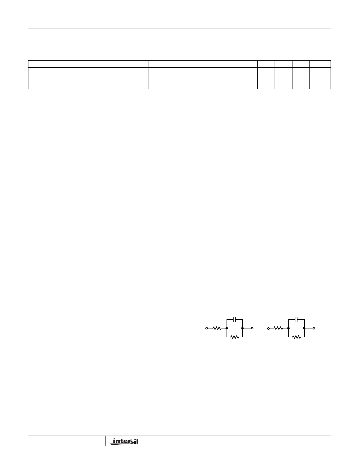
Impedance Matching
The AC source impedance of the SLIC is programmed with
the external impedance network Z
synthesize and match Resistive line terminations the
programming network is simply a resistor (R
as described next. To
S
) as shown in
S
,
Figure 14. For complex line terminations such as the one
illustrated in Figure 1, a complex programming network is
required.
RESISTIVE IMPEDANCE SYNTHESIS
The AC source resistance of the SLIC is synthesized with a
single external resistor R
400
R
SZ0
--------- -
× 133.3 Z
3
The synthesized resistance (Z
as follows:
S
()==
0
) is determined by the
0
(EQ. 4)
characteristic line resistance and protection resistors as
shown in Equation 5.
Z
ORL
RP1RP2+()–=
(EQ. 5)
COMPLEX IMPEDANCE SYNTHESIS
A complex network is used in place of RS when the termination
impedance of the line is complex as shown in Figure 1.
2-WIRE TERMINATION
IMPEDANCE (ZL)
C
2
R
1
R
2
FIGURE 1. COMPLEX PROGRAMMING NETWORK
The component R
R
used for resistive impedance synthesis. The design
S
has a different design equation than the
S
PROGRAMMING
NETWORK (ZS)
C
P
R
S
R
P
equations for each component are provided below where
RP1 and RP2 are the protection resistors and R
P
is a
component of the programming network.
RS133.3 R1 RP1– RP2–()×=
R
P
133.3 R2×=
(EQ. 6)
(EQ. 7)
6
FN4924.2
November 3, 2004

ISL5586
www.BDTIC.com/Intersil
CPC2133.3⁄=
Z
O
R1 RP1– RP2–()R2 C2+=
(EQ. 8)
(EQ. 9)
4-WIRE TO 2-WIRE GAIN
The 4-wire to 2-wire gain (G
) is defined as the receive
42
gain. It is a function of the terminating impedance,
synthesized impedance and protection resistors. The gain is
defined from the Receive input terminals (V
the terminating impedance (Z
) on the 2-wire side, and is
L
RXP
, V
RXM
) to
illustrated in Figure 12.
Z
G
2.8
–=
42
L
------------------------------------------
ZO + 2 RP + Z
L
(EQ. 10)
When the device source impedance and the protection
resistors equal the terminating impedance, the receive gain
equals 2.92dB and is inverted with respect to the input.
2-WIRE TO 4-WIRE GAIN
The 2-wire to 4-wire gain (G
) is the gain from tip and ring to
24
the transmit differential output. The transmit gain is given by
Equation 11. Note that V
protection resistors (reference Figure 13). With Z
is defined on the line side of the
TR
set to 600
L
ohms, the protection resistors set to 50Ω/terminal and
Z
-2RP the Transmit gain equals -0.833 (-1.59dB) and
0=ZL
is inverted with respect to the 2-wire input (V
Z
G
2
–=
24
O
------------------------------------------
ZO + 2 RP + Z
L
TR
).
(EQ. 11)
TRANSHYBRID GAIN
The transhybrid gain is defined as the 4-wire to 4-wire gain
) and is given by Equation 12 (Reference Figure 14)).
(G
44
Z
–=
G
2.8
44
O
---------------------------------------
ZO2RPZ
++
L
(EQ. 12)
Transient Current Limit
The drive current capability of the output amplifiers is
determined by an externally programmable output current
limit circuit which is separate from the DC loop current limit
function. The transient current limit is programmed with a
resistor to ground at the TL pin. The current limit circuit
works in both the source and sink direction, with an internally
fixed offset to prevent the current limit functions from turning
on simultaneously. The current limit function is provided by
sensing line current and reducing the voltage drive to the
load when the externally set threshold is exceeded, hence
forcing a constant source or sink current.
SOURCE CURRENT PROGRAMMING
The source current is externally programmed as shown in
Equation 13.
1780
R
-------------=
TL
I
SRC
(EQ. 13)
For example, a source current limit setting of 50mA is
programmed with a 35.6kΩ resistor connected from pin 16 of
the device to ground. This setting determines the maximum
amount of current which flows from Tip to Ring during an off
hook event until the DC loop current limit responds. In addition
this setting also determines the amount of current which will
flow from Tip or Ring when external battery faults occur.
SINK CURRENT PROGRAMMING
The sink current limit is internally offset 20% higher than the
externally programmed source current limit setting.
I
SNK
1.20 I
×=
SRC
(EQ. 14)
If the source current limit is set to 50mA, the sink current limit
will be 60mA. This setting will determine the amount of current
which flows into Tip or Ring when external ground faults occur.
FUNCTIONAL DESCRIPTION
Each amplifier is designed to limit source current and sink
current. The diagram below shows the functionality of the
circuit for the case of limiting the source current. A similar
diagram applies to the sink current limit with current polarity
changed accordingly.
IO/K
I
= 1.21/TL
REF
I
SIG
FIGURE 2. CURRENT LIMIT FUNCTIONAL DIAGRAM
During normal operation, the error current (I
the output voltage is determined by the signal current (I
VB/2
I
ERR
+
200K
20
TIP or RING
) is zero and
ERR
I
O
SIG
multiplied by the 200K feedback resistor. With the current
polarity as shown for I
, the output voltage moves positive
SIG
with respect to half battery. Assuming the amplifier output is
driving a load at a more negative potential, the amplifier
output will source current.
During excessive output source current flow, the scaled
output current (I
forcing an error current (I
/K) exceeds the reference current (I
O
). With the polarity as shown
ERR
REF
)
the error current subtracts from the signal current, which
reduces the amplifier output voltage. By reducing the output
voltage the source current to the load is decreased and the
output current is limited.
DETERMINING THE PROPER SETTING
Since this feature programs the maximum output current of
the device, the setting must be high enough to allow for
detection of ring trip or programmed off hook loop current,
whichever is greater.
)
7
FN4924.2
November 3, 2004

ISL5586
www.BDTIC.com/Intersil
To allow for proper ring trip operation, the transient current
limit setting should be set at least 25% higher than the peak
ring trip current setting. Setting the transient current 25%
higher should account for programming tolerances of both
the ring trip threshold and the transient current limit.
If loop current is larger than ring trip current (low REN
applications) then the transient current limit should be set at
least 35% higher than the loop current setting. The slightly
higher offset accounts for the slope of the loop current limit
function.
Attention to detail should be exercised when programming
the transient current limit setting. If ring trip detect does not
occur while ringing, then re-examine the transient current
limit and ring trip threshold settings.
Low Power Standby Mode
Overview
The low power standby mode (LPS, 000) should be used in
conjunction with the high battery during idle line conditions.
The SLIC is designed to operate from the high battery during
this mode so MTU compliance can be met. Most of the
internal circuitry is powered down, resulting in low power
dissipation. If MTU compliance is not required during idle line
conditions, the device may be operated from the low battery
which will decrease the standby power dissipation.
TABLE 1. DEVICE INTERFACES DURING LPS
INTERFACE ON OFF NOTES
Receive - x AC transmission, impedance
Ringing - x
Transmit - x
2-Wire x - Amplifiers disabled.
Loop Detect x - Switch hook.
2-Wire Interface
In the LPS mode, the 2-wire interface is maintained with
internal switches, resistors, and voltage references. The Tip
and Ring amplifiers are turned off to conserve power. The
device will provide MTU compliance, loop current, and loop
supervision. Figure 2 represents the internal circuitry
providing the 2-wire interface when in this mode of operation.
matching and ringing are
disabled during this mode.
GND
600Ω
TIP AMP
TIP
RING
RING AMP
600Ω
MTU REF
FIGURE 3. LPS 2-WIRE INTERFACE CIRCUIT DIAGRAM
MTU Compliance
Maintenance Termination Unit or MTU compliance places
DC voltage requirements on the 2-wire terminals during idle
line conditions. The minimum idle voltage for compliance is
42.75V. The high side of the MTU range is 56V. The voltage
is expressed as the difference between Tip and Ring.
The Tip voltage is held near ground through a 600Ω resistor
and switch. The Ring voltage is nominally limited to -49V by
the MTU reference. A switch and 600Ω resistor connect the
MTU reference to the Ring terminal. When the high battery
voltage exceeds the MTU reference of -49V, the Ring
terminal will be clamped by the internal reference. The same
Ring relationships apply when operating from the low
battery. For operating battery voltages (V
) less than or
BH
equal to the internal MTU reference, the Ring voltage will be
approximately 4.5 volts more positive than V
BH
.
Loop Current
In the LPS mode, the device is capable of providing DC
current to a load through a path of resistors and switches.
The current available for switch hook detect is a function of
the off hook loop resistance (R
hook phone resistance and copper loop resistance. The
current available during LPS is given by Equation 15.
I
LOOP
1– 49–()–()600 600 R
++()⁄=
Internal current limiting of the standby switches will limit the
maximum current to approximately 23mA. The longitudinal
current capability is guaranteed to be greater than or equal to
10mA
per pin. When longitudinal currents exceed this
RMS
level, false off hook detection may occur. The reduction in
longitudinal current capability with respect to the Forward Active
mode is a result of turning off the Tip and Ring amplifiers.
). This includes the off
LOOP
LOOP
(EQ. 15)
On Hook Power Dissipation
The on hook power dissipation of the SLIC in the LPS mode
is determined by the operating voltages and quiescent
currents and is calculated below.
P
LPSVBHIBHQ
× VBLI
8
× VCCI
BLQ
×++=
CCQ
(EQ. 16)
FN4924.2
November 3, 2004

ISL5586
www.BDTIC.com/Intersil
The quiescent current terms are specified in the electrical
tables for each operating mode. Load power dissipation is
not a factor since this is an on hook mode. Some
applications may specify a standby current. The standby
current may be a charging current required for modern
telephone electronics.
Standby Current Power Dissipation
Any standby line current, I
dissipation term P
. Equation 17 illustrates the power
SLC
contribution is zero when the standby line current is zero.
P
SLCISLCVBH
If the battery voltage is less than -49V (the MTU clamp is
off), the standby line current power contribution reduces to
Equation 18.
P
SLCISLCVBH
Most applications do not specify charging current
requirements during standby. When specified, the typical
charging current may be as high as 5mA.
, introduces an additional power
SLC
49– 1I
1I
SLC
SLC
x1200++()×=
x1200++()×=
(EQ. 17)
(EQ. 18)
Forward Active Mode
Overview
The Forward Active mode (FA, 001) is the primary AC
transmission mode of the SLIC. On hook transmission, DC loop
feed and voice transmission are supported during this mode.
The device may be operated from either high or low battery for
on-hook transmission and from low battery for loop feed.
Loop supervision is provided by the switch hook detector at
the DET
be selected for DC loop feed and voice transmission.
On-Hook Transmission
The primary purpose of on hook transmission will be to
support caller ID and other advanced signalling features.
The transmission over load level while on hook is 3.1V
When operating from the high battery, the DC voltages at Tip
and Ring are MTU compliant. The typical Tip voltage is -4V
and the Ring voltage is a function of the battery voltage for
battery voltages less than -60V as shown in Equation 19.
V
output. When DET goes low, the low battery should
RINGVBH
4.5V+=
PEAK
(EQ. 19)
R
B
R
V
OUT
R
L
FIGURE 4. VOLTAGE FEED CURRENT SENSE DIAGRAM
CS
-
+
-
+
K
S
R
A
V
IN
R
C
By monitoring the current at the amplifier outputs, a negative
feedback mechanism sets the output voltage for a defined
load. The amplifier closed loop gains are set by internal
resistor ratios (R
, RB, RC) providing all the performance
A
benefits of matched resistors. The internal sense resistor
R
, is much smaller than the gain resistors and are
CS
typically 20Ω. The feedback mechanism, K
, represents the
S
gain configuration providing negative feedback to the loop.
DC Loop Feed
The feedback mechanism for monitoring the DC portion of
the loop current is contained within the loop detector block. A
low pass filter is used in the feedback loop to block voice and
other signals from interfering with the loop current limit
function. The pole of the low pass filter is set by the external
4.7µF capacitor (C
feed characteristic of the SLIC will drive Tip and Ring
towards half battery to regulate the DC loop current. For light
loads, Tip will be near -4V and Ring will be near
V
+ 4.5V. Most applications will operate the device from
VBL
low battery while off hook. The following diagram depicts the
DC feed characteristic.
V
TR(OC)
, DC (V)
.
TR
V
FIGURE 5. DC FEED CHARACTERISTIC
The point on the y-axis labeled V
Tip to Ring voltage and is defined by the feed battery
voltage.
and an internal 8KΩ resistor. The DC
DC)
m = (∆VTR/∆IL) = 11.1kΩ
I
I
LOOP
(mA)
LIM
TR(OC)
is the open circuit
Feed Architecture
The SLIC design implements a voltage feed current sense
architecture. The voltage across Tip and Ring is controlled
by sensing the load current. Resistors are placed in series
with the Tip and Ring outputs to provide the current sensing
function. The diagram below illustrates the concept.
V
TR OC()VBL
The curve of Figure 5 shows the loop current for a given set
of loop conditions. The loop conditions are determined by
the low battery voltage and the DC loop resistance. The DC
loop resistance is the sum of the protection resistance,
copper resistance (ohms/foot) and the telephone off hook
DC resistance.
9
9–=
(EQ. 20)
FN4924.2
November 3, 2004

ISL5586
www.BDTIC.com/Intersil
I
A
I
B
R
(Ω)
KNEE
LOAD CHARACTERISTIC
FIGURE 6. I
I
SC
I
LIM
(mA)
LOOP
I
LOOP
2R
P
R
LOOP
VERSUS R
LOOP
The slope of the feed characteristic and the battery voltage
define the maximum loop current on the shortest possible
loop as the short circuit current I
I
SCILIM
The term I
line segment I
V
------------------------------------------------------+=
is the programmed current limit, 1760/RIL. The
LIM
A
–
TR OC()2RPILIM
1.1e 4
represents the constant current region of the
SC
.
(EQ. 21)
loop current limit function.
I
AILIM
V
--------------------------------------------------------------+=
–
TR OC()RLOOPILIM
1.1e 4
(EQ. 22)
The maximum loop resistance for a programmed loop
current is defined as R
V
R
KNEE
When R
TR OC()
------------------------=
I
LIM
is exceeded, the device will transition from
KNEE
KNEE
.
(EQ. 23)
constant current feed to constant voltage, resistive feed. The
line segment I
represents the resistive feed portion of the
B
load characteristic.
V
I
B
TR OC()
------------------------=
R
LOOP
(EQ. 24)
Power Dissipation
The power dissipated by the SLIC in the Forward Active
mode while on hook is strictly a function of the quiescent
currents for each supply.
Since the current relationships are different for constant
current versus constant voltage, the region of device
operation is critical to valid power dissipation calculations.
Reverse Active Mode
Overview
The reverse active mode (RA, 011) provides the same
functionality as the forward active mode. On hook transmission,
DC loop feed, and voice transmission are supported. Loop
supervision is provided by the switch hook detector. The device
may be operated from either high or low battery.
When in the Reverse Active mode the Tip and Ring DC
voltage characteristics exchange roles. That is, Ring is
typically 4V below ground and Tip is typically 4.5V more
positive than battery.
Silent Polarity Reversal
Changing from forward active to reverse active or vice versa
is referred to as polarity reversal. Many applications require
control of the polarity reversal transition time. Requirements
range from minimizing cross talk to protocol signalling.
The SLIC uses an external low voltage capacitor, C
set the reversal time. The capacitor is isolated from the AC
loop so that loop stability is not influenced by its selection.
Once C
is set, the reversal time will remain nearly
POL
constant over various load conditions.
The internal circuitry used to set the polarity reversal time is
shown in Figure 7. During Forward Active the switch is open
and the current from source I1 charges the external timing
capacitor C
. The internal resistor provides a clamping
POL
function for the voltage at the POL node. When the Reverse
Active mode is initiated the switch closes and the difference
current (I2-I1) discharges the timing capacitor. The voltage at
the POL node drives one side of a transistor differential pair
which forces the Forward or Reverse condition on the Tip and
Ring amplifiers. The forward/reverse transition time is given by
Equation 28, where ∆time is the required reversal time.
POL
, to
P
FAQVBH
I×
BHQ
VBLI
× V
BLQ
×++=
CCICCQ
(EQ. 25)
Off hook power dissipation is increased above the quiescent
power dissipation by the DC load. If the loop length is less
than or equal to R
current (I
, and the power dissipation is calculated using
A)
, the device is providing constant
KNEE
C
Polarized capacitors may be used for C
at the POL pin and minimal voltage excursion in the order of
±0.75V, are well suited for polarized capacitors.
POL
∆time
----------------=
75000
Equation 26.
P
FA IA()PFA Q()VBLxIA
()R
()–+=
If the loop length is greater than R
LOOP
KNEE
2
xI
A
, the device is
(EQ. 26)
operating in the constant voltage, resistive feed region. The
power dissipated in this region is calculated using Equation 27.
P
FA IB()PFA Q()VBLxIB
()R
()–+=
LOOP
2
xI
B
(EQ. 27)
10
. The low voltage
POL
November 3, 2004
(EQ. 28)
FN4924.2

I
www.BDTIC.com/Intersil
1
POL
75kΩ
I
2
FIGURE 7. REVERSAL TIMING CONTROL
C
POL
Power Dissipation
The power dissipation equations for forward active operation
also apply to the reverse active mode.
Ringing
Overview
The Ringing mode (RNG, 100) provides linear amplification
to support a variety of ringing waveforms. A programmable
ring trip function provides loop supervision and auto
disconnect upon ring trip. The device is designed to operate
from the high battery during this mode.
Architecture
The SLIC provides linear amplification to the differential
signal applied to the ringing inputs (V
differential ringing gain of the device is 100V/V. The circuit
model for the ringing path is shown in Figure 8.
R
20
-
TIP
RING
+
5:1
V
+
20
+
-
R
FIGURE 8. LINEAR RINGING MODEL
BH
-
2
RSP
R/8
1.25R
V
RSP
, V
+
-
RSM
). The
+
-
V
RSM
1.25R
RR
+
-
ISL5586
V
BH
-----------
V
R
2
×()–=
50 V
DIF
(EQ. 30)
When the differential input signal is zero, the Tip and Ring
amplifier outputs are centered at half battery. The device
provides auto centering for easy implementation of
sinusoidal ringing waveforms. Both AC and DC control of the
Tip and Ring outputs is available during ringing. This feature
allows for DC offsets as part of the ringing waveform.
Ringing Input Terminals
The differential terminals feature high input impedance
which allows the use of low value capacitors for AC coupling
the ring signal if necessary. The Ringing input is enabled
only during the ringing mode, therefore a free running
oscillator may be connected at all times.
When operating from a battery of -100V, each amplifier, Tip
and Ring, will swing a maximum of 95V
maximum differential signal swing between V
to achieve full scale ringing is approximately 1.9V
. Hence, the
P-P
RSP
and V
.
P-P
RSM
Logic Control
Ringing patterns consist of silent and ringing intervals. The
ringing to silent pattern is called the ringing cadence. During
the silent portion of ringing, the device can be programmed
to any other operating mode. The most likely candidates are
low power standby or forward active. Depending on system
requirements, the low or high battery may be selected.
Loop supervision is provided with the ring trip detector. The ring
trip detector senses the change in loop current when the phone
is taken off hook. The loop detector full-wave rectifies the
ringing current, which is then filtered with external components
R
and CRT. The resistor RRT sets the trip threshold and the
RT
capacitor C
require a trip response time less than 150ms.
Three very distinct actions occur when the device detects a
ring trip. First, the DET
mechanism eliminates the need for software filtering of the
detector output. The latch is cleared when the operating
mode is changed externally. Second, the Ringing inputs are
disabled, removing the ring signal from the line. Third, the
device is internally forced to the forward active mode.
sets the trip response time. Most applications will
RT
output is latched low. The latching
The voltage gain from the differential ringing input to the Tip
output is 50V/V. The resistor ratios provide a gain of 10 and
the current mirror provides a gain of 5. The voltage gain from
the differential input to the Ring output is -50V/V. The
equations for the Tip and Ring outputs during ringing are
provided below.
V
----------- 50 V
V
T
BH
2
×()+=
DIF
(EQ. 29)
11
The power dissipation during ringing is dictated mostly by the
load driving requirements and the ringing waveform. The key to
valid power calculations is the correct definition of average and
RMS currents. The average current defines the high battery
supply current. The RMS current defines the load current.
The cadence provides a time averaging reduction in the
peak power. The total power dissipation consists of ringing
power, P
P
, and the silent interval power, Ps.
r
--------------
RNGPr
× P
trts+
Power Dissipation
t
r
t
s
--------------
×+=
s
trts+
(EQ. 31)
FN4924.2
November 3, 2004

ISL5586
www.BDTIC.com/Intersil
The terms tR and tS represent the cadence. The ringing
interval is t
ratio t
and the silent interval is tS. A typical cadence
R
is 1:2.
R:tS
The quiescent power of the device in the Ringing mode is
defined in Equation 32.
P
rQ()VBHIBHQ
× VBLI
× VCCI
BLQ
×++=
CCQ
(EQ. 32)
The total power during the ringing interval is the sum of the
quiescent power and loading power:
2
V
P
rPrQ()VBHIAVG
×
RMS
------------------------------------------–+=
Z
+
RENRLOOP
For sinusoidal waveforms, the average current, I
AVG
(EQ. 33)
, is
defined in Equation 34.
I
AVG
2
------------------------------------------
-- -
=
Z
π
V
RENRLOOP
RMS
2×
+
(EQ. 34)
The silent interval power dissipation will be determined by
the quiescent power of the selected operating mode.
Forward Loop Back Mode
Overview
The Forward Loop Back mode (FLB, 101) provides test
capability for the SLIC. An internal signal path is enabled
allowing for both DC and AC verification by the connection of
an internal 600 ohm resistor across Tip and Ring. This
internal terminating resistor has a tolerance of ±10% at room
temperature. The device is intended to operate from only the
low battery during this mode.
Architecture
When the forward loop back mode is initiated internal
switches connect a 600Ω load across the outputs of the Tip
and Ring amplifiers as shown below.
TIP
TIP AMP
600Ω
RING AMP
RING
AC Verification
The entire AC loop of the device is active during the forward
loop back mode. Therefore a 4-wire to 4-wire level test
capability is provided. Depending on the transhybrid balance
implementation, test coverage is provided by a one or two
step process.
System architectures which cannot disable the transhybrid
function would require a two step process. The first step
would be to send a test tone to the device while on hook and
not in forward loop back mode. The return signal amplitude
would be the test signal amplitude times the gain of the
transhybrid amplifier. Since the device would not be
terminated in the on hook mode, cancellation would not
occur. The second step would be to program the device to
FLB mode and resend the test tone. The return signal would
be much lower in amplitude than the first step, indicating the
device was active and the internal termination attenuated the
return signal.
System architectures which can disable the transhybrid
function would achieve test coverage with a signal step.
Once the transhybrid function is disabled the SLIC can be
programmed to the FLB mode and the test tone can be sent.
The return signal level is determined by the 4-wire to 4-wire
gain of the SLIC times the amplitude of the signal sent.
Tip Open/Ground Start Mode
Overview
The Tip Open mode (TO, 110) is intended for compatibility
with PBX type interfaces. The device does not provide
transmission capability in this mode which is intended for idle
line conditions. Loop supervision is provided by the switch
hook detector and either high or low battery operation is
supported.
Functionality
During Tip Open operation, the Tip switch is disabled and
the Ring switch is enabled. The minimum Tip impedance is
30kΩ. The only active path through the device will be
through the Ring switch.
In keeping with the MTU characteristics of the device, Ring
will not exceed -56V when operating from the high battery.
Though MTU does not apply to Tip Open, safety
requirements are satisfied.
FIGURE 9. FORWARD LOOP BACK INTERNAL TERMINATION
DC Verification
When the internal signal path is provided, DC current will
flow from Tip to Ring. The DC current will force DET
low,
indicating the presence of loop current. In addition to
verifying device functionality, toggling the logic output
verifies the interface to the system controller.
12
FN4924.2
November 3, 2004

ISL5586
www.BDTIC.com/Intersil
Power Denial
Overview
The power denial mode (111) will shutdown the entire device
except for the logic interface. Loop supervision is not
provided. This mode may be used as a sleep mode or to
shut down the SLIC in the presence of fault conditions.
Switching between high and low battery will have no effect
during power denial.
Functionality
During power denial, both the Tip and Ring amplifiers are
disabled, presenting high impedances to the line. The
voltages at both outputs are near ground.
Thermal Shutdown
In the event the safe die temperature is exceeded due to a fault
condition the device will automatically shut down. The thermal
shutdown threshold is approximately 170
cools to a temperature below the thermal threshold it will power
back up automatically. If the fault persists the part will continue
to go in and out of thermal shutdown which can be observed as
an oscillation on Tip or Ring. Programming power denial will
shut down the device and stop the self cooling cycle.
ºC.When the device
Battery Switching
from the low battery if MTU compliance is not required,
further reducing standby power dissipation.
High Battery Operation
Other than ringing, the high battery should be used for
standby conditions which must provide MTU compliance.
During standby operation the power consumption is typically
85mW with -100V battery. If ringing requirements do not
require full 100V operation, then a lower battery will result in
lower standby power.
High Voltage Decoupling
The 100V rating of the SLIC dictates a capacitor of higher
voltage rating be used for decoupling. Suggested decoupling
values for all device pins are 0.1µF. If the protection scheme
shown in Figure 15 is implemented the V
capacitor should be increased to 0.47uF. This is done to
minimize the turn-on time of the battrax device during
negative surge transients. Standard surface mount ceramic
capacitors are rated at 100V. For applications driven by low
cost and small size, the decoupling scheme shown in Figure
10 could be implemented.
0.22µ 0.22µ
decoupling
BH
Overview
The integrated battery switch selects between high battery
and low battery operation. The battery switch is controlled with
the logic input BSEL. When BSEL is a logic high, the high
battery (V
battery (V
) is selected. A logic low will enable the low
BH
). All operating modes of the SLIC will function
BL
from high or low battery, but it is strongly recommended
Forward Loop Back be enabled only with the low battery.
Functionality
The logic control is independent of the operating mode
decode. Independent logic control provides the most
flexibility and will support all application configurations.
When changing device operating states, battery switching
should occur simultaneously with or prior to changing the
operating mode. In most cases, this will minimize overall
power dissipation and prevent glitches on the DET
output.
The only external component required to support the battery
switch is a diode in series with the V
supply lead. In the
BH
event that high battery is removed, the diode allows the
device to transition to low battery operation.
Low Battery Operation
All off hook operating conditions should use the low battery
to minimize power dissipation. A typical low battery
operating voltage for the SLIC is -24V, however this may be
increased to support longer loop lengths or high loop
current requirements. Standby conditions may also operate
V
V
FIGURE 10. ALTERNATE DECOUPLING SCHEME
It is important to place an external diode between the V
BL
ISL5586
BH
BH
pin
and the decoupling capacitor. Connecting the decoupling
capacitor directly to the V
pin will degrade the reliability of the
BH
device. Refer to Figure 15 for the proper arrangement. This
applies to both single and stacked and decoupling schemes.
If V
and VBH are tied together the battery switch function
BL
is overridden. In this case the external diode is not needed
and the decoupling capacitor may be attached directly to
V
pin.
BH
R
1:1
-
+
3R
R
F
V
ZO
T
A
+
R
-
-IN
C
8K
V
SA
V
TIP
+
V
2W
IL
V
-
TR
RING
FIGURE 11. IMPEDANCE SYNTHESIS
20
20
-
+
+
-
R
4R
4R
4R
4R 3R
S
FB
FB
13
FN4924.2
November 3, 2004

Impedance and Gain Derivations
)
www.BDTIC.com/Intersil
The feedback mechanism for monitoring the AC portion of
the loop current consists of two amplifiers, the sense
amplifier (SA) and the transmit amplifier (TA). The AC
feedback signal is used for impedance synthesis. A detailed
model of the AC feed back loop is provided below
Impedance Programming Resistor Derivation
The gain of the transmit amplifier, set by RS, determines the
programmed resistance of the SLIC. For complex line
terminations R
(Figure 1). The capacitor C
the loop current. Figure 11 illustrates the impedance
synthesis loop. Note that the ground symbols shown in
Figures 11 through 14 represent AC grounds, not
necessarily actual DC potentials.
The receiver block provides a single-ended to differential
conversion with a voltage gain of 2. The voltage at Tip and
Ring due to the feedback from V
VTR 2– VZO×=
The Feedback amplifier (TA) provides the programmable
gain required for impedance synthesis to the Receiver block.
The output voltage (V
output voltage and the gain of the feedback amplifier, which
can be substituted for V
VTR 2– V
The sense amplifier shown in Figure 11 is configured as a 4
input differential amplifier with a gain of 3/4. The output
voltage, V
Ring sense resistors (20Ω each) which can also be
expressed in terms of loop current.
V
SA
Substituting Equation 37 into Equation 35 and rearranging
terms yields Z
Rearranging and solving for R
relationship between the impedance programming resistor
and the programmed impedance.
V
TR
Z
----------- 420IL
0
IL
133.3 Z0×=
R
S
4-WIRE TO 2-WIRE GAIN
The 4-wire to 2-wire gain is defined as the gain from the
differential receive input to the 2-wire load Z
function of the terminating impedance, synthesized
impedance and protection resistors and is illustrated in
Figure 12. The input current to the receiver block Irx4w
comes from the difference of the V
is replaced with a complex network ZS
S
ZO
R
S
------------
×=
×
SA
8KΩ
, is a function of the voltage across the Tip and
SA
220IL 34)⁄(×××–=
, the SLIC’s synthesized 2-wire impedance.
0
blocks the DC component of
FB
is shown in Equation 35.
ZO
) is a function of the Sense Amplifier
.
ZO
, Equation 39 shows the
S
R
3
------------
-- -
× 60
×××
8KΩ
4
s
R
s
------------
×== =
8KΩ
. The gain is a
L
input current and the
RX
(EQ. 35)
(EQ. 36)
(EQ. 37)
(EQ. 38)
(EQ. 39)
ISL5586
V
feedback current. This current is fed to the Tip and Ring
ZO
amplifiers and yields the relationship shown in Equation 40.
V
The voltage V
voltage V
V
V
2VrxVZO–()×–=
TR
is a function of the sense amplifier output
ZO,
SA.
R
S
------------
V
Z0
can be expressed in terms of loop current as shown in
SA
SA
×–=
8KΩ
(EQ. 40)
(EQ. 41)
Equation 42.
3
SA
IL220
V
-- -
×××–=
4
(EQ. 42)
Substituting Equation 42 into Equation 41 gives Equation 43.
V
Z0
The V
S
------------
IL220
term in Equation 40 can now be replaced by
Z0
-- -
×–=
×××
8KΩ
4
(EQ. 43)
R
3
Equation 43 yielding Equation 44.
R
3
S
V
TR
2V
×– 2IL220
rx
-- -
×××
4
------------
×–=
8KΩ
(EQ. 44)
A loop equation can be derived for the 2-wire side that
replaces V
V
2W
Expressing IL in terms of V
for V
2W
as shown in the equation below.
TR
R
3
S
IL 2Rp×+ 2Vrx– IL 4 20
2W/ZL
-- -
××
4
------------
×–=
8KΩ
(EQ. 45)
, rearranging, and solving
yields the relationship between the 2-wire voltage
and the output of the Receive amplifier.
Z
L
V
2W
--------------------------------------
2V
×–=
rx
ZLZ02R
++
P
(EQ. 46)
The differential voice input is configured for a gain of 1.4.
The relationship between V
in Equation 47. Substituting for V
and the voice input is shown
RX
, the 4-2-Wire gain is
RX
shown in Equation 48. Note that the differential voice input is
outside the impedance synthesis loop, so the gain of the
receive amplifier has no effect on the SLIC’s impedance.
1.4 V
V
rx
V
2W
-------------------- 2.8
V
RX4W
–=
–()× 1.4 V
RXPVRXM
Z
L
------------------------------------------
ZO + 2 RP + Z
×==
RX4W
L
(EQ. 47)
(EQ. 48
When the combination of the device source impedance and
the protection resistors equal the terminating impedance, the
receive gain equals 2.92dB and is inverted with respect to
the 4-wire input.
2-WIRE TO 4-WIRE GAIN
The 2-wire to 4-wire gain (G
Tip and Ring terminals (V
) is defined as the gain from the
24
) to the VTX differential output.
TR
14
FN4924.2
November 3, 2004

)
ISL5586
www.BDTIC.com/Intersil
200K
R
P
+
V
2W
-
TIP
V
Z
L
I
L
RING
R
P
20
tr
20
+
+
200K
-
-
FIGURE 12. SCHEMATIC FOR 4-WIRE TO 2-WIRE GAIN DERIVATION
Note that in Figure 13, V
is referenced on the line side of the
TR
protection resistors.
On the 2-wire side, solving for IL in terms of V
IN
gives
Equation 49. Equations 50 and 51 show the relationship of
V
to the outputs of the Sense Amplifier (VSA) and the
IN
Feedback Amplifier (V
V
IN
--------------------------------------
IL
=
ZLZ+02RP+
V
IN
--------------------------------------
– 220×
V
SA
ZLZ+02RP+
V
IN
V
--------------------------------------
– 220×
Z0
ZLZ+02RP+
) respectively.
Z0
××=
××
3
-- -
4
3
-- -
4
×=
R
S
------------
8KΩ
(EQ. 49)
(EQ. 50)
(EQ. 51)
Simplifying Equation 51 in terms of Z0 gives the following
equation.
V
IN
--------------------------------------
–
V
Z0
ZLZ+02RP+
The resulting differential output voltage V
Z
0
------
×=
2
TX4W
(EQ. 52)
, is shown in
Equation 53.
V
TX4WVTXPVTXMVZ0
Note that the gain from V
V–(–
) 2V
==–=
Z0
to the differential output is outside
Z0
Z0
(EQ. 53)
the impedance synthesis loop and will have no effect on the
SLIC’s programmed impedance.
Substituting Equation 53 into Equation 52 and rearranging
terms gives the gain from the 2-wire source (V
) to the
IN
differential output of the Transmit Amplifier.
V
TX4W
------------------- -
V
IN
Z
–=
0
--------------------------------------
ZLZ+02RP+
(EQ. 54)
1:1
4R
4R
4R
4R 3R
-
+
3R
Irx4w
T
V
SA
200K
200K
Iz0
V
ZO
A
R
+
-
S
-IN
8K
C
V
FB
FB
1.4R
V
RXP
V
RX
1.4R
+
-
R
R
V
RXM
-
+
V
RX4W
If the combination of the protection resistors and the
programmed impedance of the SLIC are equal to Z
voltage V
will be 1/2 VIN. The 2-wire to 4-wire gain is
TR
the
L
defined by Equation 55.
V
TX4W
------------------- -
V
TR
2Z
–=
0
--------------------------------------
ZLZ+02RP+
(EQ. 55)
4-WIRE TO 4-WIRE GAIN
The 4-Wire to 4-Wire gain is defined in Equation 56 and is
illustrated in Figure 14.The first term is identical to
Equation 48.
V
TX4W
--------------------
V
RX4W
V
--------------------
V
RX4W
2W
V
------------------- -
×=
V
TX4W
2W
(EQ. 56
The second term is derived in a similar manner as the 2-wire
to 4-wire gain starting with Equation 57.
V
IL ZL×=
2W
(EQ. 57)
Moving around the loop from the 2-wire side to the 4-wire
output we solve for V
V
V
SA
Z0
I– L220×
V
2W
------------
× 40
Z
L
------------
8KΩ
R
××
S
and VZO.
SA
V
3
2W
------------
-- -
Z
4
××
3
-- -
40
××==
L
3
-- -
4
4
V
Z
2W
0
------
------------
×==
Z
2
L
(EQ. 58)
(EQ. 59)
The relationship between VZ0 and the 4-wire output is
shown in Equation 53. Substituting Equation 59 into
Equation 53 yields Equation 60, the second term in Equation
56.
V
TX4W
------------------- -
V
2W
Z
0
------=
Z
L
(EQ. 60)
15
FN4924.2
November 3, 2004

ISL5586
www.BDTIC.com/Intersil
Equations 48 and 60 can be combined to re-write the 4-wire
to 4-wire gain equation.
V
TX4W
-------------------- 2.8
V
RX4W
V
IN
Z
I
+
-
L
------------------------------------------
ZO + 2 RP + Z
L
Z
R
P1
L
V
TR
R
P2
Z
TIP
RING
0
------
×–=
Z
L
L
200K
20
20
+
+
200K
-
-
4R
4R
4R
4R 3R
(EQ. 61)
1:1
3R
-
+
FIGURE 13. SCHEMATIC FOR 2-WIRE TO 4-WIRE GAIN DERIVATION
Simplifying the above yields the 4-wire to 4-wire gain.
V
TX4W
-------------------- 2.8
V
RX4W
200K
200K
T
A
+
-
8K
V
SA
–=
1.4R
-
+
V
RX
1.4R
V
ZO
R
S
-IN
C
FB
V
FB
Z
0
------------------------------------------
ZO + 2 RP + Z
R
V
V
R
R
R
-
+
L
RXP
RXM
V
V
V
(EQ. 62)
TXP
+
TX4W
-
TXM
1.4R
V
R
200K
R
+
V
Z
2W
L
-
P1
IL
R
T
R
P2
20
20
-
+
+
-
200K
4R
4R
4R
4R 3R
1:1
-
+
3R
200K
200K
T
A
+
-
8K
V
SA
-
+
V
RX
1.4R
V
ZO
R
S
-IN
C
FB
V
FB
R
RXP
+
V
RX4W
RXM
-
V
TXP
-
V
TX4W
+
V
TXM
V
R
R
-
+
FIGURE 14. SCHEMATIC FOR 4-WIRE TO 4-WIRE GAIN DERIVATION
16
FN4924.2
November 3, 2004

ISL5586
www.BDTIC.com/Intersil
Pin Descriptions
PLCC SYMBOL DESCRIPTION
1 TIP TIP Power Amplifier Output.
2 BGND Battery Ground - To be connected to zero potential. All loop current and longitudinal current flow from this ground.
Internally separate from AGND and SGND but should be connected to the same potential as AGND & SGND.
3V
4V
5 BSEL Selects between high and low battery, with a logic “1” selecting the high battery and logic “0” the low battery.
6 F2 TTL Mode Control Input - MSB.
7 F1 TTL Mode Control Input.
8 F0 TTL Mode Control Input - LSB.
9 DET Detector Output - This TTL output provides on-hook/off-hook status of the loop based upon the selected operating mode.
10 V
11 V
12 V
13 V
14 AGND Analog Ground Reference. This pin should be externally connected to BGND.
15 POL An External Capacitor on this pin sets the polarity reversal time.
16 V
17 V
18 V
19 -IN Connection Terminal for high pass filter capacitor and impedance matching components.
RSP
RSM
TXP
TXM
RXP
RXM
Low Battery Supply Connection.
BL
High Battery Supply Connection.
BH
The detected output will either be switch hook or ring trip.
Non-Inverting Ringing Signal Input - Analog input for driving 2-wire interface while in Ring Mode.
Inverting Ringing Signal Input - Analog input for driving 2-wire interface while in Ring Mode.
Transmit Output Voltage - AC couples to CODEC.
Transmit Output Voltage - AC couples to CODEC.
Non-Inverting Analog Receive Voltage - 4-wire analog audio input voltage.
Inverting Analog Receive Voltage - 4-wire analog audio input voltage.
Connection Terminal for impedance matching programming resistor
ZO
20 V
21 TL Transient Current Limit Programming Resistor Connection Terminal.
22 V
23 C
24 C
25 RTD Ring Trip Filter Network Connection Terminal.
26 I
27 RD Switch Hook Detection threshold programming resistor connection terminal.
28 RING RING Power Amplifier Output.
DCP
DCM
LIM
Connection Terminal for high pass filter capacitor and impedance matching components.
FB
Positive Voltage Power Supply, +5V +/-5%.
CC
DC Biasing Filter Capacitor - Positive Terminal.
DC Biasing Filter Capacitor - Negative Terminal.
Loop Current Limit programming resistor connection terminal.
17
FN4924.2
November 3, 2004

Basic Application Circuit
www.BDTIC.com/Intersil
18
F1250T
1
B1100CC
2
2
B1100CC
1
F1250T
C
PS1
C
V
CC
V
V
RXM
V
V
RSM
V
V
TXM
VFB
BSEL
DET
BGNDAGND
RXP
RSP
TXP
V
ZO
-IN
F0
F1
F2
PS2
C
PS3
C
R1
C
R2
C
R3
C
C
C
P
R
S
R
C
FB
P
T1
100K
100K
C
T2
20K
20K
0.068µF0.068µF
X1
C
X2
C
X3
BCM3352
V
RX0(+)
V
RX0(-)
V
TX0(+)
V
TX0(-)
CMLEVEL
RINGING_OUT(+)
RINGING_OUT(-)
SLIC_CTRL0
SLIC_CTRL1
SLIC_CTRL2
SLIC_CTRL3
ISL5586
SLIC_CTRL4
D
1
R
3
3
P1
TIP
R
P2
C
R
R
C
C
DC
C
POL
RING
RT
RTD
RT
SH
RD
SH
R
IL
ILIM
CDCM
CDCP
POL
R
TL
TL
V
BH
V
BL
ISL5586
November 3, 2004
FN4924.2
NOTE: CPS1 should be located as close as possible to the
B1100CC to minimize turn-on time. Less than 2 inches is
recommended.
FIGURE 15. SINGLE CHANNEL INTERFACE BETWEEN ISL5586 AND BCM3352

ISL5586
www.BDTIC.com/Intersil
TABLE 2. BASIC APPLICATION CIRCUIT COMPONENT LIST
COMPONENT VALUE TOLERANCE RATING
U1 - Ringing SLIC ISL5586 N/A N/A
R
TL
R
RT
R
SH
R
IL
R
S
R
P1,RP2
C
P
, C
C
RT
POL, CSH
CFB 1.0µF 20% 10V
C
DC
C
PS1
, C
C
PS2
PS3
C
, C
T1
T2
, CR2, C
C
R1
, CX2, C
C
X1
D
1
D
2,D3
R
P1
Design Parameters: Ring Trip Threshold = 81mA
Impedance = (3*66.5kΩ)/400 = 498.8Ω, protection resistors = 50Ω, impedance across Tip and Ring terminals = 599Ω. Transient current
limit = 100mA.
, R
P2
R3
X3
Protection resistor values are application dependent and will be determined by protection
requirements. Standard applications will use ≥ 49Ω per side.
PEAK
17.8kΩ 1% 0.1W
22.1kΩ 1% 0.1W
40kΩ 1% 0.1W
71.5kΩ 1% 0.1W
66.5kΩ 1% 0.1W
0Ω 1% 0.1W
Not Populated 20% 10V
0.47µF 20% 10V
4.7µF 20% 10V
0.47µF 20% >100V
0.1µF 20% 100V
4.7µF
3300pF
150pF
1N400X Type with Breakdown > 100V.
1N4935 Type
, Switch Hook Threshold = 15mA, Loop Current Limit = 24.6mA, Synthesize Device
Interface Diagram
The figure 15 above shows the electrical interface between
the ISL5586 and the BCM3352. Only a single channel is
shown to simplify the diagram. This diagram only shows
electrical interfaces and pertinent external components
Receive Interface
The receive interface of the BCM3352 is directly coupled to
the ISL5586 differential receive input. External filter
capacitors are provided to minimize noise from the
BCM3352. The ISL5586 is designed with a 4-wire to 2-wire
gain of +2.98dB.
Transmit Interface
The differential transmit output of the ISL5586 is AC coupled
to an external passive network. The external passive
network accomplishes many tasks. First, it filters the noise
which may exist on the CMLEVEL output of the BCM3352.
Second, it biases the ground referenced output signals of
the ISL5586 to the CMLEVEL of the BCM3352. Lastly, the
external network attenuates the signal levels coming from
the ISL5586. The ISL5586 is designed with a 2-wire to 4wire gain of 0dB and a 4-wire to 4-wire gain of +2.98dB.
Ringing Interface
The ISL5586 only passes the ringing signal on VRSP, VRSM
to Tip and ring only during the ringing mode. Therefore, a
single ringing generator as supplied by the BCM3352 drives
all four sets of ringing inputs in the Broadcom reference
design. The ISL5586 is designed with a differential ringing
gain of 100V/V.
Passive Component Values
The passive component values in the Broadcom reference
design may not be reflected by this document. Please refer
to the Broadcom reference design documentation for the
most recent schematic and COM information.
19
FN4924.2
November 3, 2004

ISL5586
www.BDTIC.com/Intersil
Plastic Leaded Chip Carrier Packages (PLCC)
0.042 (1.07)
0.048 (1.22)
PIN (1) IDENTIFIER
0.020 (0.51) MAX
3 PLCS
C
L
D1
D
0.026 (0.66)
0.032 (0.81)
0.045 (1.14)
MIN
0.050 (1.27) TP
0.042 (1.07)
0.056 (1.42)
EE1
VIEW “A” TYP.
C
L
A1
A
0.013 (0.33)
0.021 (0.53)
0.025 (0.64)
MIN
0.004 (0.10) C
0.025 (0.64)
0.045 (1.14)
D2/E2
D2/E2
VIEW “A”
0.020 (0.51)
MIN
SEATING
-CPLANE
NOTES:
1. Controlling dimension: INCH. Converted millimeter dimensions are
not necessarily exact.
2. Dimensions and tolerancing per ANSI Y14.5M-1982.
3. Dimensions D1 and E1 do not include mold protrusions. Allowable
mold protrusion is 0.010 inch (0.25mm) per side. Dimensions D1
and E1 include mold mismatch and are measured at the extreme
material condition at the body parting line.
4. To be measured at seating plane contact point.
-C-
5. Centerline to be determined where center leads exit plastic body.
6. “N” is the number of terminal positions.
N28.45 (JEDEC MS-018AB ISSUE A)
R
28 LEAD PLASTIC LEADED CHIP CARRIER PACKAGE
INCHES MILLIMETERS
SYMBOL
NOTESMIN MAX MIN MAX
A 0.165 0.180 4.20 4.57 -
A1 0.090 0.120 2.29 3.04 -
D 0.485 0.495 12.32 12.57 -
D1 0.450 0.456 11.43 11.58 3
D2 0.191 0.219 4.86 5.56 4, 5
E 0.485 0.495 12.32 12.57 -
E1 0.450 0.456 11.43 11.58 3
E2 0.191 0.219 4.86 5.56 4, 5
N28 286
Rev. 2 11/97
All Intersil U.S. products are manufactured, assembled and tested utilizing ISO9000 quality systems.
Intersil Corporation’s quality certifications can be viewed at www.intersil.com/design/quality
Intersil products are sold by description only. Intersil Corporation reserves the right to make changes in circuit design, software and/or specifications at any time without
notice. Accordingly, the reader is cautioned to verify that data sheets are current before placing orders. Information furnished by Intersil is believed to be accurate and
reliable. However, no responsibility is assumed by Intersil or its subsidiaries for its use; nor for any infringements of patents or other rights of third parties which may result
from its use. No license is granted by implication or otherwise under any patent or patent rights of Intersil or its subsidiaries.
For information regarding Intersil Corporation and its products, see www.intersil.com
20
FN4924.2
November 3, 2004
 Loading...