

Page 1

®
ISL5585EVAL4 Evaluation Board User’s Guide
Application Note
Introduction
The ISL5585EV A L4 evaluation board provides a complete
PCM to 2W Ringing SLIC/CODEC line card for the e valuation
of the RSLIC18 family of 5V and 3.3V Ringing SLICs (RSLIC).
The evaluation board is designed to accommodate b oth the
HC55185 5V and the ISL5585 3.3V and includes companion
5V and 3.3V CODECs from Winbond.
Key Features
The evaluation board is designed to allow individual testing
of the RSLIC, or the CODEC. With the correct choice of
jumpers, the analog interface between the RSLIC and
CODEC can be established, allowing a complete A-D and DA evaluation of the RSLIC - CODEC chip-set. The digital
interface has the capability of direct connection to an
external PCM bus, or to a PCM4 for measurement. The
evaluation board includ es an on-board oscillator/co unter to
generate the CODEC MCLK and frame sync signals so th at 2
evaluation boards can share a commo n PCM bus to
implement a full-duplex A-A evaluation system.
January 24, 2005
AN1168.1
Related Documentation
• HC55185 5V RSLIC data sheet (Intersil)
• ISL5585 3.3V RSLIC data sheet (Intersil)
• W6810 5V single channel CODEC (Winbond)
• W68131 3.3V single channel CODEC (Winbond)
• AN9842: Implementing Tip and Ring Protection
Circuitry for the HC55185 Ringing SLIC Family (Intersil)
Scope and Organization
The scope of the user’s guide is limited to the operation of
the evaluation board that pertains to the PCM to 2W AC
transmission circuits. Theory of operation and the AC
transmission design equations are included to enable the
user to adapt the performance to meet his specific needs.
The operation of the remaining BORSCHT functions
supported by the evaluation board can be found in the
document references.
The user’s guide is organized into 3 sections as follows:
The following telephony BORSCHT functions are supported
by the evaluation board:
• Battery Feed including DC loop feed and current limit
• Overvoltage protection
• Ring signal amplification and 2W injection
• Loop supervision including loop start, ground start and
ring trip
• CODEC analog to PCM transmission with selectable Alaw and mu-law coding
• Jumper selectable AC and hybrid gain compensation
for the user’s choice of the 5V or 3.3V SLIC/CODEC
chip-sets
• Digital and analog loopback
SECTION 1: Description, Set-up, and Operation
Getting Started
Your evaluation kit contains the following hardware.
1. One ISL5585EVAL evaluation board.
2. 3.3V RSLIC/CODEC chip-set: ISL5585 + W68131.
3. 5V RSLIC/CODEC chip-set: HC55185 + W6810.
1
Section 1: Description, Set-up and Operation
This section contains information to familiarize the user with
the physical layout, jumper and connector descriptions,
external power source requirements, I/O descriptions, and a
description of the evaluation board test capability.
Section 2: DC Functionality and AC Test Set-up
This section contains test instructions for the following:
• DC functional tests after power-up,
• individual RSLIC and CODEC AC transmission testing
• half-channel PCM to 2W testing.
• dual-board, full-channel A-A test set-up
Section 3: AC Transmission Theory and Design
This section contains the AC transmission theory and the
design equations for the RSLIC/CODEC PCM to 2W halfchannel implemented on the evaluation board. Appendices
A and B contain the AC gain block diagram and equations
followed by the evaluation board schematic and BOM.
4. One PLCC extraction tool.
5. One cable assembly with multi colored conductors.
6. One cable assembly with solid white conductors.
7. PCB jumpers.
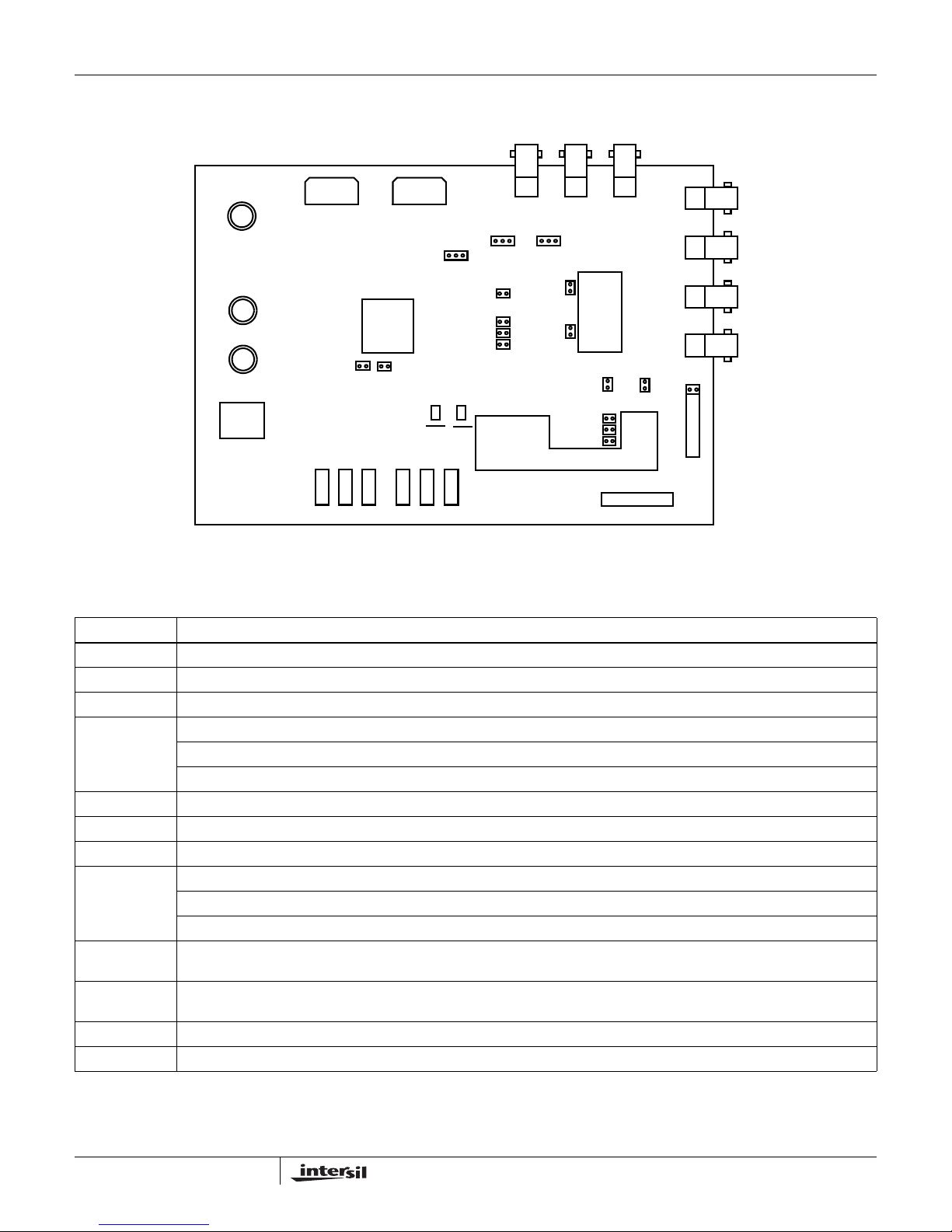
The evaluation board should have the same appearance as
shown in Figure 1.
RSLIC18™ is a trademark of Intersil Corporation.
CAUTION: These devices are sensitive to electrostatic discharge; follow proper IC Handling Procedures.
1-888-INTERSIL or 1-888-352-6832
| Intersil (and design) is a registered trademark of Intersil Americas Inc.
All other trademarks mentioned are the property of their respective owners.
Copyright Intersil Americas Inc. 2005. All Rights Reserved
Page 2
J4 - Gnd
J3 - Tip
J2 - Ring
J1
LOGIC 1
LOGIC 0
Application Note 1168
J5 J6
ISL5585
HC55185
RSLIC
JP1 JP2
POWER
LED
DET
POWER
SW+ SW-
S1 S2 S3 S4 S5 S6
F2 F1 F0 E0 SWC
JP13
Rx Gain
5V
3.3V
CODEC Rx
CODEC
Ext.
Trap.
LED
ALM
BSEL
J7- Vtx J8-Vrx
JP15
Hybrid Gain
Tx Gain
5V
3.3V
JP4
JP5
Ring
Signal
Source
CLOCK GENERATION
JP7
3.3V
JP9
A-law
PD
JP8
5V
W68131
W6810
CODEC
2.048 MHz
512 KHz
256 KHz
RSLIC Logic I/O
J9-Vrs
JP12
INT
JP10
J15
JP11
OLE
DROUT
J10
DT
J11
DR
J12
FS
J13
CLK
PCM I/O
J14
DRIN
FIGURE 1. EVALUATION BOARD LAYOUT
TABLE 1. EVALUATION BOARD JUMPER DEFINITIONS
JUMPER DESCRIPTION
JP1 Connects SW- directly to the RSLIC Ring terminal. Used in conjunction with external load D
JP2 Connects the SW+ D
diode + RTA resistor load to the RSLIC Tip terminal.
TA
and RTA.
TA
JP4 Connects the receive output of the CODEC (U6) to the RSLIC receive input (VRX). Path is AC coupled with CRX.
JP5 Position1, CODEC: Connects the CODEC receive output to the device ringing input. Path is AC coupled by C
Position 2, EXT: Connects the VRS connector J9 to the device ringing input. Path is AC coupled by C
RS
.
RS
.
Position 3 TRAP: Connects the VRS connector J9 thru RC network to the device ringing input. Path is AC coupled.
JP7 Selects the 5V or 3.3V chip-set Hybrid Gain of the CODEC, AC coupled by C
.
1
JP8 Inserting jumper sets the CODEC to A-law coding. Open sets the CODEC to µ-law coding.
JP9 Inserting jumper powers down the CODEC. Open provides normal CODEC operation.
JP10 Position 1: Sets the CODEC master clock to 2.048MHz when the internal clock generator is used.
Position 2: Sets the CODEC master clock to 512kHz when the internal clock generator is used.
Position 3: Sets the CODEC master clock to 256kHz when the internal clock generator is used.
JP11 Enables the on board clock generator. Should be installed for single board or back to back evaluations when no external clock
generation is available. Remove when driving BNCs J10 thru J13 with PCM4 or other PCM interface with external CLK.
JP12 Inserting jumper selects on board clock and frame sync generator. Insert to configure board as master for back to back
evaluations or for single board evaluations. Remove to configure board as slave for back to back evaluations.
JP13 Selects Rx Gain for 5V or 3.3V RSLIC/CODEC chip-set.
JP15 Selects Tx Gain for 5V or 3.3V RSLIC/CODEC chip-set.
2
January 24, 2005
Page 3
Application Note 1168
Po wer Requirements:
The multi-colored cable supplies the power from the external
supplies to the evaluation board through connector J5. For
complete channel testing with 2 evaluation boards, a
duplicate connector, J6, is provided to power the second
board from the first board using the white cable provided.
The evaluation board does not contain power supply
protection so care must be used to ensure that the power
supply connections and voltages are correct before applying
power.
Power supply tests points are provided on the evaluation
board.
External Power Supply Requirements
1. Vcc (red) and +5V (green): Vcc powers the RSLIC,
CODEC, LEDs and the on board clock generator. The
+5V supply provides the logic power to RSLIC control
switches S1 through S6. Both Vcc and +5V can be
powered from the same supply.
• HC55185/W6810: +5V @ 50mA per board and +5V.
• ISL5585/W68131: +3.3V @ 50mA per board.
2. Vbh (orange): RSLIC Ring voltage supply and surge
protection reference voltage (ISL5585 and HC55185)
• -70V to -100V DC@ 100mA per board; -100VDC
recommended
3. Vbl (yellow): RSLIC loop feed supply (ISL5585 and
HC55185)
• -19V to -60VDC @ 50mA per board; -28V
recommended
Line Card State Control
RSLIC Logic I/O Toggle Switches
Toggle switches S1 thru S6,control the logic I/O of the RSLIC
and are labeled with the control signal name.The RSLIC
operating modes are controlled by F2, F1, and F0 as shown
in Table 2.
The switch E0 selects the switch hook (E0 = 1) or the ground
key detector (E0 = 0) to appear at DET
device overrides E0 and sends the ring trip detector to DET
Switch SWC
logic low . Switch BSEL, selects the high battery when set to
logic high.
A logic I/O header, J15, is provided to enab le external digital
control of the RSLIC I/O. The logic switches should be set to
the center-off position when accessing the I/O through the
J15 header.
Refer to the specific RSLIC data sheet for detailed
description of operating states.
turns on the uncommitted switch when set to a
. During ringing, the
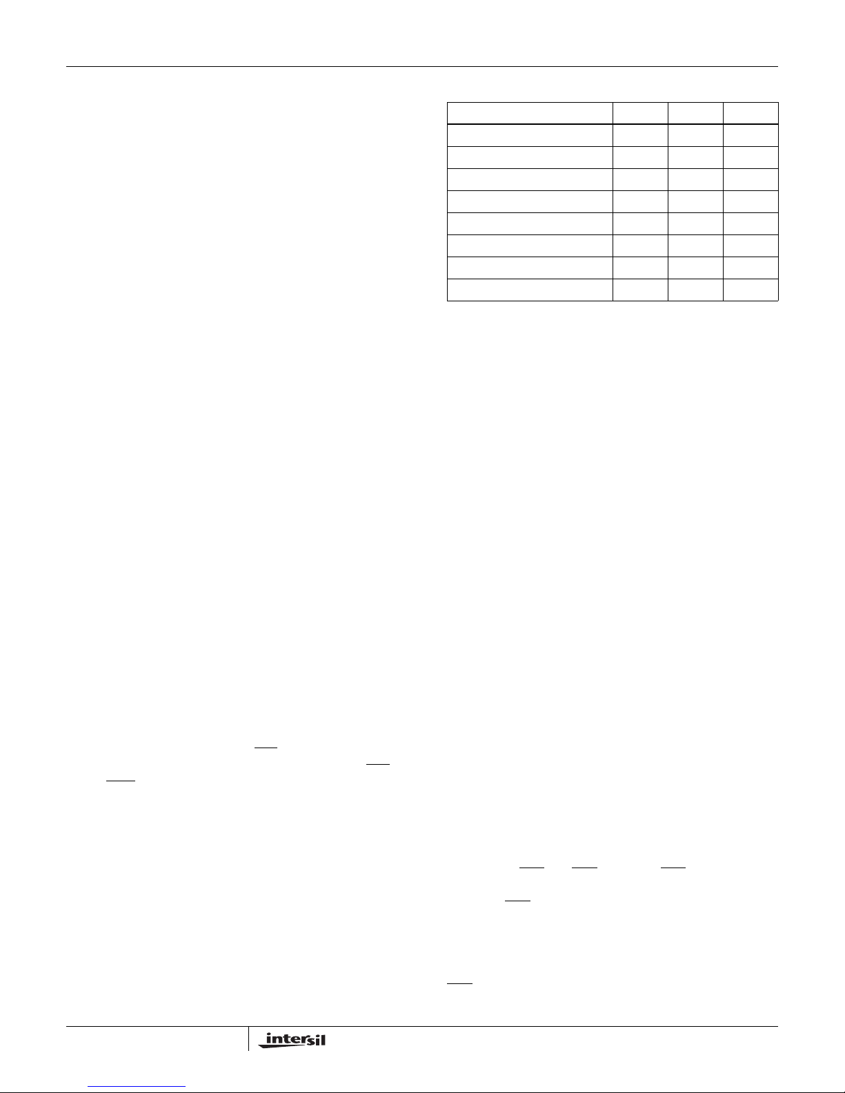
TABLE 2. RSLIC OPERATING MODES
OPERATING MODE F2 F1 F0
Low Power Standby 0 0 0
Forward Active 0 0 1
Unbalanced Ringing 0 1 0
Reverse Active 0 1 1
Ringing 1 0 0
Forward Loop Back (Note) 1 0 1
Tip Open 1 1 0
Power Denial 1 1 1
NOTE: The RSLIC should always operate from low battery voltage
when using the Forward Loop Back mode.
Single-Board Operation
Description
The stand alone configuration support s separate
measurement of the RSLIC or the CODEC. With all the
jumper locations open, the devices are isolated from each
other. All other circuitry is powered, but does not interfere
with SLIC or CODEC operation.
RSLIC Measurement Set-up
Access to the RSLIC analog 2W output ports is provided by
the Tip and Ring terminals, or the RJ11 jack. Test access to
the analog 4W and ring signal inputs is provided through the
VREC, VTX and VRS BNCs. Except for JP13, all jumper
positions should be open. Jumper JP13 is used to select the
RSLIC Rx gain depending on the RSLIC under test. The
logic control switches and RSLIC status LEDs are active.
RSLIC Measurement Capability
Nearly all AC and DC parameters of the SLIC can be
measured using this configuration. Typical RSLIC
measurements are listed below. The user should refer to the
device data sheet f or speci fic RSLIC parameter values.
1. RSLIC supply currents (CODEC removed).
2. Tip and Ring DC loop voltage and current measurements.
.
3. Ringing voltage and currents.
4. On hook, off-hook AC gains G
5. Other AC parameters such as longitudinal balance.
6. DC loop supervision and ring trip parameters.
, G24 and G44.
42
Status LEDs
Status LEDs DET and ALM are active. DET is illuminated in
response to a DC loop current in excess of the SHD
threshold. ALM
temperature exceeds the thermal shutdown temperature
threshold. This may happen during a tip or ring fault
condition, or if the Fwd Loopback is selected and BSEL is
high (to Vbh). Normal device operation should not cause the
ALM
indicator to light.
is illuminated whenever the IC internal
3
January 24, 2005
Page 4

Application Note 1168
TABLE 3. EVALUATION BOARD CONNECTOR DESCRIPTIONS
CONNECTOR DESCRIPTION
J1 RJ11 type phone connector.
J2 Ring terminal of board.
J3 Tip terminal of board.
J4 Grounding lug connected to board ground plane.
J5 1: V
J6 Identical pinout as J5. Either connector provides daisy chain connection to second board for back to back evaluation.
J7 Transmit analog output from the RSLIC device, VTX. This path is AC coupled and can be used to measure G2-4W of the RSLIC.
J8 Receive analog input to the RSLIC, VREC. This path is AC coupled and can be used to measure G4-2W of the RSLIC. Jumper
J9 Ringing input to HC55185 device, VRS. This path is AC coupled by C
J10 Serial transmit data output of CODEC U6.
J11 Serial receive data input to CODEC U6.
J12 Common frame sync input for receive and transmit digital data.
J13 Common clock for CODEC data transfer and conversion.
J14 20 pin, 100 mil spacing header with all digital PCM data interfaces to CODEC U6.
J15 20 pin, 100 mil spacing header with all digital interfaces to the RSLIC.
. Positive 5V supply to CODEC, RSLICU6, clock generator and logic devices (red wire).
CC
2: VBH. High negative battery supply to the HC55185 device (orange wire).
3: V
. Low negative battery supply to the HC55185 device (yellow wire).
BL
4: +5V. Positive 5V supply to the RSLIC LED detector output indicators (green wire).
7 thru 10: GND. Twisted pair returns for external supply connections (black wires).
The A-D Tx path of the CODEC can be measured using VTX as the signal input, but the RSLIC must be removed due to the
loading effect of the low impedance VTX output.
JP4 must be removed to disconnect the low impedance CODEC output. J8 can also be used to measure the D-A Rx gain of the
CODEC by re-inserting jumper JP4.
.
RS
CODEC Measurement Set-up
Test access to the CODEC digital I/O is provided by
connectors J10, J11, J12, and J13. Test access to the
CODEC analog ports is provided by inserting jumper JP4 to
connect the VREC connector to the CODEC analog Rx
output, and by inserting jumper JP15 to the correct Tx gain
setting for the CODEC under test. The RSLIC should be
removed during CODEC testing otherwise unwanted loading
of the CODEC analog Tx input signal could result. This setup is summarized in Table 8.
CODEC Measurement Capability
The user should refer to the device data sheet for correct
parameter values.
CODEC measurements include:
1. CODEC supply current (RSLIC removed).
2. A-D, D-A gain and frequency parameters.
3. A-law, mu-law companding measurements (JP8).
4. Power down measurements (JP9).
4
January 24, 2005
Page 5
Application Note 1168
SECTION 2: DC Functionality and AC Performance Testing
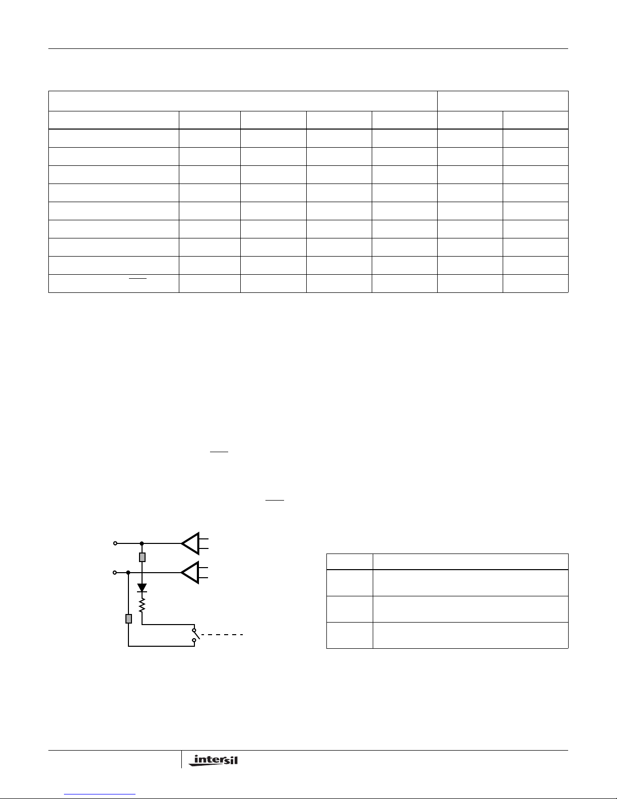
TABLE 4. EVALUATION BD. DC TEST VOLTAGES
Tip and Ring Voltages (Volts) - Tip to Ring Open Circuit; Vbl = -28V; Vbh = -100V DC Values (±20%)
OPERATING MODE F2, F1, F0 E0 SWC BSEL TIP TO GND RING TO GND.
Low Power Standby 0, 0, 0 x 1 1 -0.6V -49V
Forward Active 0, 0, 1 x 1 0 -4.0V -19.4V
Unbalanced Ringing 0, 1, 0 n/a n/a n/a -0.6V -50V
Reverse Active 0, 1, 1 x 1 0 -19.4V -4.0V
Ringing 1, 0, 0 x 1 1 -50V -50V
Forward Loop Back 1, 0, 1 x 1 0 -4.4V -19V
Tip Open 1, 1, 0 x 1 1 Float -49V
Power Denial 1, 1, 1 x 1 x Float Float
Uncommitted Switch (DET
LED on) 0, 0, 1 1 0 0 -12.4V -15.2V
DC Power-up Testing
After correct initial power-up, the DC tests measurements
shown in table 4 should be performed to verify proper
operation prior to performing the tests that follow.
Uncommitted Switch DC Test
When the jumpers JP1 and JP2 are installed, the
uncommitted switch is connected across Tip and Ring. The
test load of diode D
across the Tip and Ring terminals when the uncommitted
switch is turned on. The DC load will cause a DC loop
current flow at the loop current limit value of 25mA, resulting
in a switch hook detect indication by the DET
test load is a convenient method of checking the DC
operation of the RSLIC, howev er , operating the test load with
BSEL at Vbh (BSEL = 1) can cause excessive heating of the
RSLIC, causing thermal shutdown as indicated by the ALM
LED.
TIP
RING
and resistor RTA (100Ω) will connect
TA
LED. The DC
JP2
D
TA
R
TA
JP1
SW+
SW-
SWC
RSLIC Ringing Tests
Description
The ringing configuration supports full evaluation of the
ringing capability of the ISL5585 and HC55185 devices. The
evaluation board design does not include a ring signal
generator. Ring signals can be provided with an external
generator through the VRS BNC connector, or can be
sourced through the CODEC by inserting jumper JP5 CODEC.
Operation of the RSLIC in the ringing mode results in
dangerous voltages appearing at the tip and ring terminals.
Extra care is required when connecting external equipment
to the tip and ring terminals during testing to pre vent
personnel injury and equipment damage.
Jumper Settings
The jumper JP5 provides three positions for different ringing
techniques.
TABLE 5. JP5 JUMPER POSITIONS
JP5 POSN DESCRIPTION
CODEC Connects the CODEC receive output to the device
ringing input. Signal path is AC coupled.
EXT Connects the VRS connector J9 to the device ringing
input. Signal path is AC coupled.
TRAP Connects the VRS connector J9 thru RC network to
the device ringing input. Signal path is AC coupled.
FIGURE 2. TEST LOAD SWITCHING
5
CODEC Ringing
Most test equipment designed to evaluate the CODEC PCM
interface are capable of output frequencies as low as 20Hz.
If such a piece of equipment is available, then CODEC
ringing can be evaluated. The digital interface to the CODEC
is provided by the BNC connectors J10 thru J13. Verify JP11
January 24, 2005
Page 6
Application Note 1168
is open prior to driving signals into the BNC connectors. An
output level of 0dBm from the CODEC is required to provide
full scale ringing when operating from -100V battery.
External Ringing Source
Using an external function generator at J9 provides the most
control of the ringing waveform. The flexibility of the ringing
interface can be fully exercised by the function generator.
Trapezoidal Ringing
A logic level square wave, at J9, with 50% duty cycle will be
shaped by the components R
TRAP
and C
TRAP
when this
jumper position is selected. The components shipped with
the evaluation board will result in a 75V
trapezoidal
RMS
ringing waveform when operating from a -100V battery.
Ring Trip Control
Three very distinct actions occur when the device detects a
ring trip. First, the DET
output is latched low. The latching
mechanism eliminates the need for software filtering of the
detector output. The latch is cleared when the operating
mode is changed externally. Second, the VRS input is
disabled, removing the ring signal from the line. Third, the
device is internally forced to the forward active mode,
however, low battery is not automatically selected upon ring
trip, and must be switched manually using the BSEL toggle
switch.
AC Transmission Tests
Description
Tests of the AC transmission parameters of the SLIC and the
CODEC can be performed individually, or as a complete 2W
to PCM line circuit. Jumpers are used to complete the
analog signal interface between the RSLIC and the CODEC
as shown in Table 3. The RSLIC and CODEC gain equations
and target values are contained in Section 3: AC
Transmission Theory and Design.
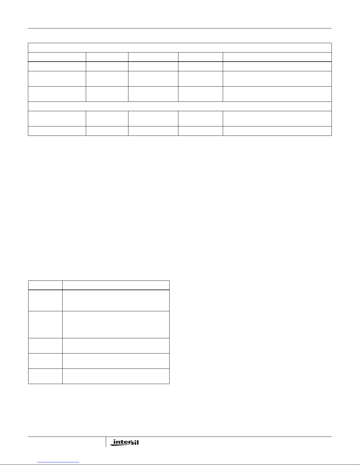
Test Set-up for RSLIC and CODEC Gains
Basic tests of the RSLIC and CODEC AC gain parameters
can be performed using a signal generator and standard AC
voltmeters, or a complete suite of PCM4 tests can be
performed on the RSLIC and the CODEC separately. The
RSLIC PCM4 tests use the A-A tests. The CODEC R
T
gain tests use the PCM4 A-D and D-A tests.
X
For RSLIC gain tests, the RX AC test input is connected to
the VREC BNC (RSLIC receive input) and the 2W AC test
output is measured at the tip-ring term inals. The RSLIC
analog 4W transmit output is measured at the VXMIT BNC.
A summary of RSLIC and CODEC tests is provided in Table
8.
The following analog input and output characteristics must
be considered when performing AC testing.
and
X
RSLIC analog I/O:
• Rx input impedance (VREC) is >30kΩ), and is AC
coupled.
• Tip to ring AC impedance is 600Ω. A DC potential of up
to 48VDC is present. AC coupling is required.
• Tx output impedance (at VXMIT) is <10Ω; AC coupled.
CODEC analog I/O
• Tx input (at VXMIT) is >50kΩ, DC coupled.
• Rx output (at VREC) is <20Ω, DC coupled.
Care must be given to the proper selection of analog
impedances on the PCM4 analog R
and TX ports when
X
performing PCM4 AC gain tests.
PCM4 Set-up
Analog PCM4 testing of the RSLIC parameters is performed
using the analog I/O on the front panel. CODEC A-D and DA testing with the PCM4 requires the use of the digital I/O
connections to the evaluation board as indicated in the table
below.
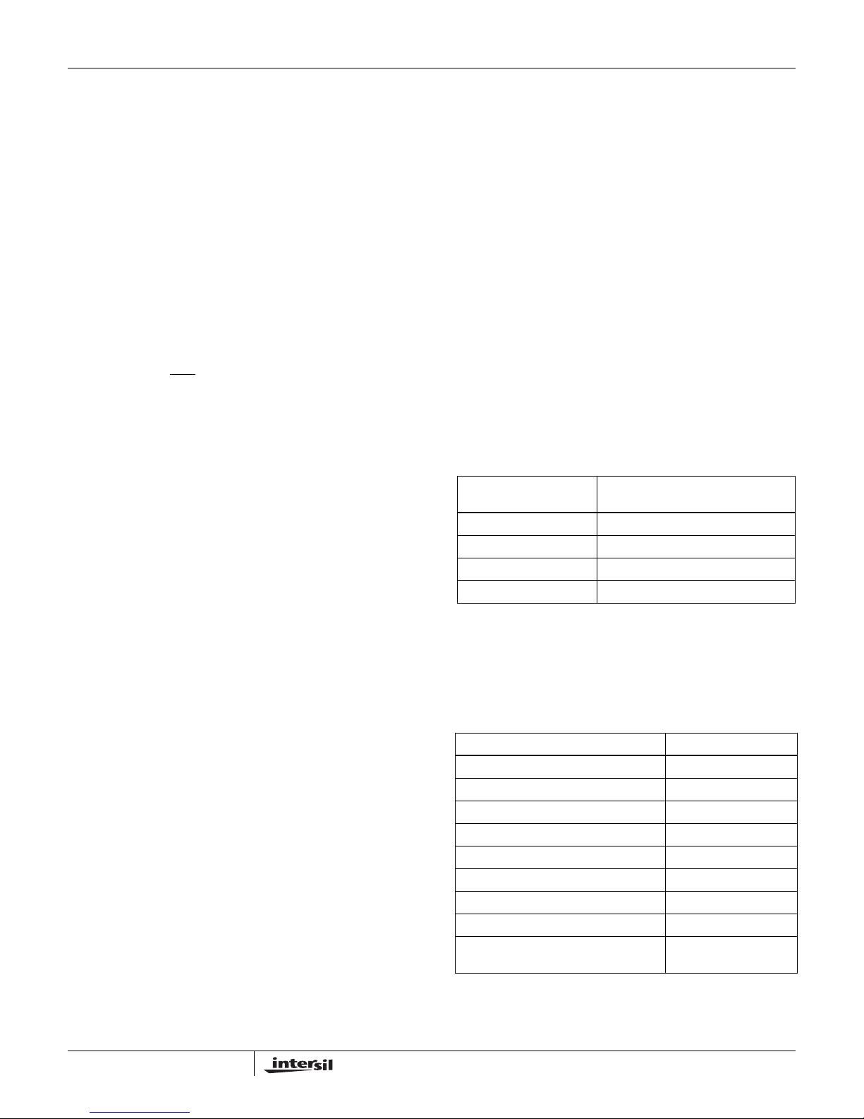
TABLE 6. PCM4 DIGITAL I/O CONNECTION
EVALUATION BOARD DIGITAL
PCM4 DIGITAL PORT
Rx Signal J10 - DT
Tx Signal J11 - DR
Frame Sync J12 - F.S.
Tx Clock J13 - CKL
Front panel cable lengths should be equal, and should be as
short as possible to prevent delay-induced errors.
The PCM4 General Parameter settings in the following table
should be used to configure the digital interface to the
CODEC prior to D-A and A-D testing.
TABLE 7. PCM4 GENERAL PARAMETER SETTINGS
PCM4 GENERAL PARAMETER SETTING
1 - DIGITAL CONFIGURATION 11, 23
2 - FRAME SELECTION 14, 24, 31
3 - DIGITAL TX INTERFACE 13, 22, 31
4 - DIGITAL RX INTERFACE 13, 22
5 - DIGITAL WORDS IN TX FRAME 11, 22
6 - TX ERROR INSERTION 11
7 - PCM ENCODING (A-law) 11, 21
8 - SCANNER PARAMETER 11, 21
9 - SPECIAL PARAMETER 11, 13, 16, 22, 23, 27,
PORT
33, 35
6
January 24, 2005
Page 7
Application Note 1168
TABLE 8. INDIVIDUAL TESTS OF THE RSLIC AND THE CODEC AC GAIN PATHS
RSLIC AC Testing - Jumper Selection (All jumpers removed except as indicated)
AC Test Install Jumpers AC Signal Input AC Signal Output Measurement Results and Remarks
G
42
G
44
G
24
CODEC AC Testing - Jumper Selection (All jumpers removed except as indicated)
Tx to PCM JP8 JP5(3.3V or 5V) VMXIT Remove RSLIC to prevent input loading; Measured
PCM to Rx JP4, JP8 PCM Tx digital input VREC Measured value per CODEC data sheet
None 0dB at VREC Tip to Ring Measured value per design tables A1 or B1
None 0dB at VREC VXMIT Insert 600Ω termination resistor from Tip to Ring;
Measured value per design tables A1 or B1
None 0dB at Tip/ring VXMIT Signal generator source impedance = 600Ω;
Measured value per design tables A1 or B1
value per CODEC data sheet
Half-channel A-D and D-A PCM4 Testing
Description
The evaluation board is designed for 0dB gain, PCM to 2W
(D-A, Rx) and 2W to PCM (A-D, Tx) transmission paths.
These gains are established by the RSLIC gain resistor
values on the evaluation board. The CODEC D-A and A-D
gains are fixed to the values defined in the specific CODEC
data sheet. A detailed description of the AC Transmission
gain paths and equations is provided in Section 3.
The PCM4 configuration verifies the AC A-D and D-A
transmission of the 5V or 3.3V RSLIC/CODEC chip-set. Any
piece of test equipment capable of PCM testing with digital
and analog interfaces can be used in this configuration.
Jumper Settings
All jumper settings and functions are described below. All
other jumpers should be removed.
TABLE 9. A-D AND D-A TEST JUMPER POSITIONS
JUMPER DESCRIPTION
JP4 Connects the receive output of the CODEC (U6) to
JP8 Inserting jumper set the CODEC to A-law coding.
JP13 Selects Rx Gain for 5V or 3.3V RSLIC/CODEC
JP15 Selects Tx Gain for 5V or 3.3V RSLIC/CODEC
JP7 Selects the 5V or 3.3V chip-set Hybrid Gain of the
the RSLIC receive input VRX. Signal path is AC
coupled.
Open sets the CODEC to µ-law coding. This must
match PCM test equipment coding scheme for
proper operation.
chip-set.
chip-set.
CODEC, AC coupled by C
.
1
FSR and FST, of the CODEC. These connections define
synchronous mode of operation.
Digital to Analog
The receive signal path is defined from the CODEC PCM
input to the RSLIC 2W Tip and Ring outputs . The PCM4 tester
is capable of driving digital test signals on the PCM bus and
measuring the resultant analog signal at Tip and Ring. Typical
performance measurements include overall lo ss , gain
variation versus frequency, gain versus signal lev el, THD and
2-wire return loss. In addition, fidelity measurements such as
idle channel noise and distortion may also be measured.
Analog to Digital
The transmit signal path is defined from RSLIC 2W Tip and
Ring interface to the CODEC PCM output. The same tests
performed for the receive path also apply to the transmit
path.
Digital to Digital
The digital to digital path is from the CODEC PCM input to
the CODEC PCM output. This signal path provides a
measure of the trans-hybrid balance for the line circuit with a
600Ω termination at Tip and Ring.
Digital Loop Back Configuration
Description
The digital loop back configuration can be used to verify the
interface and operation of the RSLIC/CODEC chip-set. This
configuration provides a convenient self -test in the Forward
or Reverse active states to verify proper operation of the
analog and digital functions of the line circuit. The on-board
clock generator eliminates the need for an external PCM4
digital interface, enabling testing with a signal generator, AC
voltmeter and scope.
Clock and Frame Sync
The clock and frame sync signals are driven at connectors
J13 and J12 respectively. The clock input is common to the
MCLK, BCLKT and BCLKR of the CODEC. The frame sync
input is common to the receive and transmit frame syncs,
7
NOTE: Operation of the clock oscillator and logic may be
marginal at VCC less than 3.3V.
January 24, 2005
Page 8
Application Note 1168
Digital Loop-back Jumper Settings
Jumper settings and functions are described in Table 10. All
other jumpers should be removed.
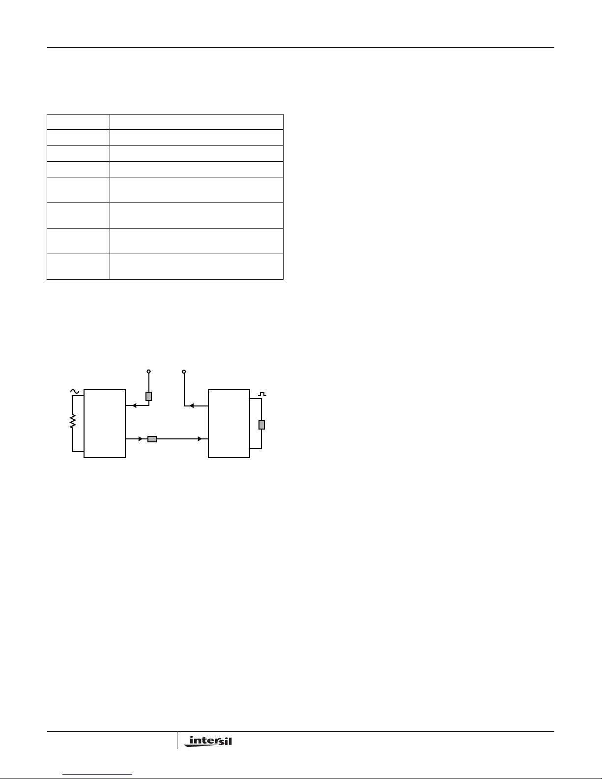
TABLE 10. DIGITAL LOOP BACK JUMPER POSITIONS
JUMPER DESCRIPTION
JP8 Optional - selects A-law or mu-law.
JP10, POSN 2 Sets the CODEC master clock to 512kHz.
JP11 Enables the on board logic multiplexer.
JP12 Inserting jumper selects on board clock and
frame sync generator.
JP13 Selects Rx Gain for 5V or 3.3V RSLIC/CODEC
chip-set.
JP15 Selects Tx Gain for 5V or 3.3V RSLIC/CODEC
J14, POSN 1
DROUT to DRIN
chip-set.
Connects the CODEC digital output DT to digital
input DR.
Digital Loopback Signal Flow
Driving a signal at VREC, J8, will result in a signal from the
CODEC receive output when the RSLIC is terminated at Tip
and Ring. The following diagram shows the signal path
formed by the jumpers and terminated SLIC.
VREC (J8)
JP4
3.3V ISL5585/CODEC Chip Set Digital Loop Back
Gain
For the 3.3V chip-set, EQ. 6 becomes:
•G
(3.3V Chip-set) = G44 (ISL5585) + G
DLB
and;
(CODEC),
TX
Substituting the G-values contained in the 3.3V AC
transmission model gives:
•G
(3.3V Chip-set) = 0.342dB + 2.71dB = 3.05dB
DLB
The 3.3V CODEC A-D gain is +5dB. Therefore the test AC
voltage at J8 should not exceed -5dB (~0.435 Vrms),
otherwise clipping may result. With a test signal of 0.1Vrms
@ 1kHz applied to J8, the output at JP4 should be 0.142
Vrms.
5V HC55185/CODEC Chip Set Digital Loop Back
Gain
For the 5V chip-set, EQ. 6 becomes:
• G(5V Chip-set) = G44 (HC55185)+ G
Substituting the G-values contained in the 5V AC
transmission model gives:
•G
(5V Chip-set) = -7.63dB + 7.63 dB = 0dB
DLB
With a test signal of 0.775Vrms @ 1kHz applied to J8, the
output at JP4 should be 0.322Vrms.
(CODEC), and;
TX
TIP
VRX
600Ω
VTX
RING
RSLIC CODEC
FIGURE 3. DIGITAL LOOP BACK SIGNAL FLOW
JP13
R
Select
JP15
T
Gain
X
Select
Gain
X
PO-
TG
DR
J14
DT
The measured gain from the from the AC input at VREC (J8)
to the AC signal output (JP4) is given by the following:
(EQ. 1) G
= G44 (RSLIC) +(GTX + G
DLB
A-D
+ G
)CODEC
D-A
where;
•G
•G
•(GTX is the gain set by the CODEC Tx amp gain resistors
•G
•G
is the digital loop-back gain,
DLB
is the RSLIC trans-hybrid gain,
44
is the CODEC TX absolute reference voltage level
A-D
is the CODEC RX absolute reference voltage level
D-A
The 5V and 3.3V CODECs have different A-D and D-A
gains, however, for both CODECs the A-D gain is equal to
the D-A gain so that these terms cancel each other . resulting
in:
(EQ. 2) G
= G44 (RSLIC) +GTX (CODEC)
DLB
The signal levels for digital loop back are independent of the
clock selected by JP10.
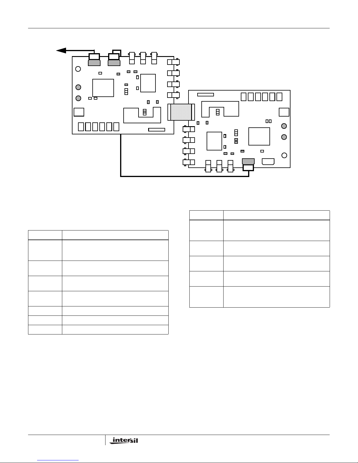
Dual-board A-A Configuration
Description
Two evaluation boards can be connected in the master-slave
configuration shown in Figure 4. The secondary power cable
provided connects power from the master board to the slave
board. The PCM digital communication interface is
established using a ribbon cable (not provided) connecting
the J14 connectors of each board.
This configuration establishes a full-duplex analog to analog
phone line across a common PCM bus. One board is
configured as a master for clock generation and the other is
configured as a slave. This PSTN-like configuration can be
used for speech communication between two phones, or to
perform full channel A-A PCM4 testing.
The ribbon cable used to connect the two boards at J14 also
connects the ground planes of the two evaluation boards.
Having returns adjacent to the high speed clock edges is
critical to reducing board level noise.
If transmission quality is poor verify both master and slave
boards are set up for same coding scheme, JP8. In addition,
verify the trans-hybrid jumper, JP7, is inserted in both
boards. If signal quality still does not improve, verify JP12 of
the slave board is not populated.
8
January 24, 2005
Page 9
POWER
SUPPLIES
Application Note 1168
MASTER
010x11
0
SECONDARY POWER CABLE
FIGURE 4. FULL CHANNEL A-A CONFIGURATION CONNECTORS AND JUMPERS
Dual-board A-A Jumper Settings
All jumper settings are described in Tables 11A and 11B. All
other jumpers should be removed.
TABLE 11A. MASTER BOARD JUMPER POSITIONS
JUMPER DESCRIPTION
JP4 Connects the receive output of the CODEC (U6) to
JP7 Selects the 5V or 3.3V chip-set Hybrid Gain of the
JP13 Selects Rx Gain for 5V or 3.3V RSLIC/CODEC
JP15 Selects Tx Gain for 5V or 3.3V RSLIC/CODEC
JP10, POSN 2 Sets the CODEC master clock to 512kHz.
JP11 Enables the on board logic multiplexer.
JP12 Configures board as master.
the RSLIC receive input VRX. Signal path is AC
coupled.
CODEC, AC coupled by C
.
1
chip-set.
chip-set.
01x1 00
SLAVE
TABLE 11B. SLAVE BOARD JUMPER POSITIONS
JUMPER DESCRIPTION
JP4 Connects the receive output of the CODEC (U6) to
the RSLIC receive input VRX. Signal path is AC
coupled.
JP7 Selects the 5V or 3.3V chip-set Hybrid Gain of the
CODEC, AC coupled by C
.
1
JP13 Selects Rx Gain for 5V or 3.3V RSLIC/CODEC
chip-set.
JP15 Selects Tx Gain for 5V or 3.3V RSLIC/CODEC
chip-set.
JP11 Configures the on board logic multiplexer to
receive MCLK and frame sync signals from the
master.
9
January 24, 2005
Page 10

Application Note 1168
SECTION 3: AC Transmission Theory and
Design
Introduction
The information in the next section describes the signal flow
of the RSLIC and CODEC PCM to 2W transmission circuits.
Appendices A and B contain the block diagrams and AC
transmission equations needed to tailor the AC transmission
parameters to specific user requirements.
The scope is limited to the design of the telephony T
R
voice circuits within the 0.3kHz to 3.4kHz frequency
X
band. The user should refer to the specific RSLIC and
CODEC data sheet design equations for all other BORSCHT
functions and performance parameters.
General Description (refer to Appendices A and B)
The evaluation board implements a complete half-channel
line circuit with the user’s choice of fixed gain 5V and 3.3V
CODECs interfaced to the appropriate RSLIC. The following
AC transmission parameters are set by resistors that control
the RSLIC transmission gain paths:
• 2W impedance
• Receive (R
• Transmit (T
• Transhybrid balance
The RSLIC and associated components implement a
voltage-feed, current-sense architecture for setting the
above parameters. The receive path begins as PCM code
input to the CODEC, which performs the D-A conversion at
fixed-gain and supplies the analog receive signal to the
RSLIC high impedance 4W V
amplifier has a fixed inverting voltage gain of -2 (voltagefeed) with a floating differential output at the Tip and Ring
terminals.
The G
24 Tx
input. The RSLIC provides a termination impedance to the
externally applied T
Ring terminals. A pair of series-connected current sense
resistors in the RSLIC are connected to a differential sense
amplifier that develops a voltage output proportional to the
sensed AC signal current. This voltage is applied to the noninverting input of a second amplifier whose output is
summed with the incoming Rx signal from the CODEC,
forming the impedance matching circuit. The gain of the
second stage is controlled with external feedback resistor
(Rs) allowing for adjustment of the level of feedback, and
therefore the RSLIC 2W synthesized impedance.
The HC55185 (5V) and ISL5585 (3.3V) RSLICs have the
same internal architecture, however, the G
are connected differently. The HC55185 G
Vrs, and the gain is fixed at 0dB. The ISL5585, however, is
required to compensate for the 3.3V CODEC attenuation
) D-A gain
X
) A-D gain
X
input. The RSLIC G42 Rx
rx
gain path begins at the RSLIC 2W tip and ring
signal appearing across the Tip and
x
42 Rx
42 RX
and
X
gain paths
input is at
(i.e. lower 0dBm0 reference level) with a gain increase. This
increase in R
R
output at the RSLIC second stage TX amplifier summing
X
gain is accomplished by injecting the CODEC
X
junction input through the external input resistor, Rin.
Connecting the RSLIC R
R
gain to be adjusted to any desired CODEC 0dBm0
X
reference level and any desired PCM to 2W R
HC55185 R
R
gains greater than 0dB are needed.
X
path my also be configured this way, if RSLIC
X
input in this fashion enables the
X
gain. The
X
The resistor component values used to set each AC
transmission parameter have a strong influence on the
remaining parameters. Therefore, an ordered approach is
required to complete the setting of all 4 AC transmission
parameters. These are described next in the correct order.
RSLIC 2W Impedance Matching
Correct matching of the RSLIC 2W terminal impedance with
the load impedance is a requirement before the R
gains can be set. There are 2 components that make up the
total RSLIC impedance; the protection resistors (2 X R
the synthesized terminal impedance of the RSLIC (Z
impedance matching circuit and design equations are
included in Appendices A and B and are identical for both
the HC55185 (Table A1) and the ISL5585 (Table B1).
The RSLIC synthesized impedance has a strong
dependence on the protection resistance Rp. When
performing the impedance calculation, the Rp term should
include all resistance elements in series with the RSLIC tip
and ring terminals. This is especially important when
resistive current limiting devices, such as PTCs, are used.
The evaluation board components provide a 600Ω
impedance using the on-board protection resistor values of
51Ω in the tip and ring leads.
Receive Gain Path, R
X
The D-A gain of the complete line circuit is the sum of the
CODEC D-A gain and the RSLIC G
42 RX
gain.
RX Gain for the 3.3V ISL5585 and 3.3V CODEC
The receive gain block diagram and equations for the 3.3V
ISL5585 and 3.3V CODEC are contained in Appendix A.
The receive gain path is defined by the following;
(EQ. 3) G
PCM - 2W
= GRX (CODEC) + G42 (RSLIC)
The 3.3V CODEC receive gain is fixed at -5dB and the
overall PCM to 2W gain is set by the ISL5585 RSLIC G
gain according to;
(EQ. 4) G42 =G
For a G
PCM-2W
- GRX (CODEC)
PCM-2W
receive gain equal to 0dB, the RSLIC RX
gain is given by:
(EQ. 5) G42 = 0dB -(-5dB) = 5dB
and TX
X
P
). The
O
42 RX
) and
10
January 24, 2005
Page 11

Application Note 1168
The ISL5585 RX gain equations are summarized in Table
A1, and should be used to calculate component values for
receive gains other than the 0dB level implemented on the
evaluation board.
R
Gain for the 5V HC55185 and 5V CODEC
X
The receive gain path block diagram and equations for the
5V HC55185 and 5V CODEC are contained in Appendix B.
The evaluation board is designed for an overall receive gain
of 0dB. The gain path equations (EQ. 8, and EQ. 9) apply to
this configuration. The evaluation board gain of 0dB and is
easily achieved due to the fixed 0dB gain of the RSLIC and
the CODEC.
For receive gains other than 0dB. the HC55185 R
gain path
X
can be configured to that of the ISL5585 as shown in
Appendix A. Both the ISL5585 and HC55185 are pincompatible, and have identical AC transmission gain blocks.
When using this alternate configuration with the HC55185,
the gain equations for the 3.3V configuration shown in Table
1A will apply.
The overall receive gain has a strong dependence on the
RSLIC synthesized impedance and the correct impedance
match.
Jumper JP13 selects the R
configuration and gain for the
X
ISL5585 and HC55185 RSLICs.
Transmit Gain Path, T
X
The transmit gain path circuits for both 3.3V and 5V are the
same. Howev er , the gain component values are different due
to differences in the Absolute V oltage Ref erence Le v el of the
3.3V and 5V CODECs. The transmit gain block diagram and
equations for the 3.3V ISL5585 and 3.3V CODEC are
contained in Appendix A.
The A-D gain of the complete line circuit is the sum of the
CODEC A-D gain and the RSLIC G
24 TX
gain.
The receive gain path is defined by the following;
(EQ. 6) G2W-PCM = G24 (RSLIC) + GTX (CODEC)
For the ISL:5585 and 3.3V CODEC, the TX gain needed for
an overall gain equal to 0dB is given by:
(EQ. 8) GTX (op amp) = 0dB - G24 (RSLIC) - G
0dB -(-7.63dB) -(5dB) = 2.63dB
(CODEC) =
A-D
For the HC55185 and the 5V CODEC, the TX gain needed
for an overall gain equal to 0dB is given by:
(EQ. 9) GTX (op amp) = 0dB - G24 (RSLIC) - G
0dB -(-7.63dB) -(0dB) = 7.63dB
(CODEC) =
A-D
The 3.3V and 5V RSLIC/CODEC TX gain equations are
summarized in Table A1 and B1 respectively; and should be
used to calculate transmit gains other than the 0dB
implemented on the evaluation board.
The overall transmit gain has a strong dependence on the
RSLIC synthesized impedance and the correct impedance
match.
Jumper JP15 selects the T
gain for the ISL5585 and
X
HC55185 RSLICs.
Trans-hybrid Balance
The trans-hybrid balance network is implemented at the
CODEC Tx amplifier summing input. The network consists of
a pair of resistors that sum the 180
signal from Vtx, with the CODEC Rx signal. The magnitude
of the 4W return signal relative to the CODEC Rx output is
equal to the RSLIC G
trans-hybrid gain. Therefore,
44
complete 4W return signal cancellation occurs when the
trans-hybrid resistor pair ratio produces a gain equal to G
as shown in the Hybrid Model diagrams contained in
Appendices A and B.
Trans-hybrid balance performance can be tested using the
PCM4 A11 D-D level test with a 600Ω termination at the tip
and ring terminals. The echo-return loss is typically greater
than 23dB.
Jumper JP7 selects the proper transhybrid gain for the
RSLIC/CODEC chip-set used.
o
out of phase RSLIC 4W
44
The 3.3V and 5V RSLICs have the same TX gain which is
fixed at -7.63dB. The CODEC transmit gain path contains 2
gain blocks. An internal T
resistors feeds the internal T
op-amp with external gain setting
X
A-D converter. The A-D
X
converter has a fixed conversion gain needed to restore the
CODEC Absolute Voltage Reference Level to the 0dBm0
standard value of 0.775Vrms at 600Ω, at the PCM bus. The
overall line circuit 2W to PCM gain is adjusted using the gain
resistors at the input to the CODEC T
op amp.
X
The 2W - PCM gain is defined by the following:
(EQ. 7) G
(CODEC)
= G24 (RSLIC) + GTX (op amp) + G
2W-PCM
11
A-D
Trans-hybrid balance has a strong dependence on RSLIC
impedance matching and accurate T
and RX gains. In
X
practice, minor deviations from the design value may occur
due to resistor value rounding to the closest standard value.
January 24, 2005
Page 12
Application Note 1168
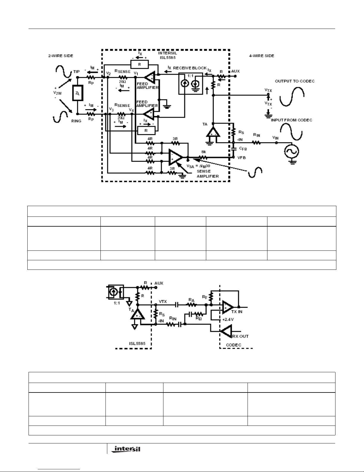
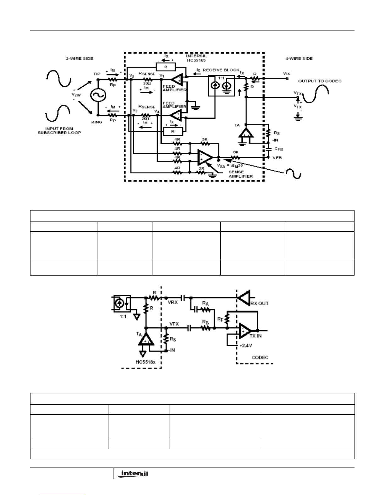
APPENDIX A: ISL5585 3.3V AC Transmission Model and Design Equations
FIGURE A1: ISL5585 AC TRANSMISSION BLOCK DIAGRAM
TABLE A1: ISL5585 IMPEDANCE MATCHING AND GAIN EQUATIONS
ISL5585/W68131: CODEC 0dBm0 Absolute Voltage Reference Level = -5dB (0.436Vrms)
Transmission Parameter ZO = ZL - 2R
P
AC Gain Equations
RS
Z
-------------- -= G
O
133.3
Eval. Board Values Z
= 499Ω G42 = +5dB G24 = -7.63dB G44 = 0.342dB
O
Eval. Board Component Values: Rp = 51Ω; Rs = 66.5kΩ; Rin = 37.4kΩ;
FIGURE A2: ISL5585 HYBRID BLOCK DIAGRAM
TABLE A2: ISL5585 TRSANS-HYBRID BALANCE EQUATIONS
G
42
Rs
---------=
42
Rin
G
24
G
24
Z
–=
O
---------------------------------------
ZO2RPZ
++
L
G
44
Rs
ZL 2RP+
---------------------------------------
G
---------
–=
44
++
Rin
Z
L2RPZO
ISL5585/W68131 Hybrid Gain: CODEC 0dBm0 Absolute Voltage Reference Level = -5dB (0.436Vrms)
Hybrid Parameter Transmit Gain (GTX) Transhybrid Gain (G44) Transhybrid Balance G
AC Gain Equations
G
Eval. Board Values: G
Eval. Board Component Values: Rp = 51Ω
12
= 1.366 = 2.71dB G44 = 0.342dB G
TX
Rs
RF
--------=
TX
RA
; Rs = 66.5kΩ; RA = 73.2kΩ; RB = 69.8kΩ, RF = 100kΩ
–=
G
44
ZL 2RP+
---------------------------------------
---------
++
Rin
Z
L2RPZO
G
G44
THB
= 1.049 = 0.413dB
THB
THB = G44
RA
--------==
RB
January 24, 2005
Page 13
Application Note 1168
APPENDIX B: HC55185 5V AC Transmission Model and Design Equations
FIGURE B1: HC55185 AC TRANSMISSION BLOCK DIAGRAM
TABLE B1: HC55185 IMPEDANCE MATCHING AND GAIN EQUATIONS
HC55185 AC Transmission Gains (dB), 600Ω, 0dBm0 reference level = 0dB (0.775Vrms
Transmission Parameter ZO = ZL - 2R
AC Gain Equations
RS
Z
-------------- -= G
O
133.3
Eval. Board Values:
Rp = 51Ω
Rs = 66.5kΩ
= 499Ω G42 = 0dB G24 = -7.63dB G44 =0.416 = -7.63dB
Z
O
TABLE B2: HC55185 TRANS HYBRID BALANCE EQUATIONS
P
42
FIGURE B2: HC55185 HYBRID BLOCK DIAGRAM
G
42
Z
–=
2
L
---------------------------------------
ZL2RPZ
++
G
24
O
G
24
Z
O
---------------------------------------
–=
ZO2RPZ
++
L
G
44
Z
O
---------------------------------------
–=
G
44
ZL2RPZ
++
O
HC55185/W6810: Hybrid Gain: A-D Gain = D-A Gain = 0dB; 0dBm0 reference le vel = 0dB (0.775Vrms)
Hybrid Parameter Transmit Gain (GTX) Transhybrid Gain (G44) Transhybrid Balance G
AC Gain Equations
G
Eval. Board Values: G
Eval. Board Component Values: Rp = 51Ω
13
RF
--------=
TX
RB
= 2.427 G44 = -7.63dB G
TX
; Rs = 66.5kΩ; RA = 100kΩ; RB = 41.2kΩ, RF = 100kΩ
–=
G
44
Z0
---------------------------------------
2RPZ
++
Z
L
O
G
THB
G44
= -7.63dB
THB
THB = G44
RB
--------==
RA
January 24, 2005
Page 14
14
January 24, 2005
Application Note 1168
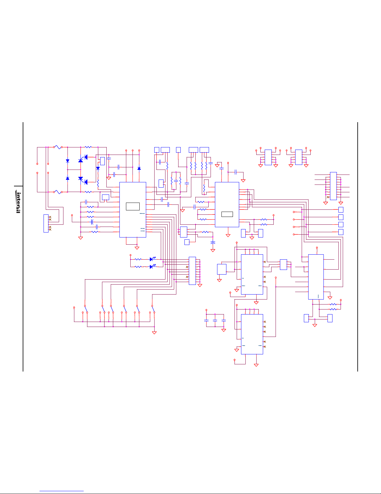
ISL5585EVAL4 Schematic
PWR CONN
-24V
-72 to -100V
CRX
0.4uF
CODEC
CFB0.47uF
123
JP13
RP
0 Ohm 1%
RS66.5K 1%
123
JP15
CTX0.47uF 20%
12
3
B1100CC - TECCOR
Q1
SEL
1
1A
2
1B
3
1Y
4
2A
5
2B
6
2Y
7
3A
11
3B
10
4A
14
4B
13
3Y
9
4Y
12
OE
15
VCC
16
GND
8
U4
74HC257
P1
1
Q1
2
Q0
3
CE
4
U/D
5
Q2
6
Q3
7
PL
11
P2
10
CP
14
RC
13
P3
9
TC
12
P0
15
VCC16GND
8
U3
74HC191
P1
1
Q1
2
Q0
3
CE
4
U/D
5
Q2
6
Q3
7
PL
11
P2
10
CP
14
RC
13
P3
9
TC
12
P0
15
VCC16GND
8
U2
74HC191
VCC
14
OUT
8
GND
7
U5
X0-43B
1 2
3 4
5 6
JP10
RTA
100 Ohm 1%
VCC
1 2
3 4
5 6
7 8
9 10
J6
1 2
3
4
5 6
7 8
9 10
J5
2.048Mhz
512kHz
256kHz
VCC
TIP
RING
VCC
VBL
VCC VBH
+5V
RX
GAIN
TX
GAIN
HYBRID
GAIN
DR_IN
FS_CNT
CLK_IN
FS_IN
VCC
VBL
1
FS_CNT
+5V
+
CDC 4.7uF
VBH
C6
0.1uF
C5
0.1uF
C4
0.1uF
VCC
1
2
JP11
B2B OLE
1
2
JP12
MASTER INT
R12
10k 1%
R13
10K 1%
VCC
1 2
3 4
5 6
7 8
9 10
1112
1314
1516
1718
1920
J14
CLK_IN
DR_IN
FS_IN
DR_IN
FS_OUT
DT_OUT
CLK_OUT
1 2
3 4
5 6
7 8
9 10
1112
1314
1516
1718
1920
J15
R1 499 Ohm 1%
R2 499 Ohm 1%
A\L\M\
BSEL
D\E\T\
F1
F2
E0
F0
S\W\C\
DTA
BAS21ZXCT
VCC
VDD
6
VSS
15
PUI
10
u/A
16
FST
14
BCLKT
12
PCMT
13
MCLK
11
PCMR
8
BCLKR
9
FSR
7
AO
17
AI-
18
AI+
19
VAG
20
VREF
1
RO-
2
PAO+
5
PAI
3
PAO-
4
U6
VBL
+5V
CPS1
0.1uF 20V
CR3
1N4007
RTL
18.7K
1
2
3
4
5
6
J1
RJ11
DR
1
2
JP1 TEST
R7
100K
CLK_OUT
C2
0.1uF 6.3V
FS_OUT
RRT 23.7K
Dual
Banana
Jack
Test Points
CAG
0.01uF
VBH
SLIC
1
1
J11
RP2 49.9 ohms
1
1
J13
1
1
J12
1
1
J10
1
FS
1
DR
1
DT
1
CLK
1
2
JP9
PD
1
2
JP8
A-LAW
CRT 0.47uF
VCC
F2
TECCOR F1250T
RING
CR1 LED
0.47uFCPOL
CR2 LED
R10 10k 5%
VCC
TIP
1
2
JP2
TEST
R11 10k 5%
CPS3
0.1uF 6.3V
VCC
TIP
1
BGND
2
VBL
3
VBH
4
SW+
5
SW-
6
SWC
7
F2
8
F1
9
F0
10
E0
11
DET
12
ALM
13
AGND
14
BSEL
15
TL
16
POL
17
VRS
18
VRX
19
VTX
20
VFB
21
IN-
22
VCC
23
CDC
24
RTD
25
ILIM
26
RD
27
RING
28
U1
HC55185 or
ISL5585
RSH 49.9 K
R6 10k 1%
R5 10k 1%
CPS2
0.1uF 200V
RIL 71.5K
F1
TECCOR F1250T
C1
0.1uF
1 2
3 4
5 6
JP5
+
CTRAP
0.47uF 20% 20V
RTRAP 20K 1%
VCC
VCC
S6
S6-S1 (ON-OFF-ON)
S1 S2
VCC
RP1 49.9 ohms
TRAP
S3
S4
1
1
J9
S5
123
JP7
Cref
0.1uF 6.3V
R3A100K 1%
R3B69.8 1%
W6810 or
W68131
R4B
41.2K 1%
R4A
73.2K 1%
DT_OUT
R8
10K 1%
CRS 0.47uF
BSEL
F0
F1F2
SWCE0
1
2
JP4
CODEC
5v 3.3v
3.3v
5v
5v
RIN
37.4K 1%
CP?
1 2
3
B1100CC - TECCOR
Q2
CR41N4935
CR51N4935
1
1
J7 VXMIT
1
1
J8 VREC
PWR CONN
-24V
-72 to -100V
CRX
0.4uF
CODEC
CFB0.47uF
123
JP13
RP
0 Ohm 1%
RS66.5K 1%
123
JP15
CTX0.47uF 20%
12
3
B1100CC - TECCOR
Q1
SEL
1
1A
2
1B
3
1Y
4
2A
5
2B
6
2Y
7
3A
11
3B
10
4A
14
4B
13
3Y
9
4Y
12
OE
15
VCC
16
GND
8
U4
74HC257
P1
1
Q1
2
Q0
3
CE
4
U/D
5
Q2
6
Q3
7
PL
11
P2
10
CP
14
RC
13
P3
9
TC
12
P0
15
VCC16GND
8
U3
74HC191
P1
1
Q1
2
Q0
3
CE
4
U/D
5
Q2
6
Q3
7
PL
11
P2
10
CP
14
RC
13
P3
9
TC
12
P0
15
VCC16GND
8
U2
74HC191
VCC
14
OUT
8
GND
7
U5
X0-43B
1 2
3 4
5 6
JP10
RTA
100 Ohm 1%
VCC
1 2
3 4
5 6
7 8
9 10
J6
1 2
3
4
5 6
7 8
9 10
J5
2.048Mhz
512kHz
256kHz
VCC
TIP
RING
VCC
VBL
VCC VBH
+5V
RX
GAIN
TX
GAIN
HYBRID
GAIN
DR_IN
FS_CNT
CLK_IN
FS_IN
VCC
VBL
1
FS_CNT
+5V
+
CDC 4.7uF
VBH
C6
0.1uF
C5
0.1uF
C4
0.1uF
VCC
1
2
JP11
B2B OLE
1
2
JP12
MASTER INT
R12
10k 1%
R13
10K 1%
VCC
1 2
3 4
5 6
7 8
9 10
1112
1314
1516
1718
1920
J14
CLK_IN
DR_IN
FS_IN
DR_IN
FS_OUT
DT_OUT
CLK_OUT
1 2
3 4
5 6
7 8
9 10
1112
1314
1516
1718
1920
J15
R1 499 Ohm 1%
R2 499 Ohm 1%
A\L\M\
BSEL
D\E\T\
F1
F2
E0
F0
S\W\C\
DTA
BAS21ZXCT
VCC
VDD
6
VSS
15
PUI
10
u/A
16
FST
14
BCLKT
12
PCMT
13
MCLK
11
PCMR
8
BCLKR
9
FSR
7
AO
17
AI-
18
AI+
19
VAG
20
VREF
1
RO-
2
PAO+
5
PAI
3
PAO-
4
U6
VBL
+5V
CPS1
0.1uF 20V
CR3
1N4007
RTL
18.7K
1
2
3
4
5
6
J1
RJ11
DR
1
2
JP1 TEST
R7
100K
CLK_OUT
C2
0.1uF 6.3V
FS_OUT
RRT 23.7K
Dual
Banana
Jack
Test Points
CAG
0.01uF
VBH
SLIC
1
1
J11
RP2 49.9 ohms
1
1
J13
1
1
J12
1
1
J10
1
FS
1
DR
1
DT
1
CLK
1
2
JP9
PD
1
2
JP8
A-LAW
CRT 0.47uF
VCC
F2
TECCOR F1250T
RING
CR1 LED
0.47uFCPOL
CR2 LED
R10 10k 5%
VCC
TIP
1
2
JP2
TEST
R11 10k 5%
CPS3
0.1uF 6.3V
VCC
TIP
1
BGND
2
VBL
3
VBH
4
SW+
5
SW-
6
SWC
7
F2
8
F1
9
F0
10
E0
11
DET
12
ALM
13
AGND
14
BSEL
15
TL
16
POL
17
VRS
18
VRX
19
VTX
20
VFB
21
IN-
22
VCC
23
CDC
24
RTD
25
ILIM
26
RD
27
RING
28
U1
HC55185 or
ISL5585
RSH 49.9 K
R6 10k 1%
R5 10k 1%
CPS2
0.1uF 200V
RIL 71.5K
F1
TECCOR F1250T
C1
0.1uF
1 2
3 4
5 6
JP5
+
CTRAP
0.47uF 20% 20V
RTRAP 20K 1%
VCC
VCC
S6
S6-S1 (ON-OFF-ON)
S1 S2
VCC
RP1 49.9 ohms
TRAP
S3
S4
1
1
J9
S5
123
JP7
Cref
0.1uF 6.3V
R3A100K 1%
R3B69.8 1%
W6810 or
W68131
W6810 or
W68131
R4B
41.2K 1%
R4A
73.2K 1%
DT_OUT
R8
10K 1%
CRS 0.47uF
BSEL
F0
F1F2
SWCE0
1
2
JP4
CODEC
5v 3.3v
3.3v
5v
5v
RIN
37.4K 1%
CP?
1 2
3
B1100CC - TECCOR
Q2
CR41N4935
CR51N4935
1
1
J7 VXMIT
1
1
J8 VREC
Page 15
Application Note 1168
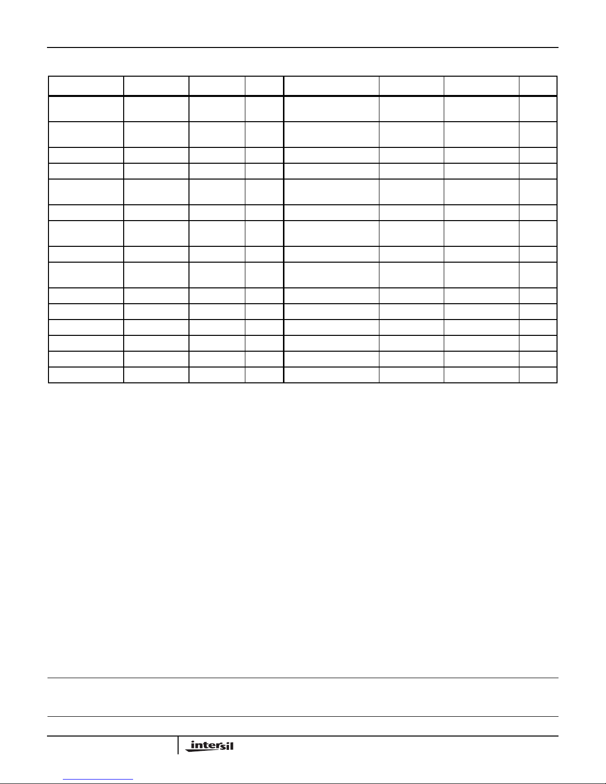
ISL5585EVAL4 Electrical Component List
COMPONENT VALUE TOLERANCE RATING COMPONENT VALUE TOLERANCE RATING
U
- Ringing SLIC HC55185 (5V) or
1
U
, U
2
3
U
4
U
5
U
CODEC W6810 (5V), or
6-
F
, F2 - Fuse F1250T TECCOR N/A RTL 17.8kΩ 1% 0.10W
1
Q
, Q2 - Surge
1
Protector
R
, R
RT
TRAP
R
SH
R
IL
R
TA
R
S
R
P
R
, R
1
2
R
, R
3A
7
ISL5585 (3.3V)
74HC191M N/A N/A R5, R6, R8, R10, R11,
74HC257M N/A N/A R14, R15 51Ω 5%, picked to 0.1Ω 0.50W
XO-43B N/A N/A R4A 44.2kΩ 1% 0.10W
W68131 (3.3V
B1100CC TECCOR N/A CFB, CRT, CRX, CRS,
20kΩ 1% 0.10W CDC, 4.7µF 20% 20V
49.9kΩ 1% 0.10W CPS1, CPS2, CPS3,
71.5kΩ 1% 0.10W C2, C3, C4, C5, C6 0.1µF 20% 20V
100Ω 1% 0.25W CR1, CR2 LN1251C N/A N/A
66.5kΩ 1% 0.10W CR3 DL4003CT-ND N/A N/A
0Ω 1% 0.10W CR4, CR5 Diode, 200V, 1A 1N4935
499Ω 1% 0.10W DTA BAS21ZXCT N/A N/A
100kΩ 1% 0.10W
Intersil Corp. N/A R3B 69.8kΩ 1% 0.10W
10kΩ 1% 0.10W
R12, R13
Winbond USA N/A R4B 73.2kΩ 1% 0.10W
0.47µF 20% 20V
CTX, C1, CPOL, CTRAP
0.1µF 20% 100V
CPS4, CPS5
All Intersil U.S. products are manufactured, assembled and tested utilizing ISO9000 quality systems.
Intersil Corporation’s quality certifications can be viewed at www.intersil.com/design/quality
Intersil products are sold by description only. Intersil Corporation reserves the right to make changes in circuit design, software and/or specifications at any time without
notice. Accordingly, the reader is cautioned to verify that data sheets are current before placing orders. Information furnished by Intersil is believed to be accurate and
reliable. However, no responsibility is assumed by Intersil or its subsidiaries for its use; nor for any infringements of patents or other rights of third parties which may result
from its use. No license is granted by implication or otherwise under any patent or patent rights of Intersil or its subsidiaries.
For information regarding Intersil Corporation and its products, see www.intersil.com
15
January 24, 2005
 Loading...