

Page 1
®
www.BDTIC.com/Intersil
ISL5571A
Data Sheet July 2004
Access High Voltage Switch
The ISL5571A is a solid state device designed to replace the
electromechanical relay used on Subscriber Line Cards. The
device contains two Line Break MOSFET switches, one Ring
Return MOSFET switch and one Ring Access SCR switch.
The ISL5571A is pin-for-pin compatible with the Lucent
L7581AAE LCAS and Clare CPCL7581A Products.
Improvements include: line break switches r
match (0.5Ω
ON
Max) higher dV/dt sensitivity (5000V/µs), protection SCR
hold current set to 110mA.
The line break MOSFETs have very low on resistance
(<16.0Ω Typ) and Ron match (<0.05Ω Typ, 0.5Ω Max) and a
blocking voltage >330V. The Ring Return MOSFET has a
typical Ron of 50Ω and a blocking voltage >330V. The
Ringing Access switch is implemented with a SCR device
with a blocking voltage >480V. The SCR switch inherently
offers low EMI connect and disconnect circuitry. All control
I/Os use TTL thresholds making the device compatible with
3V logic.
The ISL5571A also includes on-chip protection in the form of
an over-voltage clamping circuit, current-limited MOSFET
switches, and thermal shutdown circuitry. The over-voltage
clamping circuit consists of a diode bridge and SCR.
Ordering Information
PART
NUMBER
ISL5571AIB Yes -40 to 85 16 Ld SOIC M16.3
ISL5571AIBZ
(Note)
NOTE: Intersil Pb-free products employ special Pb-free material
sets; molding compounds/die attach materials and 100% matte tin
plate termination finish, which is compatible with both SnPb and
Pb-free soldering operations. Intersil Pb-free products are MSL
classified at Pb-free peak reflow temperatures that meet or exceed
the Pb-free requirements of IPC/JEDEC J Std-020B.
Add “-T” for tape and reel.
PROT
SCR
Yes -40 to 85 16 Ld SOIC
TEMP
RANGE (°C)
PACKAGE
TYPE
(Pb-free)
PKG.
DWG. #
M16.3
FN4920.5
Features
• Small Size/Surface-Mount Packaging
• Low Impulse Noise, Low EMI
• Clean, Bounce-Free Switching
• Line Break Switches
-0.5Ω Max r
-28Ω Max r
ON
ON
Match
• Built-In Current Limiting, Thermal Shutdown and
Secondary Protection for the SLIC
• Optimized for Short Loop High REN Applications
• 3V/5V Logic-Capable I/O
• Pb-free Available
Applications
• Central Office
• PBX
•DLC
•HFC
•FITL
•DAML
Related Literature
• Technical Brief TB363 “Guidelines for Handling and
Processing Moisture Sensitive Surface Mount Devices
(SMDs)”
• Technical Brief TB379 “Thermal Characterization of
Packages for ICs”
• Texas Instruments TISPL758LF3D Data Sheet
• Teccor Electronics Document DO-214AA
Pinout
ISL5571A
TOP VIEW
1
CAUTION: These devices are sensitive to electrostatic discharge; follow proper IC Handling Procedures.
1-888-INTERSIL or 321-724-7143
| Intersil (and design) is a registered trademark of Intersil Americas Inc.
Copyright © Intersil Americas Inc. 2001, 2002, 2004. All Rights Reserved
All other trademarks mentioned are the property of their respective owners.
F
T
T
T
GND
BAT
LINE
NC
NC
RING
V
DD
T
SD
16
15
14
13
12
11
10
9
V
BAT
R
BAT
R
LINE
NC
R
RING
LATCH
INPUT
D
GND
1
2
3
4
5
6
7
8
Page 2
Block Diagram
www.BDTIC.com/Intersil
T
R
LINE
LINE
3
14
T
RING
6
RING
RETURN
SW3
RING
ACCESS
SW4
ISL5571A
ISL5571A - 16 LEAD SOIC
LINE BREAK
SW1
D1
D2
LINE BREAK
SW2
D3
D4
CONTROL LOGIC
V
BAT
16
SCR
2
T
BAT
1
F
GND
R
15
BAT
V
7
DD
12 11 10 8
R
RING
INPUTLATCH
D
9
GND
TSD
2
Page 3
ISL5571A
www.BDTIC.com/Intersil
Absolute Maximum Ratings T
Maximum Supply Voltages
(V
) . . . . . . . . . . . . . . . . . . . . . . . . . . . . . . . . . . . . .-0.5V to +7V
DD
) . . . . . . . . . . . . . . . . . . . . . . . . . . . . . . . . . . .-19V to -100V
(V
BAT
ESD Rating (Human Body Model). . . . . . . . . . . . . . . . . . . . . . .500V
Die Characteristics
Substrate Potential. . . . . . . . . . . . . . . . . . . . . . . . . . . . . . . . . . V
Process . . . . . . . . . . . . . . . . . . . . . . . .6-inch BIMOS Bonded Wafer
CAUTION: Stresses above those listed in “Absolute Maximum Ratings” may cause permanent damage to the device. This is a stress only rating and operation of the
device at these or any other conditions above those indicated in the operational sections of this specification is not implied.
NOTE:
is measured with the component mounted on a low effective thermal conductivity test board in free air. See Tech Brief TB379 for details.
1. θ
JA
Electrical Specifications T
PARAMETER TEST CONDITION MEASURE MIN TYP MAX UNITS
OFF-State Leakage Current:
ON-Resistance:
ON-Resistance Match Per ON-resistance Test Condition of SW1, SW2 Magnitude
ON-State Voltage (Note 2) Break Switches in ON-State; I
DC Current Limit:
Dynamic Current Limit
(t = <0.5µs)
Isolation:
dV/dt Sensitivity (Note 3) - 5000 - V/µs
NOTES:
2. Choice of secondary protection should ensure this rating is not exceeded.
3. Applied voltage is 100V
-40°C
25°C
85°C
-40°C
25°C
85°C
-40°C
25°C
85°C
-40°C
25°C
85°C
V
V
V
V
V
V
T
T
T
50/60Hz
V
V
V
Break Switches in ON-state; Ringing Access
Switches OFF; Apply ±1000V at 10/1000µs
Pulse; Appropriate External Secondary
Protection in Place
V
Logic Inputs = GND
V
Logic Inputs = GND
V
Logic Inputs = GND
square wave at 100Hz.
P-P
= 25°C Thermal Information
A
Thermal Resistance (Typical, Note 1) θ
SOIC . . . . . . . . . . . . . . . . . . . . . . . . . . . . . . . . . . . . 100
Maximum Junction Temperature Plastic . . . . . . . . . . . . . . . . .150
Maximum Storage Temperature Range . . . . . . . . . -65
Maximum Lead Temperature (Soldering 10s). . . . . . . . . . . . .300
(SOIC - Lead Tips Only)
BAT
= -40°C to 85°C, Unless Otherwise Specified
A
TABLE 1. BREAK SWITCHES - ISL5571A - SW1, SW2
at
I
SWITCH
I
SWITCH
I
SWITCH
∆V
ON
∆V
ON
∆V
ON
SW1 - rON SW2
r
ON
V
ON
I
SWITCH
I
SWITCH
I
SWITCH
I
SWITCH
I
SWITCH
I
SWITCH
I
SWITCH
SWITCH (DIFFERENTIAL)
SWITCH (DIFFERENTIAL)
SWITCH (DIFFERENTIAL)
SWITCH (DIFFERENTIAL)
SWITCH (DIFFERENTIAL)
SWITCH (DIFFERENTIAL)
= ±10mA, ±40mA, T
LINE
= ±10mA, ±40mA, T
LINE
= ±10mA, ±40mA, T
LINE
SWITCH (ON)
SWITCH (ON)
SWITCH (ON)
SWITCH
SWITCH
SWITCH
= ±10V
= ±10V
= ±10V
(Both Poles) = ±310V
(Both Poles) = ±320V
(Both Poles) = ±330V
= -310V to GND
= -60V to +250V
= -320V to GND
= -60V to +260V
= -330V to GND
= -60V to +270V
= -2V
BAT
= -2V
BAT
= -2V
BAT
= I
switch
LIMIT
(°C/W)
JA
°C to 150°C
-
-
-
-
-
-
- - 220 V
-
-
80
-1.52.0A
-
-
-
-
-
-
12
16
-
0.05 0.5 Ω
-
125
-
-
-
-
1
1
1
28
250
1
1
1
µA
µA
µA
-
-
Peak
mA
-
mA
mA
µA
µA
µA
Ω
Ω
Ω
°C
°C
3
Page 4
ISL5571A
www.BDTIC.com/Intersil
TABLE 2. RING RETURN SWITCH - ISL5571A - SW3
UNIT
PARAMETER TEST CONDITION MEASURE MIN TYP MAX
OFF-State Leakage Current:
-40°C
25°C
85°C
V
SWITCH (DIFFERENTIAL)
V
SWITCH (DIFFERENTIAL)
V
SWITCH (DIFFERENTIAL)
V
SWITCH (DIFFERENTIAL)
V
SWITCH (DIFFERENTIAL)
V
SWITCH (DIFFERENTIAL)
= -310V to GND
= -60V to +250V
= -320V to GND
= -60V to +260V
= -330V to GND
= -60V to +270V
I
SWITCH
I
SWITCH
I
SWITCH
DC Current Limit
-40°C V
25°C V
85°C
Dynamic Current Limit
(t = <0.5µs)
SWITCH (ON)
SWITCH (ON)
V
SWITCH (ON) I
Break Switches in OFF-State; Ringing Access Switches ON;
Apply ±1000V at 10/1000µs Pulse; Appropriate External
I
SWITCH
I
SWITCH
SWITCH
I
SWITCH
Secondary Protection in Place
ON-Resistance T
ON-State Voltage (Note 4) Ring Return Switch in ON-State; I
= 0, ±10mA ∆V
LINE
= I
switch
at 50/60Hz V
LIMIT
ON
ON
Isolation:
-40°C
25°C
85°C
V
Logic Inputs = GND
V
Logic Inputs = GND
V
Logic Inputs = GND
(Both Poles) = ±310V
SWITCH
(Both Poles) = ±320V
SWITCH
(Both Poles) = ±330V
SWITCH
I
SWITCH
I
SWITCH
I
SWITCH
dV/dt Sensitivity (Note 5) - 5000 - V/µs
NOTES:
4. Choice of secondary protection should ensure this rating is not exceeded.
5. Applied voltage is 100V
square wave at 100Hz.
P-P
-
-
1
-
-
1
-
-
1
- - 350 mA
-200-mA
120 - - mA
-1.52.0A
- - 100 Ω
- - 130 V
-
-
-
-
-
-
Peak
1
1
1
S
µA
µA
µA
µA
µA
µA
TABLE 3. RING ACCESS SWITCH - ISL5571A - SW4
PARAMETER TEST CONDITION MEASURE MIN TYP MAX UNITS
OFF-State Leakage Current:
-40°C
25°C
85°C
ON-Resistance I
ON Voltage I
Ring Access Switch Quiescent
Current During Ringing
V
SWITCH (DIFFERENTIAL)
V
SWITCH (DIFFERENTIAL)
V
SWITCH (DIFFERENTIAL)
V
SWITCH (DIFFERENTIAL)
V
SWITCH (DIFFERENTIAL)
V
SWITCH (DIFFERENTIAL)
SWITCH (ON)
SWITCH
= 5V, Ring Access Switches On, All Other
V
CC
= ±70mA, ±80mA ∆V
(ON) = ±1mA V
= -245V to +210V
= +245V to -210V
= -255V to +210V
= +255V to -210V
= -270V to +210V
= +270V to -210V
Switches Off
I
SWITCH
I
SWITCH
I
SWITCH
ON
ON
I
RING QUIESCENT
(Note 6)
-
-
-
-
-
-
1
1
1
µA
µA
µA
--12 Ω
--3V
-2.0-mA
Steady State Current (Note 7) --150mA
Surge Current (Note 7) Ring Access Switch On, Time Duration = 100µs--2A
Release Current 200 - 1000 µA
Isolation:
-40°C
V
SWITCH
(Both Poles) = ±310V
I
SWITCH
-
-
1
µA
Logic Inputs = GND
25°C
85°C
V
Logic Inputs = GND
V
Logic Inputs = GND
(Both Poles) = ±320V
SWITCH
(Both Poles) = ±330V
SWITCH
I
SWITCH
I
SWITCH
-
-
-
-
1
1
µA
µA
dV/dt Sensitivity (Note 8) - 5000 - V/µs
NOTES:
6. Magnitude of the ring generator current not supplied to the ring load. I
7. Choice of secondary protector and series current-limit resistor should ensure these ratings are not exceeded.
8. Applied voltage is 100V
square wave at 100Hz.
P-P
RING QUIESCENT
= I
RING GEN
- I
RING LOAD
.
4
Page 5

ISL5571A
www.BDTIC.com/Intersil
TABLE 4. LOGIC I/O ELECTRICAL CHARACTERISTICS - ISL5571A
PARAMETER TEST CONDITION MEASURE MIN TYP MAX UNITS
Digital Input Characteristics:
Input Low Voltage
Input High Voltage
Input Leakage Current (High)
Input Leakage Current (Low)
PARAMETER TEST CONDITION MEASURE MIN TYP MAX UNITS
Power Requirements:
Power Dissipation
Current
V
DD
V
Current
BAT
Temp. Shutdown Requirements (Note 9)
Shutdown Activation Temperature
Shutdown Circuit Hysteresis
NOTE:
9. The Temperature Shutdown logic pin (TSD) will be high during normal operation and low during temperature shutdown state.
-
= 5.5V, V
V
DD
= 5.5V, V
V
DD
TABLE 5. LOGIC I/O POWER REQUIREMENTS - ISL5571A
V
DD
Idle/Talk State
All OFF-State
Ringing State
V
DD
Idle/Talk State
All OFF-State
Ringing State
V
BAT
Idle/Talk State
All OFF-State
Ringing State
= -75V, V
BAT
= -75V, V
BAT
= 5.5V, V
= 5.5V,
= -48V,
BAT
LOGIC-IN
LOGIC-IN
= -48V,
= 5V
= 0V
-
I
LOGIC-IN
I
LOGIC-IN
I
DD
IDD, I
I
DD
I
DD
I
DD
I
DD
I
BAT
I
BAT
I
BAT
T
J
, I
BAT
BAT
-
2.4
-
-
-
-
-
-
-
-
-
-
-
115712514135
-
-
-
-
6.6
8.8
11.0
1.2
1.6
2.0
1.0
1.0
1.0
0.8
1
1
8.5
11.5
18.2
2.0
2.1
3.3
10
10
10
21
V
V
µA
µA
mW
mW
mW
mA
mA
mA
µA
µA
µA
°C
°C
TABLE 6. ELECTRICAL SPECIFICATION - PROTECTION CIRCUITRY - ISL5571A
PARAMETER TEST CONDITION MEASURE MIN TYP MAX UNITS
PARAMETERS RELATED TO DIODES
Voltage Drop at Continuous
Current (50Hz/60Hz)
Voltage Drop at Surge Current Apply ±Dynamic Current Limit of Break Switches Forward Voltage - 5 - V
PARAMETERS RELATED TO PROTECTION SCR
Surge Current Twice ±Dynamic Current Limit of Break Switches - - 4 A
Gate Trigger Current -V
Hold Current 110 - mA
Gate Trigger Voltage Trigger Current V
Reverse Leakage Current V
ON-state Voltage (Note 10) 0.5A, t = 0.5µs
NOTES:
10. In some instances, the typical ON-state voltage can range as low as -25V.
SUPPLY MIN TYP MAX UNITS
V
DD
V
BAT
Apply ±DC Current Limit of Break Switches Forward Voltage - - 3 V
Current - 50 - mA
BAT
BAT
2.0A, t = 0.5µs
4.5 - 5.5 V
-19 - -72 V
TABLE 7. POWER SUPPLY SPECIFICATIONS
- 4V - V
BAT
--1.0µA
-
-
-3
-5
- 2V V
BAT
-
-
V
V
5
Page 6

ISL5571A
www.BDTIC.com/Intersil
TABLE 8. PIN DESCRIPTIONS - ISL5571A
PIN
NO.
1F
2T
3T
PIN
NAME DESCRIPTION
GND
BAT
LINE
Fault Ground. Internally, this pin is electrically isolated
from D
GND.
Connect to TIP on SLIC side. 15 R
Connect to TIP on line or phone side. 14 R
PIN
NO.
16 V
PIN
NAME DESCRIPTION
BAT
Battery Voltage. Used as a reference for
protection circuit. Provides Trigger
current for the protection SCR.
BAT
LINE
Connect to RING on SLIC side.
Connect to RING on line or phone side.
4 NC No Connection. 13 NC No Connection.
5 NC No Connection. 12 R
6T
RING
7V
8T
Connect to Return Ground for Ringing Generator. 11 LATCH Logic State Latch Control, active-high,
+5V supply. 10 INPUT Logic Level Input Switch Control.
DD
Temperature Shutdown Pin. Can be used as a logic level
SD
input or output. See Truth Table. As an output, will read
9D
RING
GND
Connect to ringing generator.
transparent low.
Digital Ground. Internally, this pin is
electrically isolated from F
+5V when device is in its operational mode and 0V in the
thermal shutdown mode. In the ISL5571A, the thermal
shutdown mechanism cannot be disabled.
Pinout
ISL5571A
TOP VIEW
GND
.
T
TIP
RING
†
TLINE EXTERNAL PROTECTOR MAXIMUM
VOLTAGE PRIOR TO SWITCHING TO THE
ON STATE SHOULD NOT EXCEED 130V.
RLINE EXTERNAL PROTECTOR MAXIMUM
†
VOLTAGE PRIOR TO SWITCHING TO
THE ON STATE SHOULD NOT EXCEED 220V.
R1
EXTERNAL
CROWBAR
PROTECTION
R2
LINE
R
†
LINE
- 48 V
DC
T
RING
6
RING
RETURN
3
14
R
RING
SW3
TIP LINE BREAK
SW1
RING LINE BREAK
RING
ACCESS
SW4
12 11 10 8
R
GEN
RING
GENERATOR
BATTERY
SW2
D1
D2
INPUTLATCH
V
BAT
16
D3
SCR
D4
CONTROL LOGIC
9
D
GND
TSD
V
BAT
T
BAT
2
F
GND
1
R
15
7
V
DD
BAT
+ 5 V
TIP
SLIC
RING
GND
RRLY
DC
FIGURE 1. APPLICATION CIRCUIT
6
Page 7

ISL5571A
www.BDTIC.com/Intersil
TABLE 9. TRUTH TABLE - ISL5571A
LOGIC INPUTS SWITCH CONDITION
RINGING
TIP LINE BREAK
LOGIC STATE
IDLE / TALK 0 0 1 or Floating (Note 11) ON ON OFF OFF
POWER RINGING 0 1 1 or Floating (Note 11) OFF OFF ON ON
IDLE / TALK
LATCHED (Note 12)
POWER RINGING
LATCHED (Note 12)
All OFF X X 0 (Note 13) OFF OFF OFF OFF
NOTES:
11. Thermal shutdown mechanism is active with TSD floating or equal to 5V.
12. If the LATCH pin is low, the logic state of the device is controlled by the INPUT pin. When the LATCH pin goes high, the current logic state is
latched. As long as the LATCH pin is held high, the device will no longer respond to any changes applied to the INPUT control pin. The state of
the device will be permanently latched until the LATCH pin is taken low.
13. Setting TSD to a logic low overrides the LATCH and INPUT logic pins and forces all switches to turn OFF.
LATCH INPUT T
1 0 1 or Floating (Note 11) ON ON OFF OFF
1 1 1 or Floating (Note 11) OFF OFF ON ON
SD
SWITCH
RING LINE BREAK
SWITCH
RETURN
SWITCH
RING ACCESS
SWITCH
Circuit Operation and Design Information
Introduction
The ISL5571A was designed to be used in subscriber line
card applications. A typical application circuit is shown in
Figure 1. Its main purpose is to momentarily disconnect the
voice circuit (SLIC and CODEC) and connect an external
ring generator to ring the phone. This function has been
traditionally done by electromechanical relays. The
ISL5571A offers the system designer a solid-state switching
solution with distinct advantages over the electromechanical
relay. These advantages are as follows:
• Lower power consumption (20mW vs. 150mW for the
relay)
• Smaller size, surface mounted package
• Bounce-Free switching
• Lower impulse noise, Low EMI
• Longer life
• Provides current limiting, thermal shutdown, and over-
voltage protection for the SLIC and CODEC
Their bounce-free operation, long lifetime, small size, and
low power consumption make the solid-state access switch
the preferred choice over electromechanical relays
whenever board area, high reliability, and heat reduction are
primary concerns.
The ISL5571A was designed to be a drop in replacement for
the Lucent ATTL7581AAE LCAS device. The Intersil
ISL5571A offers superior r
break switches for optimal longitudinal balance, higher
temperature operation (enabling continuous operation in
matching between the line
ON
short loop, high Ringer Equivalency Number applications)
and with 3V TTL logic controlled inputs.
Basic Functional Description
This section describes the basic operation of the ISL5571A.
From the application circuit shown in Figure 1, the ISL5571A
consists of four switches, the Line Break switches (SW1,
SW2), the Ring Return switch (SW3), and the Ring Access
switch (SW4). The Line Break switches (SW1 and SW2)
open and close in unison to connect and disconnect the
voice / data signal from the phone. The Ring Access switch
and the Ring Return switch (SW3 and SW4) open and close
in unison, to connect and disconnect the external ring
generator to the phone.
The ISL5571A has three possible operating states: the Idle /
Talk state, the Power Ringing state, and the All OFF state. It
also has a built in Logic State Latch. The Logi c State Latch
enables the user to latch the logic state of the ISL5571A in
either the Idle / Talk state or the Power Ringing state.
The three control logic pins for the ISL5571A are the INPUT
pin, the TSD pin and the LATCH pin. These logic pins are
controlled by TTL logic levels (0V - 0.8V for logic low and
2.4V - 5.0V for logic high). The combination of the logic
levels applied at these pins determine which of the three
logic states the device will be in and whether the Logic State
Latch is active. The truth table for the ISL5571A is shown in
Table 9. A description of each operating state and the
control logic pins follows:
7
Page 8

ISL5571A
www.BDTIC.com/Intersil
Idle / Talk State (LATCH = 0, INPUT = 0, TSD = 1 or
Floating)
In this state the Line Break switches (SW1 and SW2) are
closed (on) and the Ring Return and Ring Access switches
(SW3 and SW4) are open (off). The subscriber line circuit is
either on-hook or off-hook:
1. In the on-hook condition, the SLIC is monitoring the Tip
and Ring lines through the Line Break switches for an offhook condition. This is called the Idle state.
2. In the off-hook condition, a telephone conversation
between two or more parties is in progress or data is
being transferred between modems. This is called the
Talk state. The SLIC is providing DC power through the
Line Break switches to the telephone handset for
modulation. Modulated AC voice signals or data are
traveling through the Line Break switches SW1 and SW2.
Power Ringing State (LATCH = 0, INPUT = 1, TSD = 1
or Floating)
In this state the Line Break switches (SW1 and SW2) are
open (off) and the Ring Return and Ring Access switches
(SW3 and SW4) are closed (on). For ring inj ec ted ring in g as
shown in Figure 1, a ring generator is connected to the
phone through the Ring Access switch (SW4) and returned
to ground through the Ring Return switch (SW3).
All OFF State (LATCH = X, INPUT = X, TSD = 0)
In this state both the Line Access switches (SW1 and SW2)
and the Ring Return and Ring Access switches (SW3 and
SW4) are open (off). The ISL5571A will enter the All Off
state when the following conditions occur:
1. The TSD pin is used as a control input and is
programmed to logic low.
2. The device has enter thermal shutdown due to a fault
condition. (Thermal Shutdown is described in the
Auxiliary Functions and Features section below.)
3. If V
While in the All OFF state, communication and power ringing
are inoperable because all the ISL5571A switches are open
(off).
rises above -10V or disappears.
BAT
Logic State Latch (LATCH = 1, TSD = 1 or floating,
INPUT = 0 or 1)
A Logic State Latch is Integrated into the ISL5571A, see
Figure 2. If the LATCH control pin is high and the TSD pin is
high or floating, the device will no longer respond to logic
level changes at the INPUT pin. The state of the switches
will be determined by the logic level of the INPUT pin at the
time the LATCH pin transitions from logic low to logic high.
The state of the switches at the time of this transition will be
permanently held as long as the LATCH pin is high. When
the LATCH pin is taken low the device will again be under
the control of the INPUT pin and the switches will
immediately go to the state specified by the logic level at the
INPUT pin. (Note: The TSD pin overrides the LATCH pin and
the INPUT pin. When the TSD pin is low the ISL5571A goes
to the ALL OFF state regardless of the logic levels applied at
the LATCH pin and the INPUT pin.)
ISL5571A
LOGIC
SWITCHES
FIGURE 2. BLOCK DIAGRAM OF LOGIC CONTROL
CONTROL
CIRCUITRY
LOGIC
STATE
LATCH
11
LATCH
INPUT10
TSD8
INPUT Pin
The INPUT pin (pin 10) is the main logic input control pin.
Reference Table 9 for logic state table. When the LATCH pin
is low and the TSD pin is high or floating, you can toggle
back and forth between the Idle / Talk state and the Power
Ringing state by changing the logic level at the INPUT pin.
This is the normal operating mode of the device.
NOTE: If the LATCH pin is high, the INPUT pin is no
longer active and the device will no longer
respond to logic changes at the INPUT pin.
The TSD pin overrides all other logic pins. If the
TSD pin is low, the device will enter an All OFF
state and will no longer respond to logic
changes at the INPUT pin.
Latch Pin
The LATCH pin (pin 11) is the control for the Logic State
Latch. Reference Table 9 for logic state table. When the
LATCH pin is low, the latch is disabled and the state of the
ISL5571A will be determined by the logic level applied at the
other logic inputs.
When the LATCH pin is high, the latch is active and the logic
state of the switches at the time the LATCH pin went high
will be latched. As long as the LATCH pin is held high the
switches will not respond to logic changes at the INPUT
control pin.
8
Page 9

ISL5571A
www.BDTIC.com/Intersil
TSD Pin
The TSD pin (pin 8) can be used as a logic level input or
output. Reference Table 9 for logic state table. The TSD pin
overrides all other logic pins.
As an input, if this pin is driven low, either by external logic
applied to it or by the internal thermal shutdown circuitry, the
ISL5571A device will enter the All OFF state. In the All OFF
state all switches of the ISL5571A are open (off).
As an output, it is capable of driving a TTL input (2.8V at
200µA). The TSD pin will read +5V when the device is in
normal operating mode and 0V when the device is in thermal
shutdown. This pin can be monitored on an oscilloscope to
determine if the ISL5571A device has enter thermal
shutdown. (Thermal Shutdown is described in the Auxiliary
Functions and Features section below.)
Connecting the TSD pin to 5V will have no effect on the
performance of the ISL5571A device and will not disable the
thermal shutdown circuitry.
Auxiliary Functions and Features
In addition to the ISL5571A main function of momentarily
connecting and disconnecting an external ring generator to
ring the phone, the ISL5571A device also provides surge
and power-cross protection to the SLIC and CODEC. This
fault protection is provided by a combination of currentlimiting circuitry, a thermal shutdown mechanism and an
over-voltage clamping circuit. Another feature the device
offers is a V
describes each in detail.
Current Limiting
The Line Break switches (SW1 and SW2) and the Ring
Return switch (SW3) are all current-limited. These switches
have a DC current limiting response and a dynamic current
limiting response which were built into the device to provide
protection during lightning and power-cross faults. Each of
these current limiting responses are explained below.
DC CURRENT LIMITING RESPONSE
The ON state V-I Graph for SW1, SW2, and SW3 is shown
in Figure 3. It represents the DC current limiting response of
the switches. The graph shows that over a certain range of
positive and negative voltages, the current and voltage
relationship is linear and behaves according to Ohms law
(V = IR). Note: At around ±1.5V an inflection point occurs
decreasing the on resistance by 2/3. The on resistance
specified in the data sheet is measured in the region prior to
the inflection point (between ±1.5V).
When current through the switch reaches the current limit of
the switch, the current is clamped and held at a constant
value. The switch then operates as a constant current
source. Increasing the voltage beyond this point will not
change the value of the current.
fault detection circuit. The following
BAT
+I
I
LIMIT
-1.5
I
LIMIT
-I
+I
-I
+1.5
T2 > T1
-V
2/3 r
FIGURE 3. ON STATE V-I GRAPH OF SW1, SW2 AND SW3
T2
T1
FIGURE 4. EFFECT OF TEMPERATURE ON DC CURRENT
ON
CURRENT
LIMITING
-V
r
ON
LIMIT
r
ON
CURRENT
LIMITING
2/3 r
+I
2A
0
0.5µs
FIGURE 5. DYNAMIC CURRENT LIMIT RESPONSE
TIME
ON
+V
T1
T2
+V
9
Page 10

ISL5571A
www.BDTIC.com/Intersil
The DC current limiting response has a negative
temperature coefficient. As the temperature of the device
increases the DC current limit of the switch will decrease.
This is illustrated in Figure 4.
Figure 4 shows the V-I curves of a sw itch at t wo di fferen t die
temperatures, T1 and T2. In this illustration T2 is greater in
temperature than T1. This shows that when a switch is
driven into current limit and held there, the current limit will
decrease over time as the switch temperature increases. If
the power through the switch is great enough, the
temperature of the switch will continue to increase until the
switch goes into thermal shutdown (Thermal Shutdown is
described below).
Dynamic Current Limiting Response
The DC current limit response described above pertains to
DC and AC voltage sources applied across the switches.
The dynamic response is the response of the current limit
circuit to a fast or high dv/dt pulse. The dynamic response
would be seen, for example, during a lightning surge
Figure 5 shows the dynamic response that is observed when
SW1, SW2 or SW3 is surged with a 1000V at 10/1000µs
telecom surge pulse. (Note: This surge test is done with the
switch in the on state and with the appropriate external
secondary protection in place.) The dynamic current limit of
SW1, SW2 or SW3 will limit the current through the switch to
less than 2.0A for 0.5µs as shown in Figure 5. Once the
switch has turned off, the voltage at the T
terminals will increase to a point where the external
secondary protection device will trigger and crowbar the
voltage at T
ISL5571A against damage.
Since the Line Break switches (SW1, SW2) have this
dynamic current limit feature, the internal over-voltage
protection clamping circuit of the ISL5571A device will need
to only protect the SLIC against a 2.0A ≤0.5µs pulse during a
lightning surge.
Line
and R
to a low voltage, protecting the
Line
Line
and R
Line
Thermal Shutdown (TSD)
The ISL5571A has a built in thermal shutdown protection
circuit. The thermal shutdown protection mechanism is
invoked if a fault condition causes the junction temperature
of the die to exceed about 150°C
exceeded the thermal shutdown circuitry will force the
switches into an All OFF state, regardless of the logic inputs.
While in thermal shutdown the TSD logic pin (pin 11) will be
driven low by the thermal shutdown circuit. (Note: During
normal operation the TSD pin is high.) The thermal
shutdown mechanism was designed to have a thermal
hysteresis of about 12°C.
device will begin to cool down, because all the switches are
off and no current flows. When the temperature of the die
cools to about 138°C
shutdown and the switches will close again. If the fault
Once in thermal shutdown the
the ISL5571A will cycle out of thermal
. Once the thermal limit is
condition is still present, the temperature of the die will again
increase and this cycle will be repeated.
Over Voltage Protection Clamping Circuit
The ISL5571A contains an over-voltage clamping circuit on
the SLIC side of the Line Break switches, see Figure 1. This
clamping circuit consists of a diode bridge and SCR. During
lightning surges and power-cross fault conditions this circuit
will clamp the voltage at the T
SLIC to a safe level and will shunt harmful currents to
ground away from the SLIC.
The clamping circuit is externally connected to ground
through the F
voltage of the SLIC is connected to the clamping circuit
through the V
diode bridge and the SCR circuit is described below.
DIODE BRIDGE WITH SCR (ISL5571A)
During a positive lightning surge or during the positive cycle
of a power-cross / induction fault, the voltage at the T
and R
drop above ground. The fault current will flow harmlessly
through diodes D1 and D2 of the diode bridge to ground (see
Figure 1).
During a negative lightning surge or during the negative
cycle of a power-cross / induction fault when the voltage at
the T
than the V
turn on. When the SCR turns on and latches, it will crowbar
the voltage at the T
state, approximately 3 diode drops below ground. This lowvoltage on state will cause the current resulting from the over
voltage to be safely direct to ground through diodes D3 and
D4 of the diode bridge and the SCR (see Figure 1). Once the
fault current decrease below the protection SCR holding
current (110mA) the SCR will turn off and the SLIC will be
able to return to normal operation.
V
BAT
terminals of the SLIC will be clamped to a diode
BAT
and R
BAT
BAT
Fault Circuit Protection - Loss of Battery
pin (pin 1) of the device. The battery
GND
pin (pin 16) of the device. The operation of
BAT
terminals reach 2V to 4V more negative
BAT
voltage, the protection SCR will trigger and
and R
BAT
and R
BAT
lines to a low-voltage
BAT
terminals of the
BAT
BAT
Voltage
The ISL5571A device contains a V
monitors the SLIC battery voltage (V
detects that the V
cause the ISL5571A to enter the All OFF state. All the
switches will remain off (open) until the circuit detects that
the SLIC battery voltage has dropped below -15V.
voltage has risen above -10V, it will
BAT
fault circuit which
BAT
). When this circuit
BAT
Design Considerations
External Protection
Subscriber line card circuits using the ISL5571A require the
use of an external protection circuit on the loop side or
phone side of the device, see Figure 1. This protection is
required to minimize the power stress on the ISL5571A
during overvoltage and overcurrent conditions. When the
proper external protection circuitry is used in conjunction
10
Page 11

ISL5571A
www.BDTIC.com/Intersil
with the integrated secondary protection, features offered by
the ISL5571A, the application circuit will pass the AC powercross and lightning immunity tests of the following regulatory
requirements:
• GR 1089-CORE
•ITU-T K.20
This section will discuss the issues that must be considered
when designing an external protection circuit for use with the
ISL5571A.
The external protection circuitry should be designed to limit
the peak voltages on the T
ISL5571A. The most potentially stressful condition concerning
the ISL5571A is low level power-cross when the ISL5571A
switches are closed. Under this condition, the external
protection circuitry limits the voltage and corresponding power
dissipation until the ISL5571A thermal shutdown circuitry
opens the switches.
The external protector chosen for the T
must limit at a maximum of 130V thereby limiting the
power stress on the Ring Return switch (SW3).
The protector chosen for the R
maximum of 220V thereby limiting the power stress on the
Line Break switch (SW2). The 220V break-over voltage of the
protector on RLine is large enough to not interfere with the AC
ring signal during ringing.
Texas Instruments and Teccor Electronics have designed
specific parts to protect solid state line card access switches.
The following protectors are recommended:
Texas Instruments Part Number TISPL758LF3D(T
and R
Teccor Electronics Part Number P1200SC (T
P2000SC (R
Refer to the above company’s data sheets for information on
their parts and reference designs for protection of solid state
line card access switches, see Related Literature section on
Page One.
Line
)
Line
and R
Line
Line
)
terminals of the
Line
terminal
Line
terminal must limit at a
) and
Line
Line
Break-Before-Make Operation
The ISL5571A device inherently has a Break-before-Make
condition between the following switches:
a. Between the Line Break switch SW1 and the Ring
Return switch SW3 during the transition from the Idle
state to the Power Ringing state.
b. Between the Line Break switch SW2 and the Ring
Access switch SW4 during the transition from the
Idle state to the Power Ringing state.
Make-Before-Break Operation
The ISL5571A device could exhibit a Make-before-Break
condition between the Line Break switch SW2 and the Ring
Access switch SW4 during the transition from the Power
Ringing state to the Idle / Talk state. There is a period of time
that can be as much as 25ms (1/2 cycle of the 20Hz ring
signal) when both SW2 and SW4 will both be on (closed).
This occurs because SW4 is an SCR and requires a zero
current crossing to turn off.
Protection SRC Latch-Up
In the Make-before-Break condition, when transiting from the
Power Ringing state to the Idle/ Talk state, during the negative
cycle of the ring generator it is possible for enough current to
flow that the protection SCR will turn on. This will result in
shorting the ring generator and the Ring terminal of the SLIC
to ground. When either SW2 or SW4 turns off, the Ring
terminal of the SLIC will remain shorted to ground unless the
output current limit of the SLIC is less than the holding current
(110mA) of the protection SCR. The current limit of most
SLICs are set well below the 110mA minimum holding current
of the ISL5571A protection SCR and therefore should not be a
concern. Another method to prevent latch-up of the protection
SCR would be to strobe the TSD pin of the ISL5571A. as
discussed in Break-Before-Make section.
Ring Access Switch Quiescent Current During
Ringing
The Ring Access switch (SW4) is a silicon control rectifier
type switch (SCR). During power ringing, the Ring Access
switch will draw a nominal 2mA of current from the ring
generator. This current is called I
equal to:
I
RING QUIESCENT
System designers need to ensure that this additional current
can be provided by the ring generator.
= I
RING GEN
RING QUIESCENT
- I
RING LOAD
and is
.
Glossary of Acronyms
AC = Alternating Current
BIMOS = Bipolar Metal-Oxide Semiconductor
CO = Central Office
CODEC = CODer-DECoder
DC = Direct Current
DLC = Digital Loop Carrier
DAML = Digitally Added Main Line
EMI = Electromagnetic Interference
ESD = Electrostatic Discharge
FITL = Fiber in the Loop
HFC = Hybrid Fiber Coax
ICs = Integrated Circuits
LCAS = Line Card Access Switch
PBX = Private Branch Exchange
REN = Ring Equivalency Number
MOSFET = Metal-Oxide Semiconductor Field-Effect Transistor
SCR = Silicon Control Rectifier
SLIC = Subscriber Line Interface Circuit
SMDs = Surface Mount Devices
SOIC = Small Outline Integrated Circuit
TSD = Thermal ShutDown
TTL = Transistor-Transistor Logic
11
Page 12
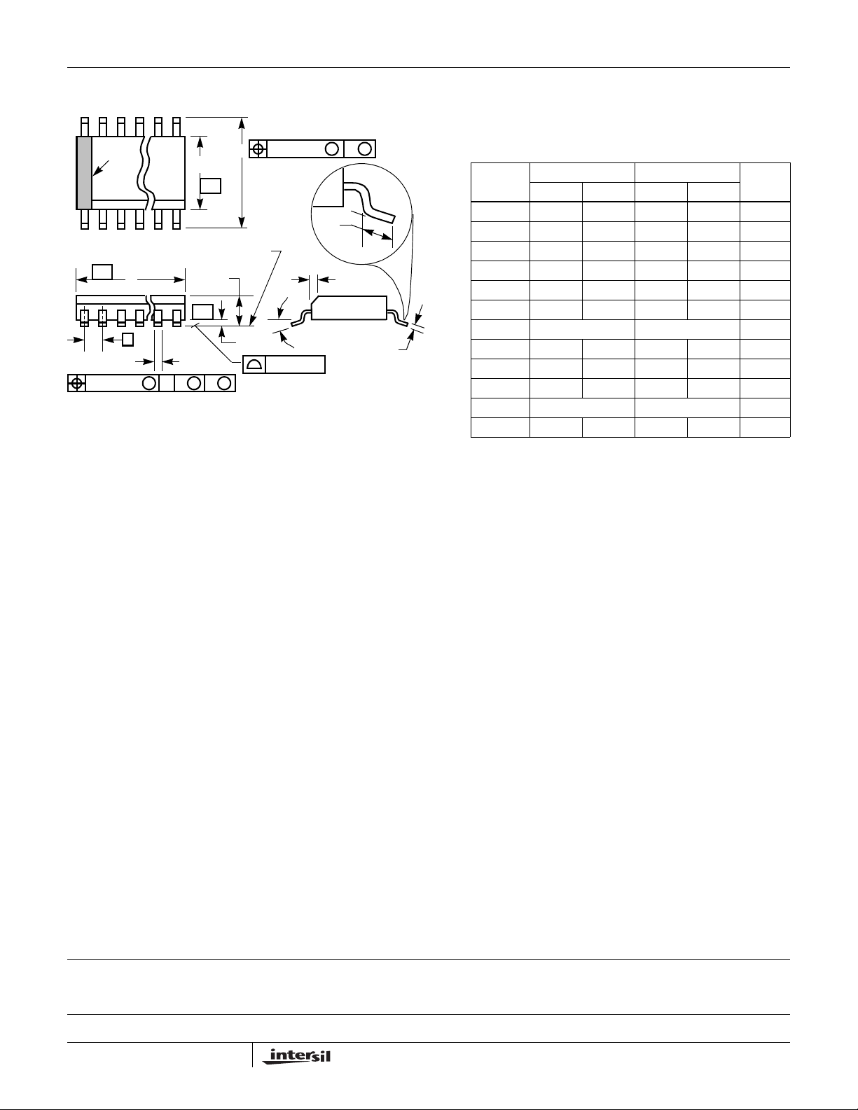
Small Outline Plastic Packages (SOIC)
www.BDTIC.com/Intersil
ISL5571A
N
INDEX
AREA
123
-AD
e
B
0.25(0.010) C AM BS
NOTES:
1. Symbols are defined in the “MO Series Symbol List” in Section 2.2 of
Publication Number 95.
2. Dimensioning and tolerancing per ANSI Y14.5M-1982.
3. Dimension “D” does not include mold flash, protrusions or gate burrs.
Mold flash, protrusion and gate burrs shall not exceed 0.15mm (0.006
inch) per side.
4. Dimension “E” does not include interlead flash or protrusions. Interlead
flash and protrusions shall not exceed 0.25mm (0.010 inch) per side.
5. The chamfer on the body is optional. If it is not present, a visual index
feature must be located within the crosshatched area.
6. “L” is the length of terminal for soldering to a substrate.
7. “N” is the number of terminal positions.
8. Terminal numbers are shown for reference only.
9. The lead width “B”, as measured 0.36mm (0.014 inch) or greater above
the seating plane, shall not exceed a maximum value of 0.61mm (0.024
inch)
10. Controlling dimension: MILLIMETER. Converted inch dimensions are
not necessarily exact.
E
-B-
SEATING PLANE
A
-C-
M
0.25(0.010) BM M
H
α
µ
A1
0.10(0.004)
L
h x 45
o
C
M16.3 (JEDEC MS-013-AA ISSUE C)
16 LEAD WIDE BODY SMALL OUTLINE PLASTIC PACKAGE
INCHES MILLIMETERS
SYMBOL
A 0.0926 0.1043 2.35 2.65 -
A1 0.0040 0.0118 0.10 0.30 -
B 0.013 0.0200 0.33 0.51 9
C 0.0091 0.0125 0.23 0.32 D 0.3977 0.4133 10.10 10.50 3
E 0.2914 0.2992 7.40 7.60 4
e 0.050 BSC 1.27 BSC -
H 0.394 0.419 10.00 10.65 -
h 0.010 0.029 0.25 0.75 5
L 0.016 0.050 0.40 1.27 6
N16 167
o
α
0
o
8
o
0
o
8
Rev. 0 12/93
NOTESMIN MAX MIN MAX
-
All Intersil U.S. products are manufactured, assembled and tested utilizing ISO9000 quality systems.
Intersil Corporation’s quality certifications can be viewed at www.intersil.com/design/quality
Intersil products are sold by description only. Intersil Corporation reserves the right to make changes in circuit design, software and/or specifications at any time without
notice. Accordingly, the reader is ca utioned to verify that data she ets are current before pl acing orders. Information fur nished by Intersil is believed to be accurate and
reliable. However, no responsibility is assumed by Intersil or its subsidiaries for its use; nor for any infringements of patents or other rights of third parties which may result
from its use. No license is granted by implication or othe rwise under any patent or patent rights of Intersil or its subsidia ries.
For information regarding Intersil Corporation and its products, see www.intersil.com
12
 Loading...