

Page 1

1
®
AN1270.0
ISL55141, ISL55142, ISL55143
Evaluation Board User’s Manual
Before Getting Started
This document supplements the ISL55141, ISL55142,
ISL55143 specification FN6230. Evaluation board users
should review that document to obtain information on the
part’s basic functionality and power requirements. A most
important note is before powering up the board, review
the Power-up Sequence in that specification. There are
many DC sources utilized, therefore a user may
inadvertently mis-apply the power sources causing damage
to the part.
T ake time to review the ISL55141, ISL55142, ISL55143 Data
Sheet (FN6230) and become familiar with the part’s basic
functions and power options. Note also that FN6230 super
cedes this document with respect to updates and
modifications. Always refer to that document if discrepancies
occur.
No voltage should be greater than VCC or less than VEE.
Also, VOH must be greater than VOL. Since there are so
many variations of use, each evaluation board provides
three jumpers relating to basic power strapping.
All ISL55141, ISL55142, ISL55143 boards are designed
essentially in the same fashion. This document provides the
user with the information regarding the evaluation board
design, circuitry layout and jumper options.
Jumper Options - VEE, VOL and GND
First, VEE can be negative with respect to ground for
receiving negative input ranges on the VINPs (comparator
Inputs). The comparator outputs QA, QB toggle between
VOH and VOL. VOL could also be a negative voltage,
although this is usually not the case. VOL should never be
more negative than VEE.
For single supply operations, the user may wish to connect
VEE to ground and VOL as well. Therefore, on each
evaluation board there are positions for three jumpers (JP01,
JP02, JP03).
The user should make note that the ISL55141, ISL55142,
ISL55143 all operate with VEE as the negative reference.
There are no actual ground connection to the comparators
unless VEE itself is connected to ground.
Before beginning the evaluation, the user should determine
the desired relationship between GND, VEE and VOL.
JP01 Connects VOL to VEE
Both VEE and VOL voltage busses are negative with respect
to ground. Comparator receives negative inputs and
translates the QA/QB outputs with a negative low voltage.
JP02 Connects VOL to GND
VOL low is connected to ground, VEE is negative with
respect to ground. Comparator inputs operate below ground
but QA/QB level translation in reference to ground.
JP03 Connects VEE to GND
Both VOL and VEE are referenced to ground. There are no
negative voltage requirements with respect to Comparator
Inputs or level translation on the QA/QB Outputs
FIGURE 1. THERE ARE NO GROUND PINS ON THESE
COMPARATORS. VEE ALWAYS PROVIDES THE
MOST NEGATIVE POWER CONNECTION.
PD
14
CVB
12
VINP
11
CVA
10
VCC
9
VEE
8
VEE
1
QA
4
QB
5
VOL
6
VOH
7
ISL55141_TSSOP
FIGURE 2. THREE JUMPERS ARE A V AILABLE T O SET USER
POWER STRAPPING OPTIONS.
VOL - Banana Jack
C1
+4.7µF
C2
0.1µF
DIF--
DIF+
TP03-VOH_VOL
VOH - Banana Jack
1
2
JP01
VOL = VEE
JP02
VOL = GND
JP03
VEE = GND
VOL
VEE
GND
VOH
VOL
GND - Banana Jack VEE - Banana Jack
C4
+4.7µF
C3
0.1µF
VCC
DIF--
DIF+
TP04_VCC_VEE
GND
VOL
VEE
VCC - Banana Jack
1
2
1
2
Application Note September 27, 2006
CAUTION: These devices are sensitive to electrostatic discharge; follow proper IC Handling Procedures.
1-888-INTERSIL or 1-888-468-3774
| Intersil (and design) is a registered trademark of Intersil Americas Inc.
Copyright Intersil Americas Inc. 2006. All Rights Reserved
All other trademarks mentioned are the property of their respective owners.
Page 2
2
AN1270.0
September 27, 2006
Scope Probe Connections
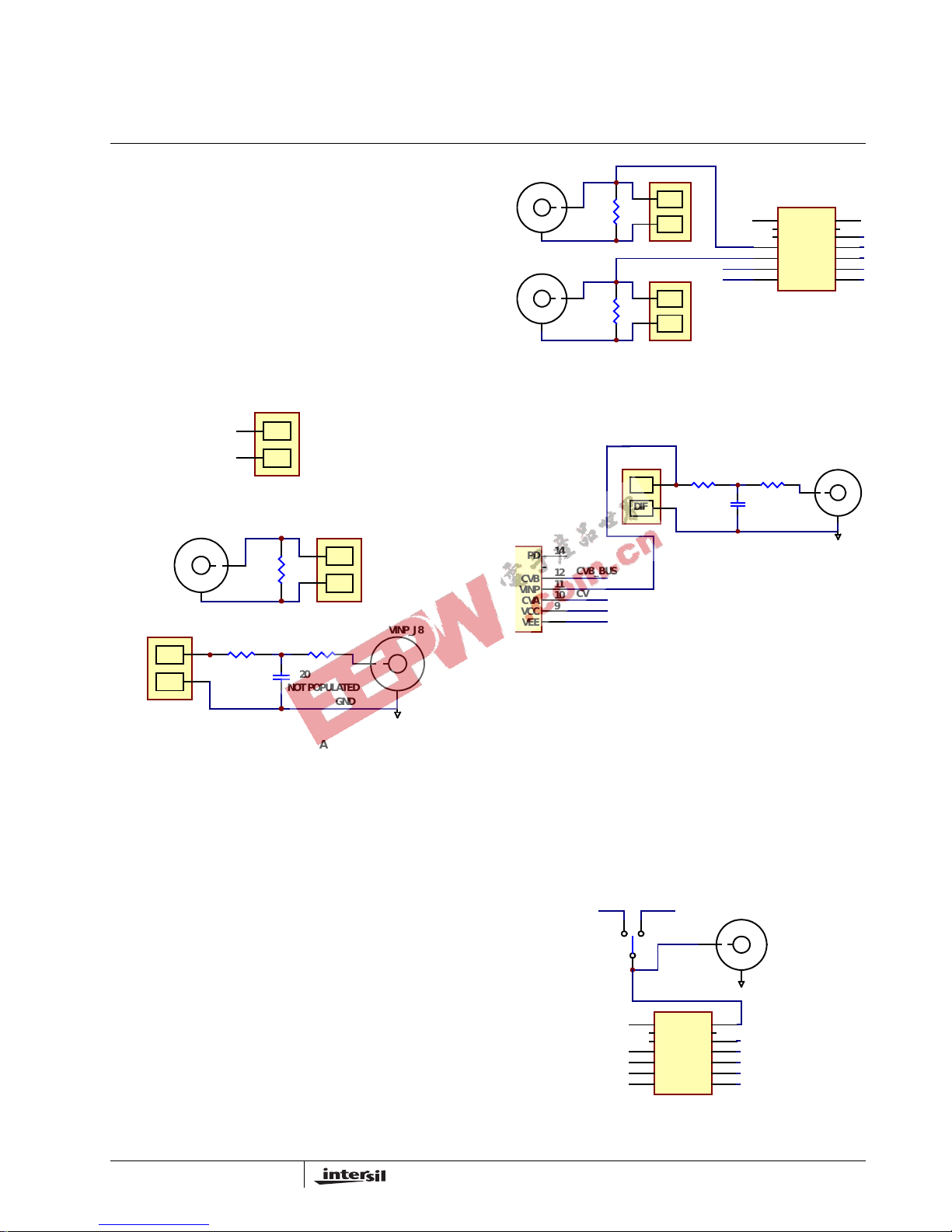
Another topic to cover before getting started is the evaluation
board physical connections for waveform observations. On
each schematic version you will see a component with pins
designated as DIF+ and DIF-. This is not an active
component but a dual pin header physically design to
accommodate connection of active differential probes. This
will minimize ground lead inductance and capacitive loading
while make waveform observations. However, the user must
also be mindful of max voltage limitations when using these
types of probes. The ISL5514x comparators cover a large
voltage range, so double check the probe’s specifications.
Scope probe test points (TP) are positioned across all
inputs, outputs and VCC and VEE.
BNC Connections
This series of evaluation boards also provides BNC
connections for input and output signals. A key point to
remember is the ISL55141, ISL55142, ISL55143 comparator
outputs (QA/QB) operate with the VOH voltage as a High
and VOL voltage as a Low. QA/QB BNC’s, which are
connected to the outputs, have the shield connected to the
VOL voltage bus. Keep this in mind when making BNC
connections to avoid connecting the GND shield of the BNC
inputs to the VOL shield of the BNC outputs.
Also note that the comparator outputs have 50Ω
terminations that you may need to remove for your
application.
Power-Down Feature
All boards provide the same capability for testing the
power-down feature. A SPDT- center OFF switch is provided
for manual testing of the feature. In one position the PD input
is connected to VCC (Power-down enabled). In the other
position the PD Input is connected to VEE (power-down
disabled).
FIGURE 3. DUAL1” SPACED PINS ARE PLACED ON THE
EVALUATION BOARDS FOR DIFFERENTIAL
PROBE CONNECTIONS
R1
50Ω
DIF--
DIF+
TP01-QA_VOLQA_J3 QA0
VOL
R14
0Ω
R18
0Ω
R20
NOT POPULATED
DIF--
DIF+
TP07-VINP VINP_J8
GND
GND
DIF--
DIF+
SCOPE PROBE CONNECTIONS
FIGURE 4. BNC CONNECTIONS ON THE QA/QB
COMPARATOR OUTPUTS HAVE THE SHIELD
CONNECTED TO THE VOL BUS. NOTE: YOU MA Y
WISH TO REMOVE THE 50Ω TERMINATIONS.
R1
50Ω
R2
50Ω
DIF--
DIF+
TP01-QA_VOL
DIF--
DIF+
TP02-QB_VOL
QA_J3
QB_J4
QA0
QB0
QB0
QA0
VOH
VOL
VOL
VOL
PD
14
CVB
12
VINP
11
CVA
10
VCC
9
VEE
8
VEE
1
QA
4
QB
5
VOL
6
VOH
7
ISL55141_TSSOP
FIGURE 5. BNC CONNECTIONS ON THE HIGH SPEED VINP
PINS HAVE THE SHIELD CONNECTED TO GND.
NOTE: TWO SMD SERIES POSITIONS PLUS ONE
POSITION TO GROUND ARE AVAILABLE FOR
USER SPECIFIC CIRCUITRY.
VCC
CVB_BUS
CVA_BUS
VINP
VEE
_TSSOP
R14
0Ω
R18
0Ω
R20
NOT POPULATED
DIF--
DIF+
TP07-VINP
VINP_J8
GND
VINP
GND
PD
14
CVB
12
VINP
11
CVA
10
VCC
9
VEE
8
FIGURE 6. ALL ISL5514X EVALUA TION BOARDS HA VE THE
SAME POWER-DOWN CIRCUITRY.
S1 - POWER-DOWN CONTROL
SPDT - CENTER OFF
VDD
GND
PD - BN_J5
VEE
PD
PD
14
CVB
12
VINP
11
CVA
10
VCC
9
VEE
8
VEE
1
QA
4
QB
5
VOL
6
VOH
7
ISL55141_TSSOP
Application Note 1270
Page 3

3
AN1270.0
September 27, 2006
Finally the center off position provides a means of
connecting a repetitive signal source to the PD input. This is
so the user can observe power-down enable/disable timing.
An important note to remember when using the PD - BNC:
1. Place the switch in center-off position.
2. The PD input is referenced to VCC/VEE. The low
amplitude of the PD input must match the VEE voltage.
The high amplitude must be close to VCC.
Comparator Threshold Rails
Each comparator has two thresholds. CVA/CVB. The data
sheet explains the operation of these analog inputs.
However, it should be mentioned that while the ISL55142
(Dual) and ISL55143 (QUAD) comparators have separate
threshold inputs for each comparator, the evaluation boards
have all CVA inputs tied to single CVA_BUS. Accordingly, all
CVB inputs are tied to a single CVB_BUS.
Initial Power-Up
Please refer to the device specification for power-up
sequencing and current requirements. Also note that the
frequency of operation and number of comparators will
determine the current needed. There are graphs in the
specification regarding current characteristics.
When first powering up the device, set all power bus inputs
to minimum current levels needed for quiescent operation.
Check the device out statically with DC inputs on the VINP
pins and observe that the QA/QB outputs toggle when the
VINP voltage crosses the CVA and CVB thresholds.
Once static observations check out, you can then increase
power current limits for VCC/VEE and VOH/VOL and apply
higher frequency inputs to the VINP pins.
Layout Information
All evaluation boards have complete silk-screen information
regarding test points, jumpers and component placements.
The silk-screen on the board you receive will provide
up-to-date layout information.
Schematic Information
Schematics are drawn with physical location in mind. Any
changes in electrical circuitry will be updated in this
document as needed.
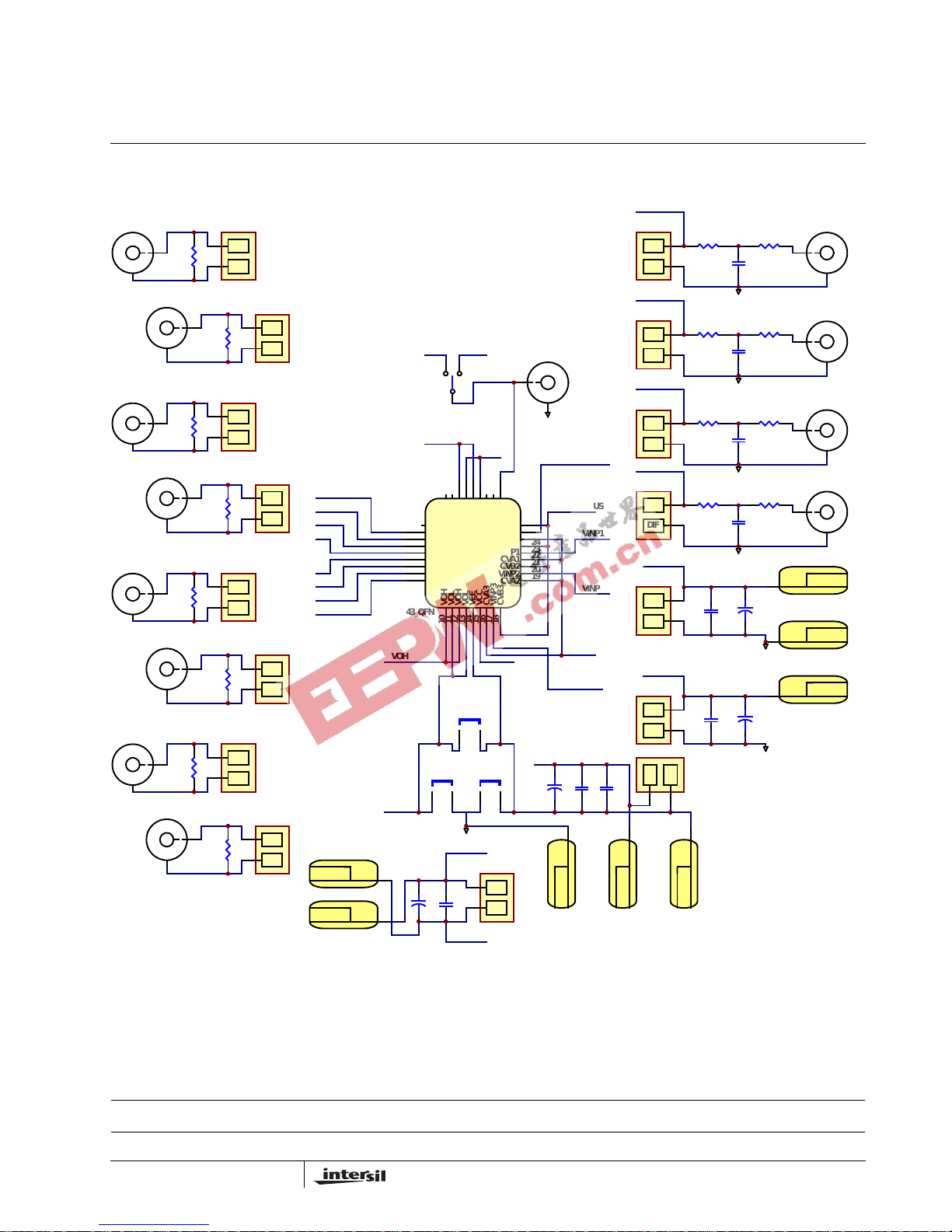
Included in the following pages are three schematics.
ISL55141 single comparator device, ISL55142 dual
comparator and ISL55143 quad comparator device. The
Evaluation boards are laid out for the TSSOP packages for
the ISL55141 and ISL55142, while the ISL55143 is the QFN
package. Please refer to the device specification for part
numbers/options for these and other package ordering.
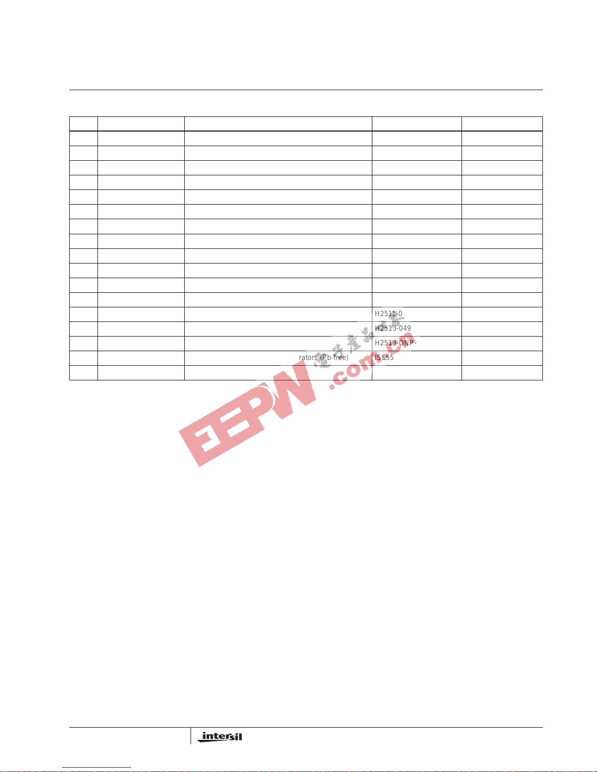
Bill of Material
A bill of material of the ISL55142 evaluation board is
included on page 6. It provides sources for special
components such as the BNC connectors and banana jacks.
All other parts are QPL standard passive components. Refer
to device specification (FN6230) when ordering
replacements for actual ISL55141, ISL55142 or ISL55143
devices.
FIGURE 7. ISL55142 AND ISL55143 COMPARA TOR
THRESHOLD CVA/CVB INPUTS ARE TIED
TOGETHER TO EITHER THE CVA_BUS OR
CVB_BUS.
QA0
2
QB0
3
QA1
4
VINP2
20
VINP0
26
CVB0
27
VOL
11
VOH12VOL13VEE
14
VCC
34
QB1
5
CVA2
19
VCC
15
VEE
33
QA2
6
QB2
7
QA3
8
QB3
9
CVA3
16
VINP317CVB3
18
VOH
10
CVA1
22
VINP1
23
CVA0
25
CVB1
24
CVB2
21
VCC
32
VEE
31PD28
ISL55143_QFN
CVB_BUS
CVA_BUS
Application Note 1270
Page 4
4
AN1270.0
September 27, 2006
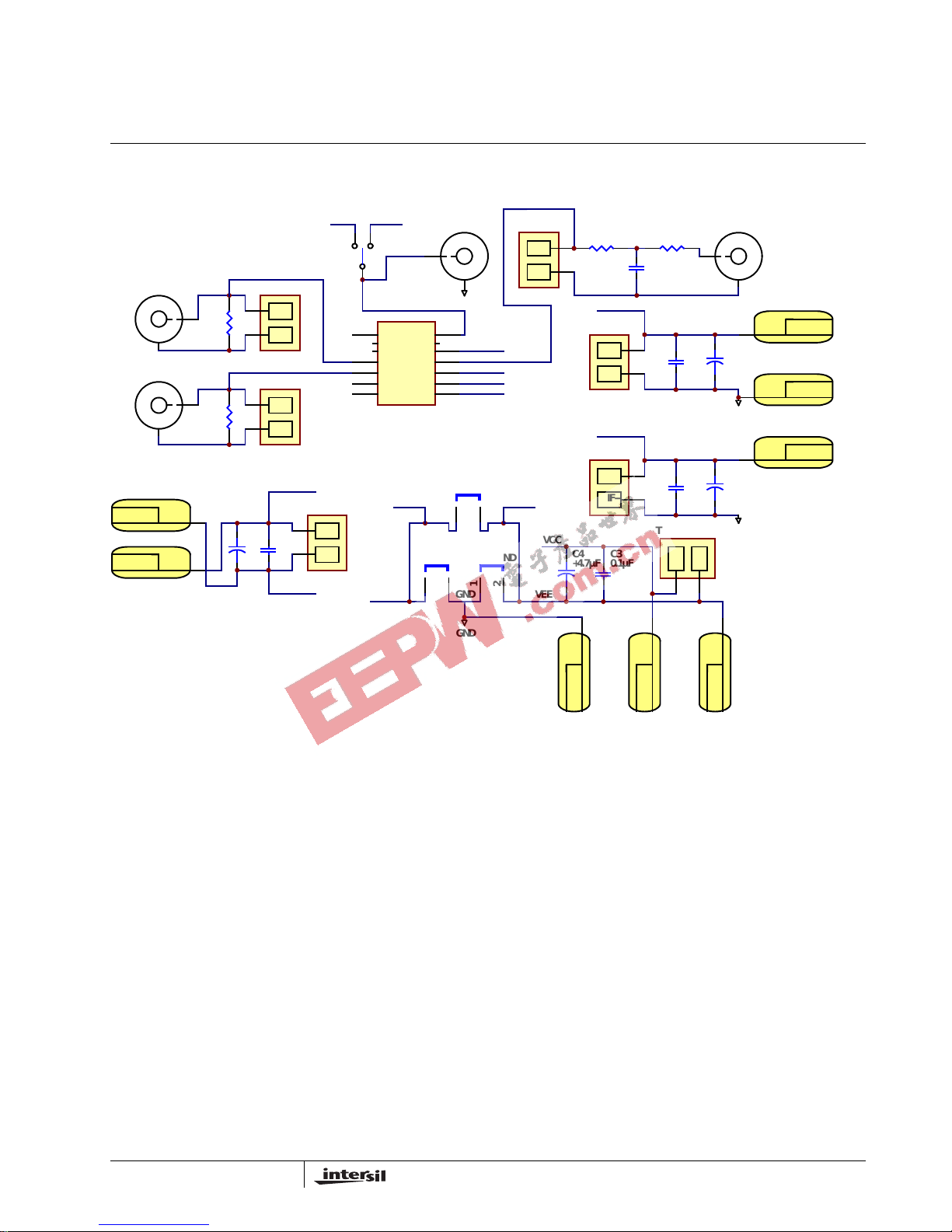
ISL55142IVZ Evaluation Board Schematic
FIGURE 8. ISL55141IVZ TSSOP SINGLE COMPARATOR EVALUATION BOARD SCHEMATIC
S1 - POWER-DOWN CONTROL
SPDT - CENTER OFF
C7
+4.7µF
R1
50Ω
R2
50
Ω
J9-CVB - Banana Jack
C5
0.1µF
VDD
CVB_BUS
GND
GND
DIF--
DIF+
TP01-QA_VOL
DIF--
DIF+
TP02-QB_VOL
DIF--
DIF+
TP06_CVB
QA_J3
QB_J4
PD - BN_J5
C8
+4.7µF
J10-GND - Banana Jack
J11-CVA - Banana Jack
C6
0.1µF
CVA_BUS
GND
DIF--
DIF+
TP05_CVA
VOL - Banana Jack
C1
+4.7µFC20.1µF
DIF--
DIF+
TP03-VOH_VOL
VOH - Banana Jack
QB0
QA0
1
2
JP01
VOL = VEE
1
2
JP02
VOL = GND
1
2
JP03
VEE = GND
VOL VEEGND
VCC
VOH
VOL
GND - Banana Jack VEE - Banana Jack
C4
+4.7µFC30.1µF
VCC
DIF--
DIF+
TP04_VCC_VEE
GND
GND
GND
CVB_BUS
CVA_BUS
CVB_BUS
CVA_BUS
VEE
VINP
VOL
VOL
VEE
PD
VOL
VEE
R14
0Ω
R18
0Ω
R20
NOT POPULATED
DIF--
DIF+
TP07-VINP
VINP_J8
GND
VINP
VCC - Banana Jack
PD
14
CVB
12
VINP
11
CVA
10
VCC
9
VEE
8
VEE
1
QA
4
QB
5
VOL
6
VOH
7
ISL55141_TSSOP
Application Note 1270
Page 5
5
AN1270.0
September 27, 2006
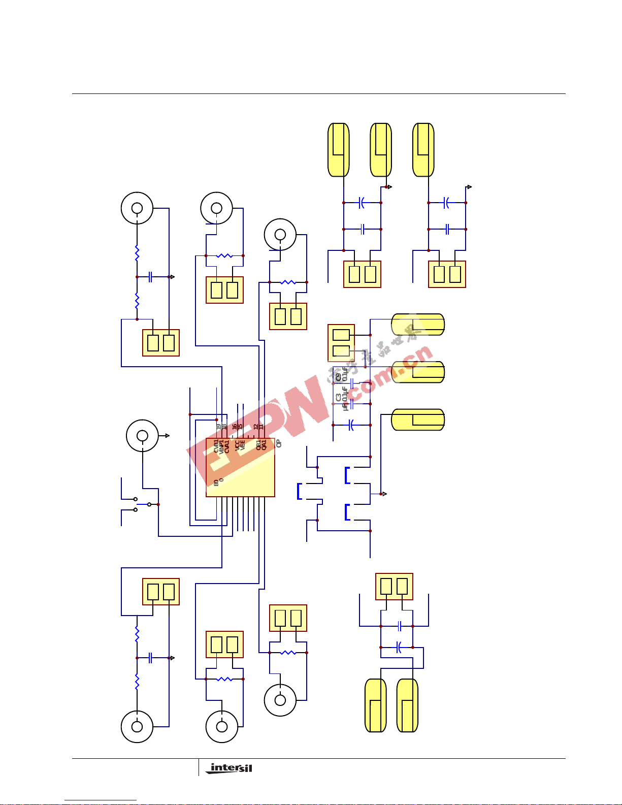
ISL55142IVZ Evaluation Board Schematic
S1 - POWER-DOWN CONTROL
SPDT - CENTER OFF
+
C7
4.7µF
R1
50Ω
R2
50Ω
J9-CVB - Banana Jack
C5
0.1µF
VDD
CVB_BUS
GND
GND
DIF--
DIF+
TP01-QA0_VOL
DIF--
DIF+
TP02-QB0_VOL
DIF--
DIF+
TP06_CVB
QA0_J3
QB0_J4
PD - BN_J5
R7
50Ω
DIF--
DIF+
TP10-QB1_VOL
QB1_J13
C8
+4.7µF
J10-GND - Banana Jack
J11-CVA - Banana Jack
C6
0.1µF
CVA_BUS
GND
DIF--
DIF+
TP05_CVA
VOL - Banana Jack
C1
+4.7µF
C2
0.1µF
DIF--
DIF+
TP03-VOH_VOL
VOH - Banana Jack
QA0
QB0 QA1
QB1
QB1
QB0
QA0
1
2
JP01
VOL = VEE
1
2
JP02
VOL = GND
1
2
JP03
VEE = GND
VOL
VEEGND
VOH
VCC
VCCVEE
VOH
VOL
GND - Banana Jack VCC - Banana Jack VEE - Banana Jack
C4
+4.7µF
C3
0.1µF
VCC
DIF--
DIF+
TP04_VCC_VEE
GND
C9
0.1µF
R10
0Ω
R8
0Ω
R9
NOT POPULATED
GND
DIF--
DIF+
TP07-VINP1
VINP1_J14
GND
R14
0Ω
R18
0Ω
R20
NOT POPULATED
GND
DIF--
DIF+
TP10-VINP0
VINP0_J8
GND
GND
GND
CVB_BUS
CVA_BUS
VINP1
VINP1
VINP0
CVB_BUS
CVA_BUS
VEE
CVB01VINP02CVA03VEE
5
CVA1
18
CVB1
20
VINP1
19
.
PD4VCC6VOH7VOL8QA09QB0
10
VCC
16
VEE15QB112QA1
11
ISL55142IVZ_TSSOP
R6
50Ω
DIF--
DIF+
TP09-QA1_VOL
QA1_J12
QA1
VINP0
VOL
VOLVOL
VOL VOL
VEE
PD
VOL
VEE
FIGURE 9. ISL55142IVZ TSSOP DUAL COMPARATOR EVALUATION BOARD
Application Note 1270
Page 6
6
AN1270.0
September 27, 2006
ISL5514x Bill of Materials
QTY REF DES DESCRIPTION PART NUMBER MANUFACTURER
7 J3-J5, J8, J12-J14 50Ω PCB mount receptacle 31-5329-52RFX AMPHENOL
2 J7, J10 Right angle PCB mount insulated socket - single (black) 571-0100 DELTRON
1 J1 Right angle PCB mount insulated socket - single (blue) 571-0200 DELTRON
1 J20 Right angle PCB mount insulated socket - single (brown) 571-0300 DELTRON
1 J2 Right angle PCB mount insulated socket - single (green) 571-0400 DELTRON
1 J6 Right angle PCB mount insulated socket - single (red) 571-0500 DELTRON
1 J9 Right angle PCB mount insulated socket - single (white) 571-0600 DELTRON
1 J11 Right angle PCB mount insulated socket - single (yellow) 571-0700 DELTRON
2 C5, C6 Multilayer cap C1608X7R1H104K TDK
1 S1 Sealed subminiature toggle switch ET03SD1CBE ITT CANNON-C&K
3 C2, C3, C9 Multilayer cap H1045-00104-25V10 GENERIC
4 C1, C4, C7, C8 Multilayer cap H1065-004R7-50VR25 GENERIC
4 R3, R5, R8, R10 Thick film chip resistor H2511-00R00-1/16W1 GENERIC
4 R1, R2, R6, R7 Thick film chip resistor H2513-049R9-1/8W1 GENERIC
2 R4, R9 Thick film chip resistor (do not populate) H2513-DNP-DNP-1 GENERIC
1 U1 High-speed CMOS window comparators (Pb-free) ISL55142ARZ INTERSIL
13 JP01-JP03, TP01-TP010 Two-pin jumper JUMPER2_100 GENERIC
Application Note 1270
Page 7
7
Intersil Corporation reserves the right to make changes in circuit design, software and/or specifications at any time without notice. Accordingly, the reader is cautioned to
verify that the Application Note or Technical Brief is curren t befor e procee di ng.
For information regarding Intersil Corporation and its products, see www.intersil.com
AN1270.0
September 27, 2006
ISL55143IRZ Evaluation Board Schematic
FIGURE 10. ISL55143IRZ QFN QUAD COMPARATOR EVALUATION BOARD
S1 - POWER-DOWN CONTROL
SPDT - CENTER OFF
C7
+4.7µF
R5
0Ω
R3
0Ω
R1
50Ω
R2
50
Ω
J9-CVB - Banana Jack
C5
0.1µF
VDD
R4
NOT POPULATED
GND
CVB_BUS
GND
GND
DIF--
DIF+
TP01-QA0_VOL
DIF--
DIF+
TP02-QB0_VOL
DIF--
DIF+
TP10-VINP3
DIF--
DIF+
TP16_CVB
QA0_J3
QB0_J4
VINP3_J8
PD - BN_J5
QA0
2
QB0
3
QA1
4
VINP2
20
VINP0
26
CVB0
27
VOL11VOH12VOL13VEE
14
VCC
34
QB1
5
CVA2
19
VCC
15
VEE
33
QA2
6
QB2
7
QA3
8
QB3
9
CVA316VINP317CVB3
18
VOH
10
CVA1
22
VINP1
23
CVA0
25
CVB1
24
CVB2
21
VCC
32
VEE
31PD28
ISL55143_QFN
R12
50Ω
R16
50Ω
DIF--
DIF+
TP03-QA1_VOL
DIF--
DIF+
TP05-QB1_VOL
QA1_J18
QB1_J21
R11
50Ω
R15
50Ω
DIF--
DIF+
TP05-QA3_VOL
DIF--
DIF+
TP06-QB2_VOL
QA2_J17
QB2_J21
R6
50Ω
R7
50Ω
DIF--
DIF+
TP07-QA3_VOL
DIF--
DIF+
TP08-QB3_VOL
QA3_J12
QB3_J13
C8
+4.7µF
J10-GND - Banana Jack
J11-CVA - Banana Jack
C6
0.1µF
CVA_BUS
GND
DIF--
DIF+
TP15_CVA
VOL - Banana Jack
C1
+4.7µF
C2
0.1µF
DIF--
DIF+
TP03-VOH_VOL
VOH - Banana Jack
QA0
QB0
QA1
QB1
QA2
QB2
QA3
QB3
QB3
QA3
QB2
QA2
QB1
QA1
QB0
QA0
1
2
JP01
VOL = VEE
1
2
JP02
VOL = GND
1
2
JP03
VEE = GND
VOL
VEE
GND
VOH
VCC
VCC
VEE
VOH
VOL
GND - Banana Jack VEE - Banana Jack
C4
+4.7µFC30.1µF
VCC
DIF--
DIF+
TP01_VCC_VEE
GND
C9
0.1µF
GND
R6
0Ω
R4
0Ω
C9
NOT POPULATED
GND
DIF--
DIF+
TP10-VINP2 VINP2_J14
GND
R10
0Ω
R8
0Ω
R9
NOT POPULATED
GND
DIF--
DIF+
TP10-VINP1
VINP1_J15
GND
R14
0Ω
R18
0Ω
R20
NOT POPULATED
GND
DIF--
DIF+
TP10-VINP0 VINP0_J16
GND
GND
CVB_BUS
CVA_BUS
VINP0
VINP1
VINP2
VINP3
VINP0
VINP1
VINP2
VINP3
CVB_BUS
CVA_BUS
VEE
VCC - Banana Jack
GND
Application Note 1270
 Loading...