

Page 1
®
ISL55002
Data Sheet July 27, 2006
High Supply Voltage 200MHz Unity-Gain
Stable Operational Amplifier
The ISL55002 is a high speed, low power, low cost
monolithic operational amplifier. The ISL55002 is unity-gain
stable and features a 300V/µs slew rate and 200MHz
bandwidth while requiring only 8.5mA of supply current per
amplifier.
The power supply operating range of the ISL55002 is from
±15V down to ±2.5V. For single-supply operation, the
ISL55002 operates from 30V down to 5V.
The ISL55002 also features an extremely wide output
voltage swing of -12.75V/+13.4V with V
R
=1kΩ.
L
= ±15V and
S
At a gain of +1, the ISL55002 has a -3dB bandwidth of
200MHz with a phase margin of 55°. Because of its
conventional voltage-feedback topology, the ISL55002 allow
the use of reactive or non-linear elements in its feedback
network. This versatility combined with low cost and 140mA
of output-current drive makes the ISL55002 an ideal choice
for price-sensitive applications requiring low power and high
speed.
The ISL55002 is available in an 8 Ld SO package and is
specified for operation over the full -40°C to +85°C
temperature range.
Ordering Information
TAPE
PART
PART NUMBER
ISL55002IB 55002IB - 8 Ld SO MDP0027
ISL55002IB-T7 55002IB 7” 8 Ld SO MDP0027
ISL55002IB-T13 55002IB 13” 8 Ld SO MDP0027
ISL55002IBZ
(See Note)
ISL55002IBZ-T7
(See Note)
ISL55002IBZ-T13
(See Note)
NOTE: Intersil Pb-free plus anneal products employ special Pb-free
material sets; molding compounds/die attach materials and 100%
matte tin plate termination finish, which are RoHS compliant and
compatible with both SnPb and Pb-free soldering operations. Intersil
Pb-free products are MSL classified at Pb-free peak reflow
temperatures that meet or exceed the Pb-free requirements of
IPC/JEDEC J STD-020.
MARKING
55002IBZ - 8 Ld SO
55002IBZ 7” 8 Ld SO
55002IBZ 13” 8 Ld SO
&
REEL PACKAGE
(Pb-Free)
(Pb-Free)
(Pb-Free)
PKG.
DWG. #
MDP0027
MDP0027
MDP0027
FN7497.4
Features
• 200MHz -3dB bandwidth
• Unity-gain stable
• Low supply current: 8.5mA per amplifier
• Wide supply range: ±2.5V to ±15V dual-supply and 5V to
30V single-supply
• High slew rate: 300V/µs
• Fast settling: 75ns to 0.1% for a 10V step
• Wide output voltage swing: -12.75V/+13.4V with
= ±15V, RL=1kΩ
V
S
• Enhanced replacement for EL2244
• Pb-free plus anneal available (RoHS compliant)
Applications
• Video amplifiers
• Single-supply amplifiers
• Active filters/integrators
• High speed sample-and-hold
• High speed signal processing
• ADC/DAC buffers
• Pulse/RF amplifiers
• Pin diode receivers
• Log amplifiers
• Photo multiplier amplifiers
• Difference amplifiers
Pinout
ISL55002
(8 LD SO)
TOP VIEW
OUT
IN1-
IN1+
VS-
1
2
-+
3
4
8
VS+
OUT2
7
IN2-
6
-+
IN2+
5
1
CAUTION: These devices are sensitive to electrostatic discharge; follow proper IC Handling Procedures.
1-888-INTERSIL or 1-888-468-3774
| Intersil (and design) is a registered trademark of Intersil Americas Inc.
All other trademarks mentioned are the property of their respective owners.
Copyright Intersil Americas Inc. 2005-2006. All Rights Reserved
Page 2
ISL55002
Absolute Maximum Ratings (T
Supply Voltage (V
Input Voltage (V
Differential Input Voltage (dVIN). . . . . . . . . . . . . . . . . . . . . . . . .±10V
Continuous Output Current . . . . . . . . . . . . . . . . . . . . . . . . . . . 60mA
CAUTION: Stresses above those listed in “Absolute Maximum Ratings” may cause permanent damage to the device. This is a stress only rating and operation of the
device at these or any other conditions above those indicated in the operational sections of this specification is not implied.
IMPORTANT NOTE: All parameters having Min/Max specifications are guaranteed. Typical values are for information purposes only. Unless otherwise noted, all tests
are at the specified temperature and are pulsed tests, therefore: TJ = TC = T
). . . . . . . . . . . . . . . . . . . . . . . . . . ±16.5V or 33V
S
. . . . . . . . . . . . . . . . . . . . . . . . . . . . . . . . . . . .±V
IN)
DC Electrical Specifications V
= 25°C)
A
Power Dissipation (P
S
Operating Temperature Range (T
Operating Junction Temperature (T
) . . . . . . . . . . . . . . . . . . . . . . . . . See Curves
D
Storage Temperature (T
A
= ±15V, AV = +1, RL = 1kΩ, TA = 25°C, unless otherwise specified.
S
). . . . . . . . . . . . . .-40°C to +85°C
A
) . . . . . . . . . . . . . . . . . .+150°C
) . . . . . . . . . . . . . . . . . . .-65°C to +150°C
ST
J
PARAMETER DESCRIPTION CONDITION MIN TYP MAX UNIT
V
OS
TCV
OS
I
B
I
OS
TCI
OS
A
VOL
PSRR Power Supply Rejection Ratio V
CMRR Common-mode Rejection Ratio V
CMIR Common-mode Input Range V
V
OUT
Input Offset Voltage VS = ±15V 1.2 5 mV
Average Offset Voltage Drift (Note 1) -40°C to +85°C 17 µV/°C
Input Bias Current VS = ±15V 0.6 3.5 µA
Input Offset Current VS = ±15V 0.2 2 µA
Average Offset Current Drift (Note 1) 0.2 nA/°C
Open-loop Gain VS = ±15V, V
= ±5V to ±15V 75 100 dB
S
= ±10V, V
CM
= ±15V 13 V
S
= ±10V, RL = 1kΩ 12000 21000 V/V
OUT
= 0V 75 90 dB
OUT
Output Voltage Swing VO+, RL = 1kΩ 13.25 13.4 V
V
-, RL = 1kΩ -12.6 -12.75 V
O
V
+, RL = 150Ω 9.6 10.7 V
O
VO-, RL = 150Ω -8.3 -9.4 V
I
I
R
C
R
SC
S
IN
IN
OUT
Output Short Circuit Current 80 140 mA
Supply Current (per amplifier) VS = ±15V, no load 8.5 9.25 mA
Input Resistance 2.0 3.2 MΩ
Input Capacitance AV = +1 1 pF
Output Resistance AV = +1 50 mΩ
PSOR Power Supply Operating Range Dual supply ±2.25 ±15 V
Single supply 4.5 30 V
NOTE:
1. Measured from T
MIN
to T
MAX
.
AC Electrical Specifications V
= ±15V, AV = +1, RL = 1kΩ, TA = 25°C, unless otherwise specified.
S
PARAMETER DESCRIPTION CONDITION MIN TYP MAX UNIT
BW -3dB Bandwidth (V
GBWP Gain Bandwidth Product V
PM Phase Margin R
= 0.4VPP)V
OUT
= ±15V, AV = +1 200 MHz
S
= ±15V, AV = -1 50 MHz
V
S
V
= ±15V, AV = +2 50 MHz
S
V
= ±15V, AV = +5 17 MHz
S
= ±15V 70 MHz
S
= 1kΩ, CL = 5pF 55 °
L
SR Slew Rate (Note 1) 260 300 V/µs
2
FN7497.4
July 27, 2006
Page 3
ISL55002
AC Electrical Specifications V
PARAMETER DESCRIPTION CONDITION MIN TYP MAX UNIT
FPBW Full-power Bandwidth (Note 2) VS = ±15V 9.5 MHz
t
S
dG Differential Gain (Note 3) NTSC/PAL 0.01 %
dP Differential Phase NTSC/PAL 0.05 °
eN Input Noise Voltage 10kHz 12 nV/√Hz
iN Input Noise Current 10kHz 1.5 pA/√Hz
NOTES:
1. Slew rate is measured on rising edge.
2. For V
S
V
PEAK
3. Video performance measured at V
levels across a back-terminated 75Ω load. For other values or R
Settling to +0.1% (AV = +1) VS = ±15V, 10V step 75 ns
= ±15V , V
).
= 10VPP, for VS = ±5V , V
OUT
= ±15V, AV = +1, RL = 1kΩ, TA = 25°C, unless otherwise specified. (Continued)
S
= 5VPP. Full-power bandwidth is based on slew rate measurement using FPBW = SR/(2π *
OUT
= ±15V, AV = +2 with two times normal video level across RL = 150Ω. This corresponds to standard video
S
, see curves.
L
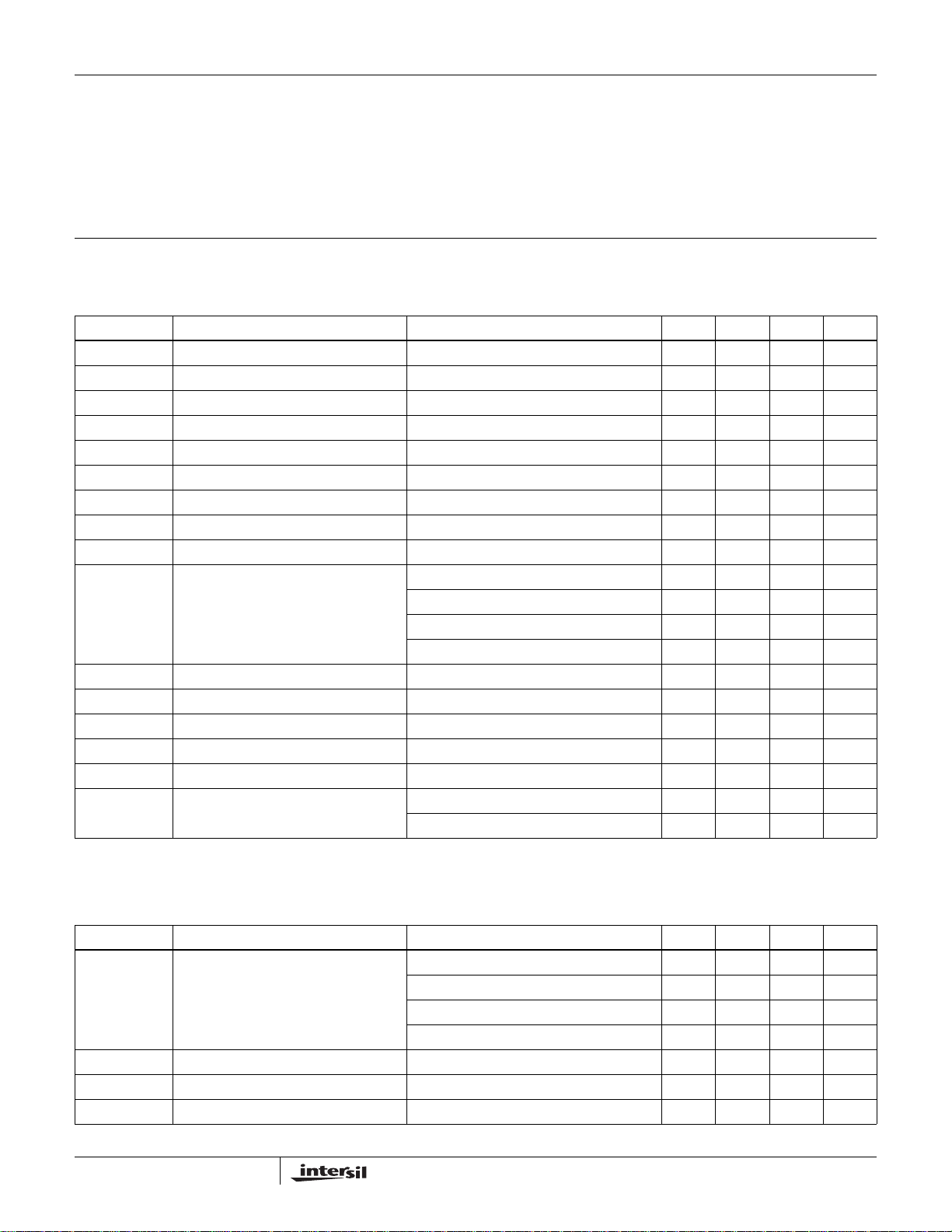
Typical Performance Curves
FIGURE 1. OPEN-LOOP GAIN vs FREQUENCY FIGURE 2. OPEN-LOOP PHASE vs FREQUENCY
FIGURE 3. GAIN vs FREQUENCY FOR VARIOUS NON-
INVERTING GAIN SETTINGS
FIGURE 4. GAIN vs FREQUENCY FOR VARIOUS INVERTING
GAIN SETTINGS
3
FN7497.4
July 27, 2006
Page 4
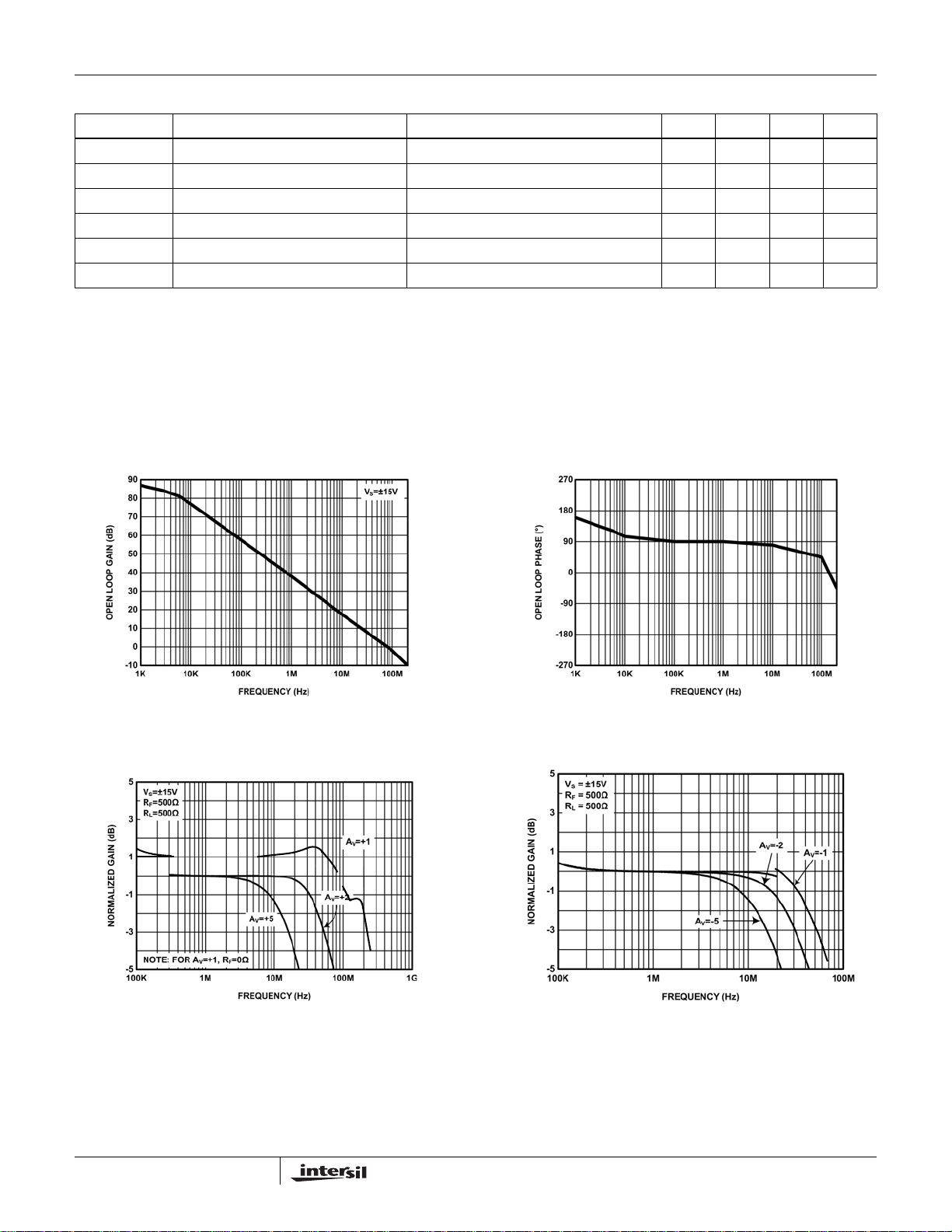
Typical Performance Curves (Continued)
ISL55002
FIGURE 5. PHASE vs FREQUENCY FOR VARIOUS NON-
INVERTING GAIN SETTINGS
100
RL=500Ω
80
60
40
20
GAIN BANDWIDTH PRODUCT [MHz]
0
06912153
SUPPLY VOLTAGES (±V)
FIGURE 6. PHASE vs FREQUENCY FOR VARIOUS
INVERTING GAIN SETTINGS
350
AV=+2
=500Ω
R
F
=500Ω
R
L
SLEW RATE (V/µs)
300
250
200
150
100
06912153
=5pF
C
L
SUPPL Y VOLTAGES (±V)
POSITIVE SLEW RATE
NEGATIVE SLEW RATE
FIGURE 7. GAIN BANDWIDTH PRODUCT vs SUPPLY FIGURE 8. SLEW RATE vs SUPPLY
FIGURE 9. GAIN vs FREQUENCY FOR VARIOUS R
(A
= +1)
V
4
LOAD
FIGURE 10. GAIN vs FREQUENCY FOR VARIOUS R
(A
= +2)
V
LOAD
FN7497.4
July 27, 2006
Page 5

Typical Performance Curves (Continued)
ISL55002
5
VS = ±15V
4
A
= +2
V
= 500Ω
R
F
3
= 500Ω
R
L
2
1
0
-1
-2
NORMALIZED GAIN (dB)
-3
-4
-5
100k 1M 10M 100M 1G
CL= 68pF
CL= 39pF
CL= 39pF
FREQUENCY (Hz)
CL= 100pF
CL= 22pF
FIGURE 11. GAIN vs FREQUENCY FOR VARIOUS C
(A
= +1)
V
5
VS = ±15V
4
AV = +1
= 500Ω
R
L
3
C
= 5pF
L
2
1
0
-1
-2
NORMALIZED GAIN (dB)
-3
-4
-5
100k 1M 10M 100M 1G
RF=100Ω
RF=0Ω
FREQUENCY (Hz)
RF=500Ω
RF=250Ω
FIGURE 13. GAIN vs FREQUENCY FOR VARIOUS R
(A
= +1)
V
4
VS = ±15V
3
= 500Ω
R
F
R
= 500Ω
L
2
C
= 5pF
L
= +2
A
1
V
0
-1
-2
-3
NORMALIZED GAIN (dB)
-4
-5
-6
100k 1M 10M 100M 1G
CIN = 10pF
CIN = 2.2pF
CIN = 0pF
FREQUENCY (Hz)
CIN = 6.8pF
CIN = 4.7pF
LOAD
FEEDBACK
FIGURE 15. GAIN vs FREQUENCY FOR VARIOUS INVERTING
INPUT CAPACITANCE (C
)
IN
FIGURE 12. GAIN vs FREQUENCY FOR VARIOUS C
(A
= +2)
V
5
VS = ±15V
4
A
= +2
V
= 500Ω
R
L
3
= 5pF
C
L
2
1
0
-1
-2
-3
NORMALIZED GAIN (dB)
-4
-5
100k 1M 10M 100M
FREQUENCY (Hz)
FIGURE 14. GAIN vs FREQUENCY FOR VARIOUS R
(A
= +2)
V
5
AV = +1
4
= 0Ω
R
F
R
= 500Ω
L
3
= 5pF
C
L
2
1
0
-1
-2
NORMALIZED GAIN (dB)
-3
-4
-5
100k 1M 10M 100M 1G
RF=100Ω
RF=250Ω
RF=500Ω
RF=1kΩ
VS = ±2.5V
VS = ± 5V
VS = ± 10V
VS = ± 15V
FREQUENCY (Hz)
LOAD
FEEDBACK
FIGURE 16. GAIN vs FREQUENCY FOR VARIOUS SUPPLY
SETTINGS
5
FN7497.4
July 27, 2006
Page 6

ISL55002
Typical Performance Curves (Continued)
FIGURE 17. COMMON-MODE REJECTION RATIO (CMRR) FIGURE 18. POWER SUPPLY REJECTION RATIO (PSRR)
-20
VS=±15V
=+1
A
-30
V
R
=0Ω
F
=500Ω
R
-40
L
=5pF
C
L
=2V
V
-50
OUT
P-P
-60
-70
-80
-90
HARMONIC DISTORTION (dBc)
-100
500K 1M 10M 40M
FREQUENCY (Hz)
THD
2ND HD
3RD HD
FIGURE 19. HARMONIC DISTORTION vs FREQ UENCY
(A
= +1)
V
FIGURE 21. OUTPUT SWING vs FREQUENCY FOR VARIOUS
GAIN SETTINGS
FIGURE 20. HARMONIC DISTORTION vs OUTPUT VOLTAGE
(AV = +2)
25
OUTPUT VOLTAGE SWING [Vp-p]
RL=500Ω
C
L
20
15
10
5
0
06912153
=5pF
SUPPLY VOLTAGES (±V)
Av=+1
R
Av=+2
=500Ω
F
FIGURE 22. OUTPUT SWING vs SUPPLY VOLTAGE FOR
VARIOUS GAIN SETTINGS
6
FN7497.4
July 27, 2006
Page 7

Typical Performance Curves (Continued)
ISL55002
20% to 80%
20% to 80%
80% to 20%
80% to 20%
FIGURE 23. LARGE SIGNAL RISE AND FALL TIMES FIGURE 24. SMALL SIGNAL RISE AND FALL TIMES
JEDEC JESD51-3 LOW EFFECTIVE THERMAL
25
20
15
10
AV=+1
R
TOTAL SUPPLY CURRENT (mA)
5
0
06912153
SUPPLY VOLTAGES (±V)
R
C
=0Ω
F
=500Ω
L
=5pF
L
FIGURE 25. SUPPLY CURRENT vs SUPPLY VOLTAGE
FIGURE 26. PACKAGE POWER DISSIP A TION vs AMBIENT
CONDUCTIVITY TEST BOARD
1.2
1
0.8
781mW
0.6
0.4
POWER DISSIPATION (W)
0.2
0
0 255075100 150
SO8
θJA=160°C/W
12585
AMBIENT TEMPERATURE (°C)
TEMPERATURE
JEDEC JESD51-7 HIGH EFFECTIVE THERMAL
CONDUCTIVITY TEST BOARD
1.8
1.6
1.4
1.2
1.136W
1
0.8
0.6
0.4
POWER DISSIPATION (W)
0.2
0
0 25 50 75 100 150
SO8
θJA=110°C/W
12585
AMBIENT TEMPERATURE (°C)
FIGURE 27. PACKAGE POWER DISSIPATION vs AMBIENT TEMPERATURE
7
FN7497.4
July 27, 2006
Page 8

ISL55002
Product Description
The ISL55002 is a wide bandwidth, low power, and low offset
voltage feedback operational amplifier. This device is
internally compensated for closed loop gain of +1 or greater.
Connected in voltage follower mode and driving a 500Ω
load, the -3dB bandwidth is around a 200MHz. Driving a
150Ω load and a gain of 2, the bandwidth is about 90MHz
while maintaining a 300V/µs slew rate.
The ISL55002 is designed to operate with supply voltage
from +15V to -15V. That means for single supply application,
the supply voltage is from 0V to 30V. For split supplies
application, the supply voltage is from ±15V. The amplifier
has an input common-mode voltage range from 1.5V above
the negative supply (V
supply (V
+ pin). If the input signal is outside the above
S
specified range, it will cause the output signal to be distorted.
The outputs of the ISL55002 can swing from -12.75V to
+13.4V for V
= ±15V. As the load resistance becomes
S
lower, the output swing is lower.
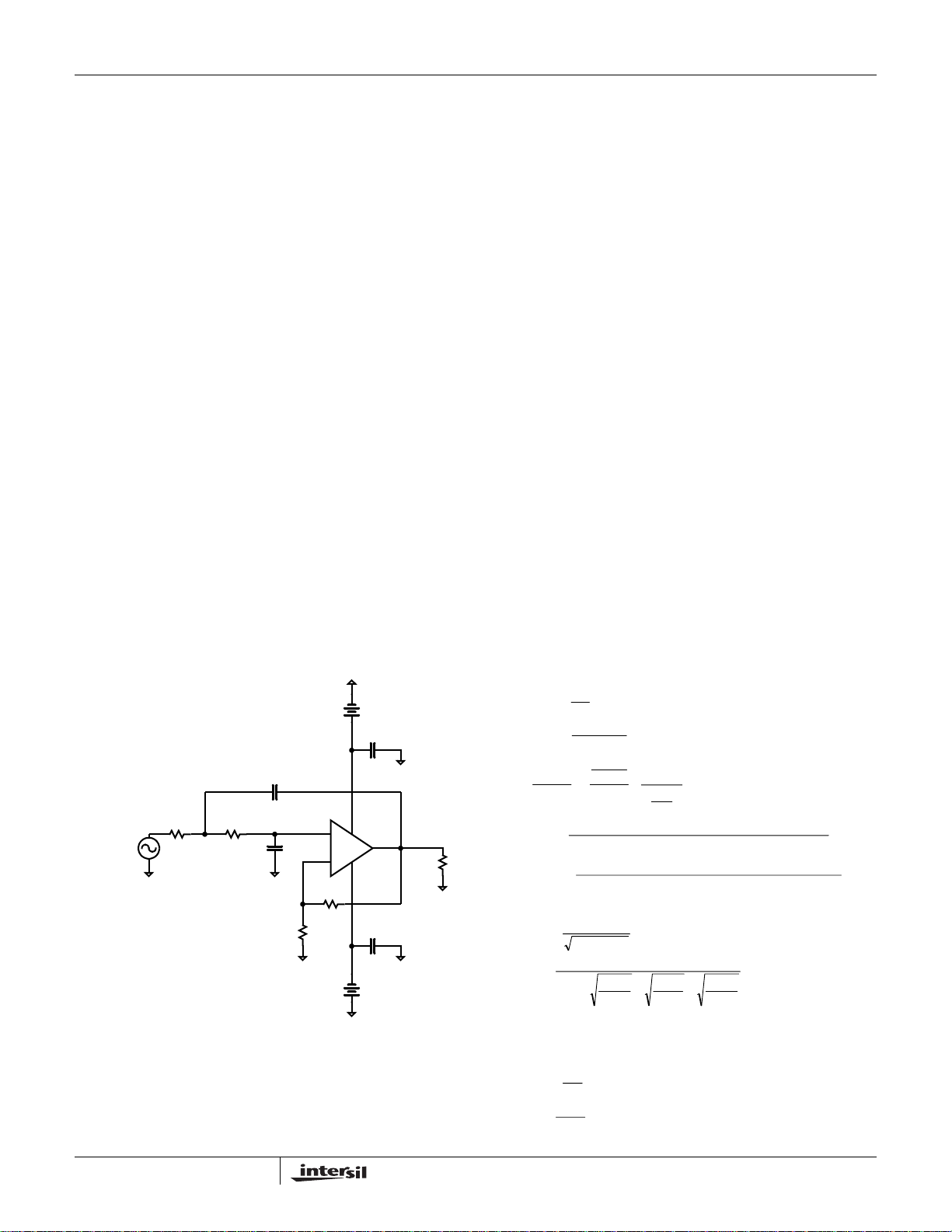
Choice of Feedback Resistor and Gain Bandwidth
Product
For applications that require a gain of +1, no feedback
resistor is required. Just short the output pin to the inverting
input pin. For gains greater than +1, the feedback resistor
forms a pole with the parasitic capacitance at the inverting
input. As this pole becomes smaller, the amplifier's phase
margin is reduced. This causes ringing in the time domain
and peaking in the frequency domain. Therefore, R
very big for optimum performance. If a large value of R
must be used, a small capacitor in the few Pico Farad range
in parallel with R
peaking at the expense of reducing the bandwidth. For gain
of +1, R
= 0 is optimum. For the gains other than +1,
F
optimum response is obtained with R
of R
and RG (see Figures15 and 16 for selection).
F
Video Performance
For good video performance, an amplifier is required to
maintain the same output impedance and the same
frequency response as DC levels are changed at the output.
This is especially difficult when driving a standard video load
of 150Ω, because of the change in output current with DC
level. The dG and dP of this device is about 0.01% and
0.05°, while driving 150Ω at a gain of 2. Driving high
impedance loads would give a similar or better dG and dP
performance.
Driving Capacitive Loads and Cables
The ISL55002 can drive a 47pF load in parallel with 500Ω
with less than 3dB of peaking at gain of +1 and as much as
100pF at a gain of +2 with under 3db of peaking. If less
peaking is desired in applications, a small series resistor
(usually between 5Ω to 50Ω) can be placed in series with the
output to eliminate most peaking. However, this will reduce
- pin) to 1.5V below the positive
S
can help to reduce the ringing and
F
with proper selection
F
can't be
F
F
the gain slightly. If the gain setting is greater than 1, the gain
resistor R
can then be chosen to make up for any gain loss
G
which may be created by the additional series resistor at the
output.
When used as a cable driver, double termination is always
recommended for reflection-free performance. For those
applications, a back-termination series resistor at the
amplifier's output will isolate the amplifier from the cable and
allow extensive capacitive drive. However, other applications
may have high capacitive loads without a back-termination
resistor. Again, a small series resistor at the output can help
to reduce peaking.
Output Drive Capability
The ISL55002 does not have internal short circuit protection
circuitry. It has a typical short circuit current of 140mA. If the
output is shorted indefinitely, the power dissipation could
easily overheat the die or the current could eventually
compromise metal integrity. Maximum reliability is
maintained if the output current never exceeds ±60mA. This
limit is set by the design of the internal metal interconnect.
Note that in transient applications, the part is robust.
Short circuit protection can be provided externally with a
back match resistor in series with the output placed close as
possible to the output pin. In video applications this would be
a 75Ω resistor and will provide adequate short circuit
protection to the device. Care should still be taken not to
stress the device with a short at the output.
Power Dissipation
With the high output drive capability of the ISL55002, it is
possible to exceed the 150°C absolute maximum junction
temperature under certain load current conditions.
Therefore, it is important to calculate the maximum junction
temperature for an application to determine if load conditions
or package types need to be modified to assure operation of
the amplifier in a safe operating area.
The maximum power dissipation allowed in a package is
determined according to:
T
–
PD
MAX
Where:
•T
JMAX
•T
AMAX
• θ
JA
The maximum power dissipation actually produced by an IC
is the total quiescent supply current times the total power
supply voltage, plus the power in the IC due to the load, or:
JMAXTAMAX
-------------------------------------------- -=
Θ
JA
= Maximum junction temperature
= Maximum ambient temperature
= Thermal resistance of the package
8
FN7497.4
July 27, 2006
Page 9
ISL55002
For sourcing:
PD
MAXVSISMAX
n
VSV
–()
∑
i1=
OUTi
V
-----------------
×+×=
OUTi
R
Li
For sinking:
n
V
–()
I
PD
MAXVSISMAX
∑
i1=
OUTiVS
×+×=
LOADi
Where:
•V
= Supply voltage
S
•I
•V
•R
•I
= Maximum quiescent supply current
SMAX
= Maximum output voltage of the application
OUT
= Load resistance tied to ground
LOAD
= Load current
LOAD
• N = number of amplifiers (max = 2)
By setting the two PD
can solve the output current and R
equations equal to each other, we
MAX
to avoid the device
LOAD
overheat.
Power Supply Bypassing Printed Circuit Board
Layout
As with any high frequency device, a good printed circuit
board layout is necessary for optimum performance. Lead
lengths should be as short as possible. The power supply
pin must be well bypassed to reduce the risk of oscillation.
For normal single supply operation, where the V
connected to the ground plane, a single 4.7µF tantalum
- pin is
S
capacitor in parallel with a 0.1µF ceramic capacitor from VS+
to GND will suffice. This same capacitor combination should
be placed at each supply pin to ground if split supplies are to
be used. In this case, the V
- pin becomes the negative
S
supply rail.
Printed Circuit Board Layout
For good AC performance, parasitic capacitance should be
kept to minimum. Use of wire wound resistors should be
avoided because of their additional series inductance. Use
of sockets should also be avoided if possible. Sockets add
parasitic inductance and capacitance that can result in
compromised performance. Minimizing parasitic capacitance
at the amplifier's inverting input pin is very important. The
feedback resistor should be placed very close to the
inverting input pin. Strip line design techniques are
recommended for the signal traces.
Application Circuits
Sallen Key Low Pass Filter
A common and easy to implement filter taking advantage of
the wide bandwidth, low offset and low power demands of
the ISL55002. A derivation of the transfer function is
provided for convenience (See Figure 28).
Sallen Key High Pass Filter
Again this useful filter benefits from the characteristics of the
ISL55002. The transfer function is very similar to the low
pass so only the results are presented (See Figure 29).
C
1
R
1
1kΩ
V
1
FIGURE 28. SALLEN-KEY LOW PASS FILTER
R
2
1kΩ C
1nF
2
1nF
R
1kΩ
V+
+
-
V-
R
B
1kΩ
A
V
2
5V
C
1nF
C
1nF
V
3
5V
B
R
1K
+=
A
R
1
V
KVo
5
=
1
1sCR
22
+
Vo
ViV
1
−
R
1
)s(H
V
OUT
R
1kΩ
7
=
)jw(H
=
5
wo
Q
=
=
=
wo
=
RC
Q
=
VK
1
−
1
+
R
2
2211
=
2
KHolp
1
2211
CRCR
11
CR
)K1(
22
CR
KHolp
1
Equations simplify if we let all
components be equal R=C
1
K3
−
ViVo
−
0
+
=
1
sC
1
K
2
1s)CRCRCR)K1((sCRCR
2212111
+++−+
1
)CRCRCR)K1((jwCRCRw1
2221112211
++−+−
1
21
CR
12
CR
22
CR
++−
11
CR
9
FN7497.4
July 27, 2006
Page 10

ISL55002
V
2
5V
C
5
R
1kΩ
1nF
V+
+
-
V-
B
C
1nF
V
5V
V
OUT
R
7
1kΩ
5
3
C
1
R
1
1kΩ
V
1
R
2
1kΩ C
1nF
2
1nF
R
1kΩ
A
FIGURE 29. SALLEN-KEY HIGH PASS FILTER
wo
Q
Holp
wo
Q
=
KHolp
1
=
=
=
2
=
RC
2
=
K4
−
2211
CRCR
1
11
CR
)K1(
22
CR
21
CR
++−
12
CR
K
−
K4
Equations simplify if we let
all components be equal R=C
22
CR
11
CR
Differential Output Instrumentation Amplifier
The addition of a third amplifier to the conventional three
amplifier instrumentation amplifier introduces the benefits of
differential signal realization, specifically the advantage of
using common-mode rejection to remove coupled noise and
ground potential errors inherent in remote transmission. This
configuration also provides enhanced bandwidth, wider
output swing and faster slew rate than conventional three
amplifier solutions with only the cost of an additional
amplifier and few resistors.
A
e
1
e
2
1
+
-
R
2
R
G
R
2
A
2
+
R
3
R
R
R
3
R
3
A
3
+
R
3
3
3
R
3
A
4
+
-
R
3
REF
e
3
o
+
e
o
-
eo4
e
e
BW
12R2RG⁄+()e1e2–()–= e
o3
21 2R2RG⁄+()e1e2–()–=
o
2f
C1 2,
------------------=
A
Di
12R2RG⁄+()e1e2–()=
o4
A
21 2R2RG⁄+()–=
Di
Strain Gauge
The strain gauge is an ideal application to take advantage of
the moderate bandwidth and high accuracy of the ISL55002.
The operation of the circuit is very straightforward. As the
strain variable component resistor in the balanced bridge is
subjected to increasing strain, its resistance changes,
resulting in an imbalance in the bridge. A voltage variation
from the referenced high accuracy source is generated and
translated to the difference amplifier through the buffer
stage. This voltage difference as a function of the strain is
converted into an output voltage.
FIGURE 30. DIFFERENTIAL OUTPUT AMPLIFIER
10
FN7497.4
July 27, 2006
Page 11

VARIABLE SUBJECT
+
R
V
0V
15
5
-
TO STRAIN
1kΩ
R
16
1kΩ1kΩ
1kΩ
ISL55002
R
1kΩ
17
R
1kΩ
18
FIGURE 31. STRAIN GAUGE
R
1kΩ
+
-
F
+
-
V+
V-
+
-
V
5V
C
1nF
C
1nF
V
5V
2
6
V
OUT
R
L
(V1+V2+V3+V4)
1kΩ
12
4
11
FN7497.4
July 27, 2006
Page 12

Small Outline Package Family (SO)
A
D
NN
(N/2)+1
ISL55002
h X 45°
PIN #1
E
C
SEATING
PLANE
0.004 C
E1
B
0.010 BM CA
I.D. MARK
1
e
0.010 BM CA
(N/2)
c
SEE DETAIL “X”
L1
H
A2
GAUGE
PLANE
A1
b
DETAIL X
L
4° ±4°
MDP0027
SMALL OUTLINE PACKAGE FAMILY (SO)
SYMBOL SO-8 SO-14
(0.150”)
A 0.068 0.068 0.068 0.104 0.104 0.104 0.104 MAX -
A1 0.006 0.006 0.006 0.007 0.007 0.007 0.007 ±0.003 A2 0.057 0.057 0.057 0.092 0.092 0.092 0.092 ±0.002 -
b 0.017 0.017 0.017 0.017 0.017 0.017 0.017 ±0.003 c 0.009 0.009 0.009 0.011 0.011 0.011 0.011 ±0.001 -
D 0.193 0.341 0.390 0.406 0.504 0.606 0.704 ±0.004 1, 3
E 0.236 0.236 0.236 0.406 0.406 0.406 0.406 ±0.008 -
E1 0.154 0.154 0.154 0.295 0.295 0.295 0.295 ±0.004 2, 3
e 0.050 0.050 0.050 0.050 0.050 0.050 0.050 Basic L 0.025 0.025 0.025 0.030 0.030 0.030 0.030 ±0.009 -
L1 0.041 0.041 0.041 0.056 0.056 0.056 0.056 Basic -
h 0.013 0.013 0.013 0.020 0.020 0.020 0.020 Reference -
N 8 14 16 16 20 24 28 Reference -
NOTES:
1. Plastic or metal protrusions of 0.006” maximum per side are not included.
2. Plastic interlead protrusions of 0.010” maximum per side are not included.
3. Dimensions “D” and “E1” are measured at Datum Plane “H”.
4. Dimensioning and tolerancing per ASME Y14.5M-1994
SO16
SO16 (0.300”)
(SOL-16)
SO20
(SOL-20)
SO24
(SOL-24)
SO28
(SOL-28) TOLERANCE NOTES
A
0.010
Rev. L 2/01
All Intersil U.S. products are manufactured, assembled and tested utilizing ISO9000 quality systems.
Intersil Corporation’s quality certifications can be viewed at www.intersil.com/design/quality
Intersil products are sold by description only. Intersil Corporation reserves the right to make changes in circuit design, software and/or specifications at any time without
notice. Accordingly, the reader is cautioned to verify that data sheets are current before placing orders. Information furnished by Intersil is believed to be accurate and
reliable. However, no responsibility is assumed by Intersil or its subsidiaries for its use; nor for any infringements of patents or other rights of third parties which may result
from its use. No license is granted by implicat ion or oth erwise u nde r any p a tent or p at ent r ights of Intersil or its subsidiaries.
For information regarding Intersil Corporation and its products, see www.intersil.com
12
FN7497.4
July 27, 2006
 Loading...