

Page 1

®
ISL54206A
Data Sheet June 25, 2007
MP3/USB 2.0 High Speed Switch with
Negative Signal Handling
The Intersil ISL54206A dual SPDT (Single Pole/Double
Throw) switches combine low distortion audio and accurate
USB 2.0 high speed data (480Mbps) signal switching in the
same low voltage device. When operated with a 2.7V to 3.6V
single supply these analog switches allow audio signal
swings below-ground, allowing the use of a common USB
and audio headphone connector in Personal Media Players
and other portable battery powered devices.
The ISL54206A logic control pins are 1.8V compatible which
allows for control via a standard µcontroller. With a VDD
voltage in the range of 2.7V to 3.6V the IN pin voltage can
exceed the VDD rail allowing for the USB 5V VBUS voltage
from a computer to directly drive the IN pin to switch
between the audio and USB signal sources in the portable
device. The part has an audio enable control pin to open all
the switches and put the part in a low power state.
The ISL54206A is available in a small 10 Ld 2.1mmx1.6mm
ultra-thin µTQFN package and a 10 Ld 3mmx3mm TDFN
package. It operates over a temperature range of -40 to
+85°C.
Related Literature
• Technical Brief TB363 “Guidelines for Handling and
Processing Moisture Sensitive Surface Mount Devices
(SMDs)”
• Application Note AN557 “Recommended Test Procedures
for Analog Switches”
FN6515.0
Features
• High Speed (480Mbps) and Full Speed (12Mbps)
Signaling Capability per USB 2.0
• Low Distortion Negative Signal Capability
• Control Pin to Open all Switches and Enter Low Power
State
• Low Distortion Headphone Audio Signals
- THD+N at 20mW into 32Ω Load . . . . . . . . . . . . . <0.1%
• Cross-talk Audio Channels (20Hz to 20kHz). . . . . -110dB
• Single Supply Operation (V
) . . . . . . . . . . . . 2.5V to 5.5V
DD
• -3dB Bandwidth USB Switches . . . . . . . . . . . . . . . 630MHz
• Available in µTQFN and TDFN Packages
• Pb-Free Plus Anneal (RoHS Compliant)
• Compliant with USB 2.0 Short Circuit Requirements
Without Additional External Components
Applications
• MP3 and Other Personal Media Players
• Cellular/Mobile Phones
•PDA’s
• Audio/USB Switching
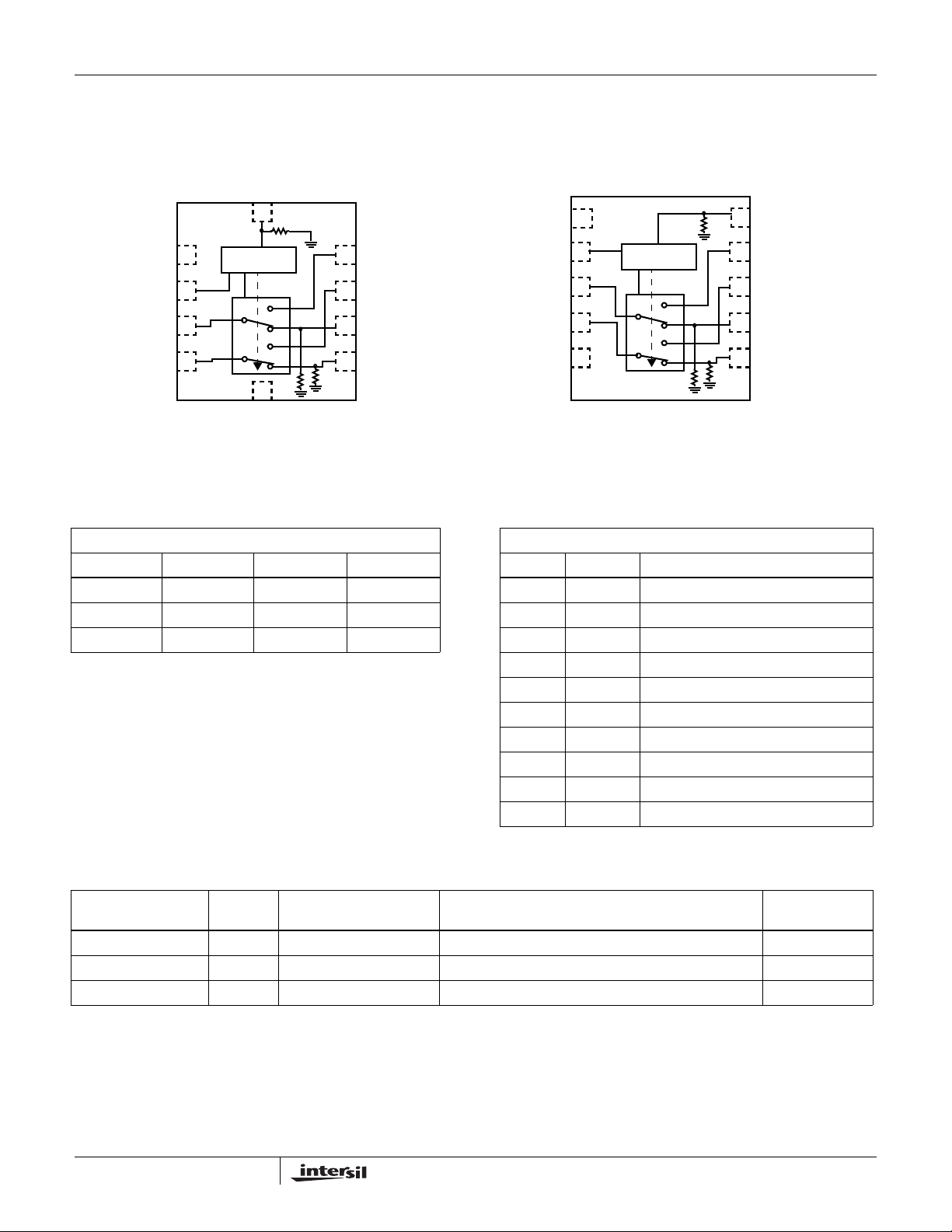
Application Block Diagram
VBUS
USB AND HEADPHONE JACK
1
IN
COM-
COM+
V
DD
ISL54206A
LOGIC CIRCUITRY
4MΩ
50kΩ
GND
CAUTION: These devices are sensitive to electrostatic discharge; follow proper IC Handling Procedures.
1-888-INTERSIL or 1-888-468-3774
50kΩ
µCONTROLLER
CTRL
USB
DD+
L
R
| Intersil (and design) is a registered trademark of Intersil Americas Inc.
All other trademarks mentioned are the property of their respective owners.
Copyright Intersil Americas Inc. 2007. All Rights Reserved
HIGH-SPEED
TRANSCEIVER
CODEC
Page 2
Pinouts (Note 1)
VDD
IN
COM -
1
2
3
ISL54206A
(10 LD µTQFN)
TOP VIEW
CTRL
10
4M
LOGIC
CONTROL
ISL54206A
ISL54206A
(10 LD TDFN)
TOP VIEW
VDD
1
IN
COM -
COM +
2
3
4
D-
9
D+
8
L
7
LOGIC
CONTROL
4M
CTRL
10
D-
9
D+
8
7
L
R
COM +
4
50k
5
GND
6
50k
NOTE:
1. ISL54206A Switches shown for IN = Logic “0” and CTRL = Logic “1”.
Truth Table
ISL54206A
IN CTRL L, R D+, D-
00OFFOFF
0 1 ON OFF
1XOFFON
IN: Logic “0” when ≤0.5V, Logic “1” when ≥1.4V with 2.7V to 3.6V
supply.
CTRL: Logic “0” when ≤0.5V or Floating, Logic “1” when ≥1.4V with
2.7V to 3.6V supply.
50k
6
R
GND
5
50k
Pin Descriptions
ISL54206A
PIN NO. NAME FUNCTION
1 VDD Power Supply
2 IN Digital Control Input
3 COM- Voice and Data Common Pin
4 COM+ Voice and Data Common Pin
5 GND Ground Connection
6 R Audio Right Input
7 L Audio Left Input
8 D+ USB Differential Input
9 D- USB Differential Input
10 CTRL Digital Control Input (Audio Enable)
Ordering Information
PART NUMBER
(Note)
ISL54206AIRTZ 06AZ -40 to +85 10 Ld 3mmx3mm TDFN L10.3x3A
ISL54206AIRTZ-T 06AZ -40 to +85 10 Ld 3mmx3mm TDFN Tape and Reel L10.3x3A
ISL54206AIRUZ-T FU -40 to +85 10 Ld Col µTQFN L10.2.1X1.6A
NOTE: Intersil Pb-free plus anneal products employ special Pb-free material sets; molding compounds/die attach materials and 100% matte tin plate
or NiPdAu termination finish, which are RoHS compliant and compatible with both SnPb and Pb-free soldering operations. Intersil Pb-free products
are MSL classified at Pb-free peak reflow temperatures that meet or exceed the Pb-free requirements of IPC/JEDEC J STD-020.
PART
MARKING TEMP. RANGE (°C) PACKAGE (Pb-Free) PKG. DWG. #
2
FN6515.0
June 25, 2007
Page 3

ISL54206A
Absolute Maximum Ratings Thermal Information
VDD to GND . . . . . . . . . . . . . . . . . . . . . . . . . . . . . . . . . -0.3 to 6.0V
Input Voltages
D+, D-, L, R (Note 2) . . . . . . . . . . . . . . . . . - 2V to ((V
IN (Note 2). . . . . . . . . . . . . . . . . . . . . . . . . . . . . . . . . . -2V to 5.5V
CTRL (Note 2). . . . . . . . . . . . . . . . . . . . . . -0.3 to ((V
) + 0.3V)
DD
) + 0.3V)
DD
Output Voltages
COM-, COM+ (Note 2) . . . . . . . . . . . . . . . . -2V to ((V
Continuous Current (Audio Switches). . . . . . . . . . . . . . . . . ±150mA
) + 0.3V)
DD
Peak Current (Audio Switches)
(Pulsed 1ms, 10% Duty Cycle, Max). . . . . . . . . . . . . . . . ±300mA
Continuous Current (USB Switches). . . . . . . . . . . . . . . . . . . ±40mA
Peak Current (USB Switches)
(Pulsed 1ms, 10% Duty Cycle, Max) . . . . . . . . . . . . . . . . ±100mA
ESD Rating:
HBM . . . . . . . . . . . . . . . . . . . . . . . . . . . . . . . . . . . . . . . . . . . >7kV
MM . . . . . . . . . . . . . . . . . . . . . . . . . . . . . . . . . . . . . . . . . . . >400V
CDM . . . . . . . . . . . . . . . . . . . . . . . . . . . . . . . . . . . . . . . . . .>1.4kV
CAUTION: Do not operate at or near the maximum ratings listed for extended periods of time. Exposure to such conditions may adversely impact product reliability and
result in failures not covered by warranty.
NOTES:
2. Signals on D+, D-, L, R, COM-, COM+, CTRL, IN exceeding V
ratings.
3. θ
is measured with the component mounted on a high effective thermal conductivity test board in free air. See Tech Brief TB379 for details.
JA
or GND by specified amount are clamped. Limit current to maximum current
DD
Thermal Resistance (Typical, Note 3) θ
(°C/W)
JA
10 Ld μTQFN Package . . . . . . . . . . . . . . . . . . . . . . . 130
10 Ld 3x3 TDFN Package. . . . . . . . . . . . . . . . . . . . . 110
Maximum Junction Temperature (Plastic Package) . . . . . . . +150°C
Maximum Storage Temperature Range . . . . . . . . . -65°C to +150°C
Pb-free reflow profile. . . . . . . . . . . . . . . . . . . . . . . . . . see link below
http://www.intersil.com/pbfree/Pb-FreeReflow.asp
Operating Conditions
Temperature Range . . . . . . . . . . . . . . . . . . . . . . . . . -40°C to +85°C
Electrical Specifications - 2.7V to 3.6V Supply Test Conditions: V
V
= 0.5V, (Notes 4), unless otherwise specified.
CTRLL
PARAMETER TEST CONDITIONS
ANALOG SWITCH CHARACTERISTICS
Audio Switches (L, R)
V
Analog Signal Range, V
ON Resistance, R
ON Resistance, R
ON Resistance, R
ON Resistance, R
R
Matching Between Channels,
ON
ΔR
ON
R
Flatness, R
ON
ANALOG
ON
ON
ON
ON
FLAT(ON)
Discharge Pull-Down Resistance,
, R
R
L
R
USB Switches (D+, D-)
Analog Signal Range, V
ON Resistance, R(
ANALOG
ON)
= 3.0V, IN = 0.5V, CTRL = 1.4V Full -1.5 - 1.5 V
DD
V
= 5.0V , IN = 0V , CTRL = VDD, I
DD
V
= -0.85V to 0.85V,
R
(See Figure 3)
V
= 4.2V , IN = 0V , CTRL = VDD, I
DD
V
= -0.85V to 0.85V,
R
COMx
COMx
=40mA, VL or
= 40mA, VL or
(See Figure 3)
V
= 2.85V, IN = 0V, CTRL = VDD, I
DD
COMx
or VR = -0.85V to 0.85V,
(See Figure 3)
V
= 3.0V , IN = 0.5V , CTRL = 1.4V, I
DD
or VR = -0.85V to 0.85V,
COMx
(See Figure 3)
V
= 3.0V, IN = 0.5V , CTR L = 1.4V, I
DD
or VR = Voltage at max R
over signal range of -0.85V
ON
COMx
to 0.85V, (Note 7)
V
= 3.0V , IN = 0.5V, CTRL = 1.4V, I
DD
COMx
or VR = -0.85V to 0.85V, (Note 6)
V
= 3.6V, IN = 0V, CTRL = 3.6V, V
DD
V
= -0.85V, 0.85V, VL or VR = -0.85V, 0.85V,
COM+
V
and VD- = floating, Measure current through the
D+
COM-
discharge pull-down resistor and calculate resistance
value.
V
= 3.6V, IN = 1.4V, CTRL = 1.4V Full 0 - V
DD
V
= 5.0V, IN = VDD, CTRL = VDD, I
DD
V
or V
D+
= 5V (See Figure 4)
D-
COMx
= +3.3V, GND = 0V, V
DD
TEMP
(°C)
25 - 2.47 - Ω
25 - 2.50 - Ω
= 40mA, V
= 40mA, V
25 - 2.87 - Ω
L
25 - 2.65 4.0 Ω
L
Full - - 5.5 Ω
= 40mA, V
25 - 0.02 0.13 Ω
L
Full - - 0.16 Ω
= 40mA, V
25 - 0.03 0.05 Ω
L
Full - - 0.07 Ω
or
= 1mA,
25 - 50 - kΩ
+25 - 17.7 - Ω
= 1.4V, V
INH
INL
MIN
(Notes 5, 8) TYP
= 0.5V, V
CTRLH
MAX
(Notes 5, 8) UNITS
DD
= 1.4V,
V
3
FN6515.0
June 25, 2007
Page 4

ISL54206A
Electrical Specifications - 2.7V to 3.6V Supply Test Conditions: V
V
= 0.5V, (Notes 4), unless otherwise specified. (Continued)
CTRLL
PARAMETER TEST CONDITIONS
ON Resistance, R(
ON Resistance, R(
ON Resistance, R(
ON Resistance, R
Matching Between Channels,
R
ON
ΔR
ON
R
Flatness, R
ON
OFF Leakage Current, I
I
D-(OFF)
ON Leakage Current, I
ON)
ON)
ON)
ON
FLAT(ON)
D+(OFF)
Dx
DYNAMIC CHARACTERISTICS
Turn-ON Tim e, t
Turn-OFF Time, t
ON
OFF
Break-Before-Make Time Delay, t
Skew, t
SKEW
Total Jitter, t
Propagation Delay, t
J
PD
Crosstalk (Channel-to-Channel),
R to COM-, L to COM+
Total Harmonic Distortion f = 20Hz to 20kHz, V
USB Switch -3dB Bandwidth Signal = 0dBm, 0.2V
D+/D- OFF Capacitance, C
C
D-(OFF)
L/R OFF Capacitance, C
C
ROFF
COM ON Capacitance, C
C
COM+(ON)
D+(OFF)
LOFF
COM-(ON)
POWER SUPPLY CHARACTERISTICS
Power Supply Range, V
Positive Supply Current, I
Positive Supply Current, I
Positive Supply Current, I
Positive Supply Current, I
DD
DD
DD
DD
DD
(Low Power State)
V
= 4.2V, IN = VDD, CTRL = VDD, I
DD
V
or V
D+
V
DD
V
D+
V
DD
V
D+
V
DD
V
D+
V
DD
I
COMx
signal range of 0V to 400mV, (Note 6)
V
DD
I
COMx
or
V
DD
V
COM+
V
= float
R
V
DD
V
D-
V
DD
V
DD
V
D
DD
V
DD
C
L
= 4.2V (See Figure 4)
D-
= 2.85V, IN = VDD, CTRL = VDD, I
or V
= 2.85V (See Figure 4)
D-
= 3.3V, IN = 1.4V, CTRL = 1.4V, I
or V
= 3.3V (See Figure 4)
D-
= 3.6V, IN = 1.4V, CTRL = 1.4V, I
or V
= 0V to 400mV (See Figure 4)
D-
= 3.6V, IN = 1.4V, CTRL = 1.4V,
= 40mA, V
D+
= 3.6V, IN = 1.4V, CTRL = 1.4V,
= 40mA, V
D+
= 3.6V, IN = 0V, CTRL = 3.6V, V
= 0.5V, 0V, V
= 3.3V, IN = 3.3V, CTRL = 0V or 3.3V, V
= 2.0V, V
COM- ,VCOM+
= 2.7V, RL = 50Ω, CL = 10pF, (See Figure 1) 25 - 67 - ns
= 2.7V, RL = 50Ω, CL = 10pF, (See Figure 1) 25 - 48 - ns
= 2.7V, RL = 50Ω, CL = 10pF, (See Figure 2) 25 - 18 - ns
= 3.3V, IN = 3.3V, CTRL = 0V or 3.3V, RL = 45Ω,
= 10pF, tR = tF= 750ps at 480Mbps,
(Duty Cycle = 50%) (See Figure 7)
V
= 3.3V, IN = 3.3V, CTRL = 0V or 3.3V, RL = 45Ω,
DD
C
= 10pF, tR = tF= 750ps at 480Mbps
L
V
= 3.3V, IN = 3.3V, CTRL = 0V or 3.3V, RL = 45Ω,
DD
C
= 10pF, (See Figure 7)
L
= 3.3V, IN = 0V, CTRL = 3.3V, RL = 32Ω,
V
DD
f = 20Hz to 20kHz, V
(See Figure 6)
V
or VR = 0.707V
,
L
,
f = 1MHz, V
V
or VD+ = V
D-
f = 1MHz, V
V
or VR = V
L
,
f = 1MHz, V
V
or VD+ = V
D-
V
= 3.6V, IN = 0V or 3.6V, CTRL = 3.6V 25 - 6 8 μA
DD
V
= 4.2V, IN = 0V or 4.2V, CTRL = 4.2V 25 - 6 - μA
DD
V
= 5.0V, IN = 0V or 5.0V, CTRL = 5.0V 25 - 8 - μA
DD
= 3.6V, IN = 0V, CTRL = 0V or float 25 - 1 7 nA
V
DD
RMS
= 3.3V, IN = 0V, CTRL = 3.3V,
DD
COMx
= 3.3V, IN = 0V, CTRL = 0V or 3.3V,
DD
= 0V, (See Figure 5)
COMx
= 3.3V, IN = 3.0V, CTRL = 0V or 3.3V,
DD
COMx
COMx
COMx
COMx
COMx
or V
= Voltage at m ax RONover
D-
or V
= 0V to 400mV, (Note 6)
D-
D+
or V
D-
COM-
= 0V, 0.5V, VL and
, VL and VR = float
or VL = 0.707V
R
= 3.0V, IN = 0V, CTRL = 3.0V,
DD
(2V
P-P
offset, RL = 50Ω, CL = 5pF 25 - 630 - MHz
DC
RMS
), RL = 32Ω
= 0V, (See Figure 5)
= 0V, (See Figure 5)
= +3.3V, GND = 0V, V
DD
TEMP
= 1mA,
= 1mA,
= 1mA,
= 40mA,
or
or
D+
(2V
),
P-P
INH
MIN
(°C)
(Notes 5, 8) TYP
= 1.4V, V
= 0.5V, V
INL
MAX
(Notes 5, 8) UNITS
CTRLH
= 1.4V,
+25 - 19.5 - Ω
+25 - 26 - Ω
+25 - 23.5 30 Ω
Full - - 35 Ω
25 - 4.6 5 Ω
Full - - 6.5 Ω
25 - 0.06 0.5 Ω
Full - - 0.55 Ω
25 - 0.4 0.6 Ω
Full - - 1.0 Ω
25 -10 - 10 nA
Full -70 - 70 nA
25 -10 2 10 nA
Full -75 - 75 nA
25 - 50 - ps
25 - 210 - ps
25 - 250 - ps
25 - -110 - dB
25 - 0.06 - %
25 - 6 - pF
25 - 9 - pF
25 - 10 - pF
Full 2.5 - 5.5 V
Full - - 10 μA
Full - - 140 nA
4
FN6515.0
June 25, 2007
Page 5

ISL54206A
Electrical Specifications - 2.7V to 3.6V Supply Test Conditions: V
V
= 0.5V, (Notes 4), unless otherwise specified. (Continued)
CTRLL
PARAMETER TEST CONDITIONS
= +3.3V, GND = 0V, V
DD
TEMP
(°C)
= 1.4V, V
INH
INL
MIN
(Notes 5, 8) TYP
= 0.5V, V
CTRLH
MAX
(Notes 5, 8) UNITS
DIGITAL INPUT CHARACTERISTICS
Voltage Low, V
Voltage High, V
Input Current, I
Input Current, I
Input Current, I
, V
INL
CTRLL
, V
INH
CTRLH
INL, ICTRLL
INH
CTRLH
CTRL Pull-Down Resistor, R
CTRLVDD
V
= 2.7V to 3.6V Full - - 0.5 V
DD
V
= 2.7V to 3.6V Full 1.4 - - V
DD
V
= 3.6V, IN = 0V, CTRL = 0V Full -50 20 50 nA
DD
V
= 3.6V, IN = 3.6V, CTRL = 0V Full -50 20 50 nA
DD
V
= 3.6V, IN = 0V, CTRL = 3.6V Full -2 1.1 2 μA
DD
= 3.6V, IN = 0V, CTRL = 3.6V Full - 4 - MΩ
NOTES:
4. V
= Input voltage to perform proper function.
LOGIC
5. The algebraic convention, whereby the most negative value is a minimum and the most positive a maximum, is used in this data sheet.
6. Flatness is defined as the difference between maximum and minimum value of on-resistance over the specified analog signal range..
matching between channels is calculated by subtracting the channel with the highest max RON value from the channel with lowest max
7. R
ON
R
value, between L and R or between D+ and D-.
ON
8. Parts are 100% tested at +25°C. Over temperature limits established by characterization and are not production tested.
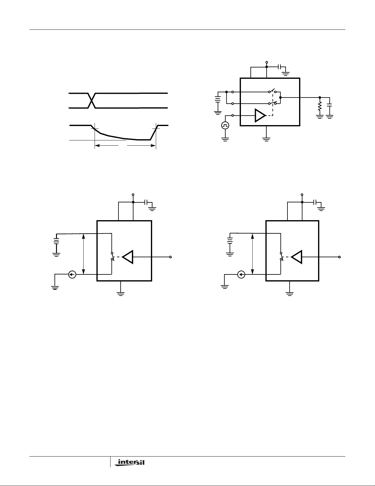
Test Circuits and Waveforms
DD
GND
C
COMx
R
L
------------------------------
RLR
+
ON()
RL
50Ω
V
OUT
LOGIC
INPUT
SWITCH
INPUT
SWITCH
OUTPUT
V
V
INPUT
DD
0V
0V
50%
t
ON
90%
t
OFF
V
OUT
tr <20ns
<20ns
t
f
90%
Logic input waveform is inverted for switches that have the opposite
logic sense.
V
CTRL
AUDIO or USB
IN
SWITCH
INPUT
V
IN
V
INPUT
Repeat test for all switches. CL includes fixture and stray
capacitance.
V
OUT
=
V
(INPUT)
= 1.4V,
C
L
10pF
FIGURE 1A. MEASUREMENT POINTS
5
FIGURE 1. SWITCHING TIMES
FIGURE 1B. TEST CIRCUIT
FN6515.0
June 25, 2007
Page 6
Test Circuits and Waveforms (Continued)
V
LOGIC
INPUT
DD
0V
ISL54206A
V
INPUT
CTRL
D- or D+
L or R
IN
V
DD
C
V
R
50Ω
OUT
C
L
L
10pF
COMx
SWITCH
OUTPUT
V
L OR R
V
OUT
0V
t
D
FIGURE 2A. MEASUREMENT POINTS
V
DD
RON = V1/100mA
100mA
V
1
CTRL
L OR R
COMx
GND
V
90%
IN
Repeat test for all switches. C
capacitance.
FIGURE 2. BREAK-BEFORE-MAKE TIME
C
V
D- OR D+
OV
IN
GND
L
FIGURE 2B. TEST CIRCUIT
RON = V1/40mA
V
1
40mA
includes fixture and stray
V
DD
C
CTRL
D- OR D+
IN
COMx
GND
VDD
Repeat test for all switches.
FIGURE 3. AUDIO R
Repeat test for all switches.
TEST CIRCUIT FIGURE 4. USB R
ON
6
TEST CIRCUIT
ON
FN6515.0
June 25, 2007
Page 7
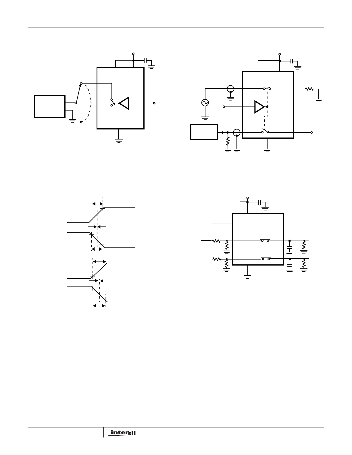
Test Circuits and Waveforms (Continued)
ISL54206A
V
DD
C
IMPEDANCE
ANALYZER
CTRL
AUDIO OR USB
COMx
GND
SIGNAL
GENERATOR
IN
0V or
V
DD
ANALYZER
0V
R
L
CTRL
L OR R
IN
COMx
GND
Repeat test for all switches.
Signal direction through switch is reversed, worst case values
are recorded. Repeat test for all switches.
FIGURE 5. CAPACITANCE TEST CIRCUIT FIGURE 6. AUDIO CROSSTALK TEST CIRCUIT
V
DD
C
GND
DIN+
DIN-
OUT+
OUT-
10%
90%
10%
90%
t
ri
90%
50%
V
DIN+
DIN-
DD
15.8Ω
143Ω
15.8Ω
143Ω
t
skew_i
50%
10%
t
fi
t
ro
90%
50%
t
skew_o
50%
10%
t
f0
tro - tri| Delay Due to Switch for Rising Input and Rising Output Signals.
|tfo - tfi| Delay Due to Switch for Falling Input and Falling Output Signals.
|tskew_0| Change in Skew through the Switch f or Output Signals.
|tskew_i| Change in Skew through the Switch for Input Signals.
CTRL
IN
COM+
COM-
FIGURE 7A. MEASUREMENT POINTS FIGURE 7B. TEST CIRCUIT
FIGURE 7. SKEW TEST
V
DD
COMx
R OR L
D+
D-
C
32Ω
NC.
OUT+
45Ω
CL
OUT-
45Ω
CL
7
FN6515.0
June 25, 2007
Page 8

Application Block Diagrams
ISL54206A
VDD
VBUS
USB AND HEADPHONE JACK
VBUS
22kΩ
IN
COM-
COM+
LOGIC CONTROL VIA MICRO-PROCESSOR
IN
4MΩ
COM-
ISL54206A
LOGIC CIRCUITRY
4MΩ
GND
VDD
ISL54206A
LOGIC CIRCUITRY
4MΩ
50kΩ
50kΩ
CTRL
D-
D+
L
R
CTRL
D-
D+
μCONTROLLER
USB
HIGH-SPEED
TRANSCEIVER
CODEC
μCONTROLLER
USB
HIGH-SPEED
TRANSCEIVER
COM+
USB AND HEADPHONE JACK
GND
LOGIC CONTROL VIA VBUS VOLTAGE FROM COMPUTER OR USB HUB
Detailed Description
The ISL54206A device is a dual single pole/double throw
(SPDT) analog switch device that can operate from a single
dc power supply in the range of 2.5V to 5.5V. It was
designed to function as a dual 2 to 1 multiplexer to select
between USB differential data signals and audio L and R
stereo signals. It comes in tiny µTQFN and TDFN packages
for use in MP3 players, PDAs, cell phones, and other
personal media players.
The part consists of two 3Ω audio switches and two 5Ω USB
switches. The audio switches can accept signals that swing
below ground. They were designed to pass audio left and
right stereo signals, that are ground referenced, with minimal
distortion. The USB switches were designed to pass
high-speed USB differential data signals with minimal edge
and phase distortion.
50kΩ
50kΩ
L
R
CODEC
The ISL54206A was specifically designed for MP3 players,
cell phones and other personal media player applications
that need to combine the audio headphone jack and the
USB data connector into a single shared connector, thereby
saving space and component cost. Typical application block
diagrams of this functionality is shown above.
The ISL54206A has a single logic control pin (IN) that
selects between the audio switches and the USB switches.
This pin can be driven Low or High to switch between the
audio CODEC drivers and USB transceiver of the MP3
player or cellphone. The ISL54206A also contains a logic
control pin (CTRL) that when driven Low while IN is Low,
opens all switches and puts the part into a low power state,
drawing typically 1nA of I
current.
DD
A detailed description of the two types of switches is
provided in the sections following. The USB transmission
8
FN6515.0
June 25, 2007
Page 9

ISL54206A
and audio playback are intended to be mutually exclusive
operations.
Audio Switches
The two audio switches (L, R) are 3Ω switches that can pass
signals that swing below ground by as much as 1.5V. They
were designed to pass ground reference stereo signals with
minimal insertion loss and very low distortion. Crosstalk
between the audio switches over the audio band is < -110dB.
Over a signal range of ±1V (0.707Vrms) with V
these switches have an extremely low r
ON
>2.7V,
DD
resistance
variation. They can pass ground referenced audio signals
with very low distortion (<0.06% THD+N) when delivering
15.6mW into a 32Ω
headphone speaker load. See Figures 8,
Figures 9, Figures 10, and Figures 11 THD+N performance
curves.
These switches are uni-directional switches. The audio
drivers should be connected at the L and R side of the switch
(pin 7 and pin 8) and the speaker loads should be connected
at the COM side of the switch (pin 3 and pin 4).
The audio switches are active (turned ON) whenever the IN
voltage is
≤0.5V and the CTRL voltage to ≥1.4V.
Note: Whenever the audio switches are ON the USB
transceivers need to be in the high impedance state or static
high or low state.
USB Switches
The two USB switches (D+, D-) are bidirectional switches
that can pass rail-to-rail signals. When powered with a 3.6V
supply these switches have a nominal r
signal range of 0V to 400mV with a r
The r
matching between the D+ and D- switches over
(ON)
this signal range is only 0.06Ω ensuring minimal impact by
the switches to USB high speed signal transitions. As the
signal level increases the r
resistance increases. At
(ON)
signal level of 3.3V the switch resistance is nominally 23Ω.
The USB switches were specifically designed to pass USB
2.0 high-speed (480Mbps) differential signals typically in the
range of 0V to 400mV. They have low capacitance and high
bandwidth to pass the USB high-speed signals with
minimum edge and phase distortion to meet USB 2.0 high
speed signal quality specifications. See high-speed eye
diagram Figure 15.
The USB switches can also pass USB full-speed signals
(12Mbps) with minimal distortion and meet all the USB
requirements for USB 2.0 full-speed signaling. See fullspeed eye diagram Figures 12-14.
The maximum signal range for the USB switches is from
-1.5V to V
allow to exceed the V
. The signal voltage at D- and D+ should not be
DD
voltage rail or go below ground by
DD
more than -1.5V.
of 4.6Ω over the
(ON)
flatness of 0.4Ω.
(ON)
The USB switches are active (turned ON) whenever the IN
voltage is
≥1.4V.
Note: Whenever the USB switches are ON the audio drivers
of the CODEC need to be at AC or DC ground or floating to
keep from interfering with the data transmission.
ISL54206A Operation
The discussion that follows will discuss using the ISL54206A
in the typical application shown in the block diagrams on
page 8.
VDD SUPPLY
The DC power supply connected at VDD (pin 1) provides the
required bias voltage for proper switch operation. The part
can operate with a supply voltage in the range of 2.5V to
5.5V.
In a typical USB/Audio application for portable battery
powered devices the V
an LDO and be in the range of 2.7V to 3.6V. For best
possible USB full-speed operation (12Mbps) it is
recommended that the V
a USB data signal level above 2.5V.
LOGIC CONTROL
The state of the ISL54206A device is determined by the
voltage at the IN pin (pin 2) and the CTRL pin (pin 10). Refer
to truth-table on page 2 of data sheet. These logic pins are
1.8V logic compatible when V
3.6V and can be controlled by a standard
The CTRL pin is internally pulled low through a 4MΩ resistor to
ground and can be left floating or tri-stated by the µprocessor.
The CTRL control pin is only active when IN is logic “0”.
The IN pin does not have an internal pull-down resistor and
must not be allowed to float. It must be driven High or Low.
The voltage at the IN pin can exceed the V
much as 2.55V. This allows the VBUS voltage from a
computer or USB hub (4.4V to 5.25V) to drive the IN pin
while the VDD voltage is in the range of 2.7V to 3.6V. An
external pull-down resistor is required from the IN pin to
ground when directly driving the IN pin with the computer
VBUS voltage. See the section titled “USING THE
COMPUTER VBUS VOLTAGE TO DRIVE THE “IN’ PIN”.
Logic control voltage levels:
IN = Logic “0” (Low) when IN
IN = Logic “1” (High) when IN
CTRL = Logic “0” (Low) when
CTRL = Logic “1” (High) when
Audio Mode
If the IN pin = Logic “0” and CTRL pin = Logic “1,” the part
will be in the Audio mode. In Audio mode the L (left) and R
(right) 3Ω audio switches are ON and the D- and D+ 5Ω USB
switches are OFF (high impedance).
voltage will come from a battery or
DD
voltage be ≥2.5V in order to get
DD
is in the range of 2.7V to
DD
≤0.5V
≥1.4V
≤0.5V or floating.
≥1.4V
μprocessor.
voltage by as
DD
9
FN6515.0
June 25, 2007
Page 10

ISL54206A
When nothing is plugged into the common connector or a
headphone is plugged into the common connector, the
μprocessor will sense that there is no voltage at the VBUS
pin of the connector and will drive and hold the IN control pin
of the ISL54206A low. As long as the CTRL = Logic “1,” the
ISL54206A part will be in the audio mode and the audio
drivers of the media player can drive the headphones and
play music.
USB Mode
If the IN pin = Logic “1” and CTRL pin = Logic “0” or Logic “1”
the part will go into USB mode. In USB mode, the D- and D+
5Ω switches are ON and the L and R 3Ω audio switches are
OFF (high impedance).
When a USB cable from a computer or USB hub is
connected at the common connector, the
μprocessor will
sense the present of the 5V VBUS and drive the IN pin
voltage high. The ISL54206A part will go into the USB mode.
In USB mode, the computer or USB hub transceiver and the
MP3 player or cell phone USB transceiver are connected
and digital data will be able to be transmitted back and forth.
When the USB cable is disconnected, the
μprocessor will
sense that the 5V VBUS voltage is no longer connected and
will drive the IN pin low and put the part back into the Audio
or Low Power Mode.
Low Power Mode
If the IN pin = Logic “0” and CTRL pin = Logic “0,” the part will
be in the Low Power mode. In the Low Power mode, the audio
switches and the USB switches are OFF (high impedance). In
this state, the device draws typically 1nA of current.
USING THE COMPUTER VBUS VOLTAGE TO DRIVE THE
“IN” PIN
computer or USB hub (4.4V to 5.25V) to drive the IN pin
while the V
voltage is in the range of 2.7V to 3.6V.
DD
External IN Series Resistor
The ISL54206A contains a clamp circuit between IN and
VDD. Whenever the IN voltage is greater than the VDD
voltage by more than 2.55V, current will flow through this
clamp circuitry into the V
During normal USB operation, V
power supply bus.
DD
is in the range of 2.7V to
DD
3.6V and IN (VBUS voltage from computer or USB hub) is in
the range of 4.4V to 5.25V , the clamp circuit is not active and
no current will flow through the clamp into the V
In a USB application, the situation can exist where the V
DD
supply.
BUS
voltage from the computer could be applied at the IN pin
before the V
range and current will flow through the clamp into the V
voltage is up to its normal operating voltage
DD
DD
power supply bus. This current could be quite high when
V
is OFF or at 0V and could potentially damage other
DD
components connected in the circuit. In the application
circuit, a 22kΩ resistor has been put in series with the IN pin
to limit the current to a safe level during this situation.
It is recommended that a current limiting resistor in the range
of 10kΩ to 50kΩ be connected in series with the IN pin. It will
have minimal impact on the logic level at the IN pin during
normal USB operation and protect the circuit during the time
VBUS is present before VDD is up to its normal operating
voltage.
Note: No external resistor is required in applications where
the voltage at the IN pin will not exceed V
by more than
DD
2.55V.
External IN Pull-Down Resistor
Rather than using a micro-processor to control the IN logic
pin you can directly drive the IN pin using the VBUS voltage
from the computer or USB hub. In order to do this you must
connected an external resistor from the IN pin to ground.
When a headphone or nothing is connected at the common
connector the external pull-down will pull the IN pin low
putting the ISL54206A in the Audio mode or Low Power
mode depending on the condition of the CTRL pin.
When a USB cable is connected at the common connector
the voltage at the IN pin will be driven to 5V and the part will
automatically go into the USB mode.
When the USB cable is disconnected from the common
connector the voltage at the IN pin will be pulled low by the
pull-down resistor and return to the Audio Mode or Low
Power Mode depending on the condition of the CTRL pin.
Note: The voltage at the IN pin can exceed the VDD voltage
by as much as 2.55V. This allows the VBUS voltage from a
10
FN6515.0
June 25, 2007
Page 11

ISL54206A
Typical Performance Curves T
0.11
R
= 32Ω
LOAD
= 0.707V
V
LOAD
0.1
0.09
0.08
0.07
THD+N (%)
0.06
0.05
0.04
VDD = 2.6V
VDD = 2.7V
20 200 2k 20k
RMS
VDD = 3V
FREQUENCY (Hz)
= +25°C, Unless Otherwise Specified
A
VDD = 3.6V
FIGURE 8. THD+N vs SUPPLY VOLTAGE vs FREQUENCY
0.5
R
= 32Ω
LOAD
= 1kHz
FREQ
=3V
V
DD
0.4
0.4
R
= 32Ω
LOAD
= 3V
V
DD
3V
0.3
0.2
THD+N (%)
0.1
0
20 200 2k 20k
P-P
2.5V
P-P
2V
P-P
1V
P-P
FREQUENCY (Hz)
FIGURE 9. THD+N vs SIGNAL LEVELS vs FREQUENCY
0.5
R
= 32Ω
LOAD
= 1kHz
FREQ
=3V
V
DD
0.4
0.3
THD+N (%)
0.2
0.1
0
00.511.522.533.5
OUTPUT VOLTAGE (V
P-P
)
0.3
0.2
THD+N (%)
0.1
0
0 1020304050
OUTPUT POWER (mW)
FIGURE 10. THD+N vs OUTPUT VOLTAGE FIGURE 11. THD+N vs OUTPUT POWER
11
FN6515.0
June 25, 2007
Page 12

ISL54206A
Typical Performance Curves T
VOLTAGE SCALE (0.5V/DIV)
= +25°C, Unless Otherwise Specified (Continued)
A
VDD=5.5V
TIME SCALE (10ns/DIV)
FIGURE 12. EYE PATTERN: 12MBps WITH SWITCHES IN THE SIGNAL PATH
12
FN6515.0
June 25, 2007
Page 13
ISL54206A
Typical Performance Curves T
VOLTAGE SCALE (0.5V/DIV)
= +25°C, Unless Otherwise Specified (Continued)
A
VDD=3.3V
TIME SCALE (10ns/DIV)
FIGURE 13. EYE PATTERN: 12MBps WITH SWITCHES IN THE SIGNAL PATH
13
FN6515.0
June 25, 2007
Page 14

ISL54206A
Typical Performance Curves T
VOLTAGE SCALE (0.5V/DIV)
= +25°C, Unless Otherwise Specified (Continued)
A
VDD=2.5V
TIME SCALE (10ns/DIV)
FIGURE 14. EYE PATTERN: 12MBps WITH SWITCHES IN THE SIGNAL PATH
14
FN6515.0
June 25, 2007
Page 15

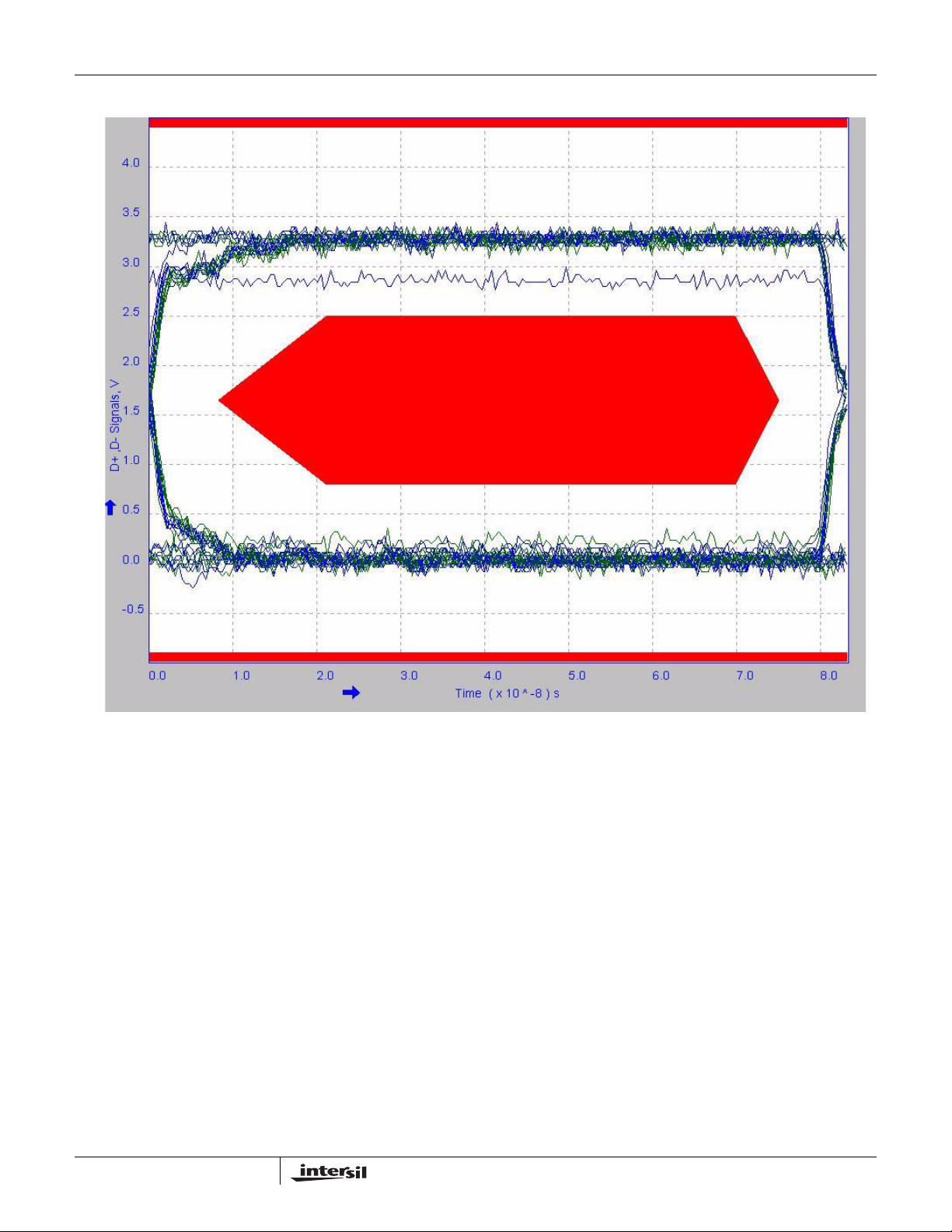
ISL54206A
Typical Performance Curves T
VOLTAGE SCALE (0.1V/DIV)
= +25°C, Unless Otherwise Specified (Continued)
A
VDD = 3.3V
V
= 3.3V
DD
FIGURE 15. EYE PATTERN: 480MBps USB SIGNAL WITH SWITCHES IN THE SIGNAL PATH
1
0
-1
-2
-3
-4
NORMALIZED GAIN (dB)
RL = 50Ω
VIN = 0.2V
1M 10M 100M 1G
P-P
to 2V
P-P
FREQUENCY (Hz)
USB SWITCH
FIGURE 16. FREQUENCY RESPONSE
15
TIME SCALE (0.2ns/DIV.)
Die Characteristics
SUBSTRATE POTENTIAL (POWERED UP):
GND (TDFN Paddle Connection: Tie to GND or Float)
TRANSISTOR COUNT:
98
PROCESS:
Submicron CMOS
FN6515.0
June 25, 2007
Page 16

ISL54206A
Ultra Thin Quad Flat No-Lead Plastic Package (UTQFN)
INDEX AREA
PIN #1 ID
NX (b)
5
SECTION "C-C"
6
2X
0.10 C
2X
0.10 C
0.10 C
0.05 C
SEATING PLANE
(DATUM A)
1
N
N-1
(A1)
D
N
21
TOP VIEW
A
A1
SIDE VIEW
2
e
(ND-1) X e
BOTTOM VIEW
NX L
(DATUM B)
NX b
0.10 M C A B
3
CC
FOR ODD TERMINAL/SIDE
0.05 M C
C
L
e
b
A
B
E
4xk
5
L
TERMINAL TIP
L10.2.1x1.6A
10 LEAD ULTRA THIN QUAD FLAT NO-LEAD PLASTIC
PACKAGE
MILLIMETERS
SYMBOL
A 0.45 0.50 0.55 A1 - - 0.05 A3 0.127 REF -
b 0.15 0.20 0.25 5
C
D 2.05 2.10 2.15 -
E 1.55 1.60 1.65 -
e 0.50 BSC -
k0.20
---
L 0.35 0.40 0.45 -
N102
Nd 4 3
Ne 1 3
θ
0-12
NOTES:
1. Dimensioning and tolerancing conform to ASME Y14.5-1994.
2. N is the number of terminals.
3. Nd and Ne refer to the number of terminals on D and E side,
respectively.
4. All dimensions are in millimeters. Angles are in degrees.
5. Dimension b applies to the metallized terminal and is measured
between 0.15mm and 0.30mm from the terminal tip.
6. The configuration of the pin #1 identifier is optional, but must be
located within the zone indicated. The pin #1 identi fier may be
either a mold or mark feature.
7. Maximum package warpage is 0.05mm.
8. Maximum allowable burrs is 0.076mm in all directions.
9. Same as JEDEC MO-255UABD except:
No lead-pull-back, "A" MIN dimension = 0.45 not 0.50mm
"L" MAX dimension = 0.45 not 0.42mm.
10. For additional information, to assist with the PCB Land Pattern
Design effort, see Intersil Technical Brief TB389.
NOTESMIN NOMINAL MAX
4
Rev. 3 6/06
0.10 MIN
0.05 MIN
DETAIL “A” PIN 1 ID
16
2.50
1.75
L
2.00
0.275
0.50
0.25
LAND PATTERN
0.80
10
FN6515.0
June 25, 2007
Page 17

ISL54206A
Thin Dual Flat No-Lead Plastic Package (TDFN)
(DAT UM B )
6
INDEX
AREA
(DATUM A)
NX (b)
5
SECTION "C-C"
6
INDEX
AREA
SEATING
PLANE
NX L
8
A
C
D
TOP VIEW
SIDE VIEW
D2
D2/2
12
N
N-1
e
(Nd-1)Xe
REF .
BOTTOM VIEW
(A1)
2X
A3
E2/2
NX b
5
C
L
e
CC
FOR ODD TERMINAL/SIDE
E
A
87
NX k
E2
0.10
ABC0.10
2X
0.10
//
M
TERMINAL TIP
0.10
0.08
L1
CB
BAC
L10.3x3A
10 LEAD THIN DUAL FLAT NO-LEAD PLASTIC PACKAGE
MILLIMETERS
SYMBOL
A
A1
A3
b
D
D2
E
C
C
E2
e
k
L
N
Nd
0.70 0.75 0.80
- - 0.05
0.20 REF
0.20 0.25 0.30
2.95 3.0 3.05
2.25 2.30 2.35
2.95 3.0 3.05
1.45 1.50 1.55
0.50 BSC
0.25 - -
0.25 0.30 0.35
10
5
NOTES:
1. Dimensioning and tolerancing conform to ASME Y14.5-1994.
2. N is the number of terminals.
3. Nd refers to the number of terminals on D.
4. All dimensions are in millimeters. Angles are in degrees.
5. Dimension b applies to the metallized terminal and is measured
between 0.15mm and 0.30mm from the terminal tip.
6. The configuration of the pin #1 identifier is optional, but must be
located within the zone indicated. The pin #1 identi fier may be
either a mold or mark feature.
7. Dimensions D2 and E2 are for the exposed pads which provide
improved electrical and thermal performance.
8. Nominal dimensions are provided to assist with PCB Land
Pattern Design efforts, see Intersil Technical Brief TB389.
9. Compliant to JEDEC MO-229-WEED-3 except for D2
dimensions.
L
9
NOTESMIN NOMINAL MAX
-
-
-
5, 8
-
7, 8
-
7, 8
-
8
2
3
Rev. 3 3/06
All Intersil U.S. products are manufactured, assembled and tested utilizing ISO9000 quality systems.
Intersil Corporation’s quality certifications can be viewed at www.intersil.com/design/quality
Intersil products are sold by description only. Intersil Corporation reserves the right to make changes in circuit design, software and/or specifications at any time without
notice. Accordingly, the reader is cautioned to verify that data sheets are current before placing orders. Information furnished by Intersil is believed to be accurate and
reliable. However, no responsibility is assumed by Intersil or its subsidiaries for its use; nor for any infringements of patents or other rights of third parties which may result
from its use. No license is granted by implicat ion or oth erwise u nde r any p a tent or p at ent r ights of Intersil or its subsidiaries.
For information regarding Intersil Corporation and its products, see www.intersil.com
17
FN6515.0
June 25, 2007
 Loading...