

®
ISL54200
Data Sheet January 24, 2007
USB 2.0 High/Full Speed Multiplexer
The Intersil ISL54200 dual 2:1 multiplexer IC is a single
supply part that can operate from a single 2.7V to 5.5V supply .
It contains two SPDT (Single Pole/Double Throw) switches
configured as a DPDT. The part was designed for switching
between USB High-Speed and USB Full-Speed sources in
portable battery powered products.
The 7
Ω normally-closed (NC) FSx switches can swing rail to
rail and were specifically designed to pass USB full speed
data signals (12Mbps) that range from 0V to 3.6V. The 4.5
normally-open (NO) HSx switches have high bandwidth and
low capacitance and were specifically designed to pass USB
high speed data signals (480Mbps) with minimal di stortion.
The part can be used in Personal Media Players and other
portable battery powered devices that need to switch between
a high-speed transceiver and a full-speed transceiver while
connected to a single USB host (computer).
The digital logic inputs are 1.8V logic compatible when
operated with a 2.7V to 3.6V supply. The part has an enable
pin to open all switches. It can be used to facilitate pro per bus
disconnect and connection when switching between the USB
sources.
The ISL54200 is available in a 10 Ld 3mmx3mm TDFN and a
small 10 Ld 2.1mmx1.6mm µTQFN packages. It operates
over a temperature range of -40 to +85°C.
Ω
FN6408.0
Features
• High Speed (480Mbps) and Full Speed (12Mbps)
Signaling Capability per USB 2.0
• 1.8V Logic Compatible (2.7V to +3.6V supply)
• Enable Pin to Open all Switches
• -3dB Frequency
- HSx Switches. . . . . . . . . . . . . . . . . . . . . . . . . . . . .880MHz
- FSx Switches. . . . . . . . . . . . . . . . . . . . . . . . . . . . .550MHz
• Cross-talk @ 1MHz . . . . . . . . . . . . . . . . . . . . . . . . . -70dB
• OFF Isolation @ 100kHz . . . . . . . . . . . . . . . . . . . . . -98dB
• Single Supply Operation (V
• Available in Ultra-thin
) . . . . . . . . . . . . 2.7V to 5.5V
DD
µTQFN and TDFN Packages
• Pb-Free Plus Anneal (RoHS Compliant)
Applications
• MP3 and other Personal Media Players
• Cellular/Mobile Phones
•PDA’s
• Digital Cameras and Camcorders
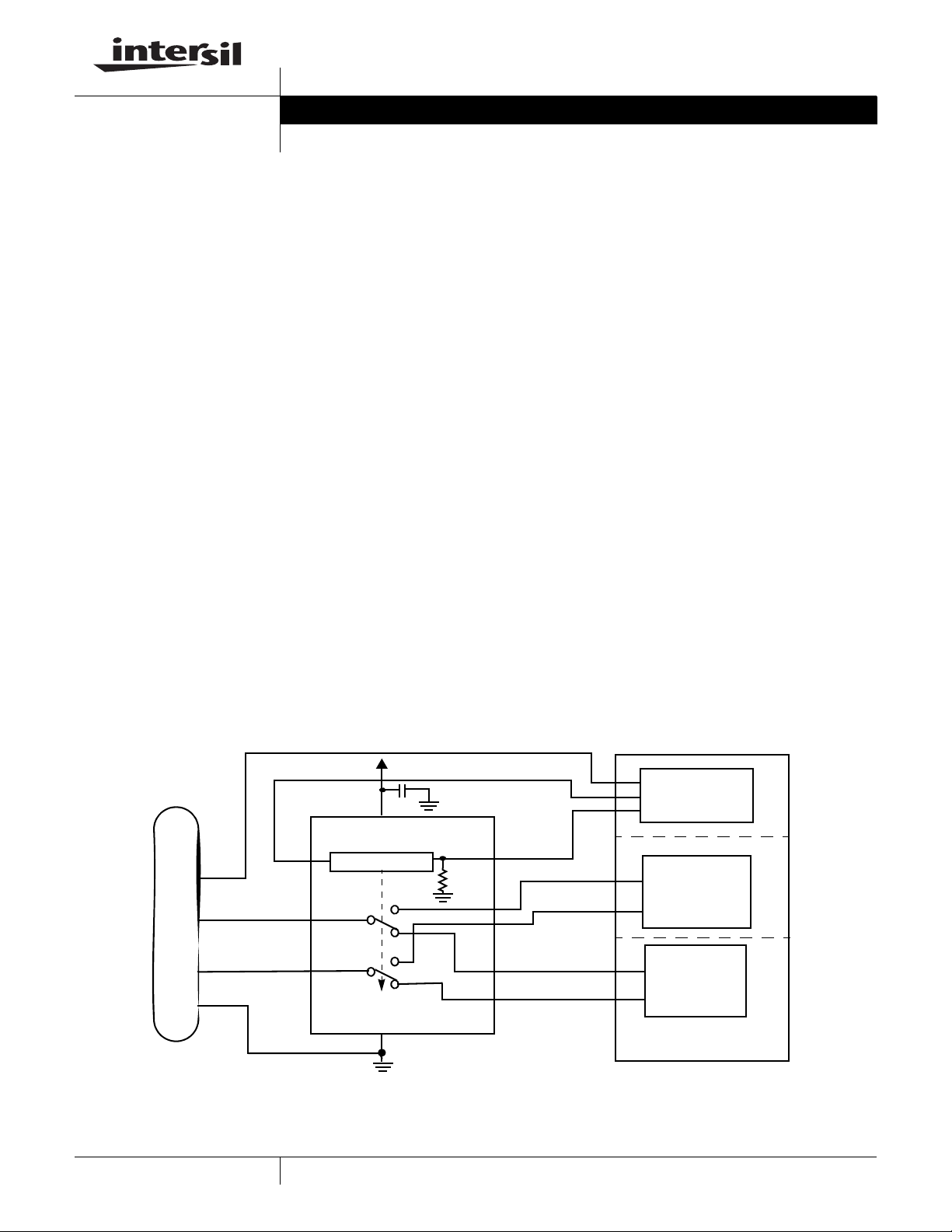
Application Block Diagram
VBUS
D-
D+
USB CONNECTOR
GND
3.3V
V
IN
ISL54200
LOGIC CIRCUITRY
COMD1
COMD2
GND
DD
EN
4MΩ
HSD1
HSD2
FSD1
FSD2
µCONTROLLER
USB
HIGH-SPEED
TRANSCEIVER
USB
FULL-SPEED
TRANSCEIVER
PORTABLE MEDIA DEVICE
1
CAUTION: These devices are sensitive to electrostatic discharge; follow proper IC Handling Procedures.
1-888-INTERSIL or 1-888-468-3774
| Intersil (and design) is a registered trademark of Intersil Americas Inc.
All other trademarks mentioned are the property of their respective owners.
Copyright Intersil Americas Inc. 2007. All Rights Reserved
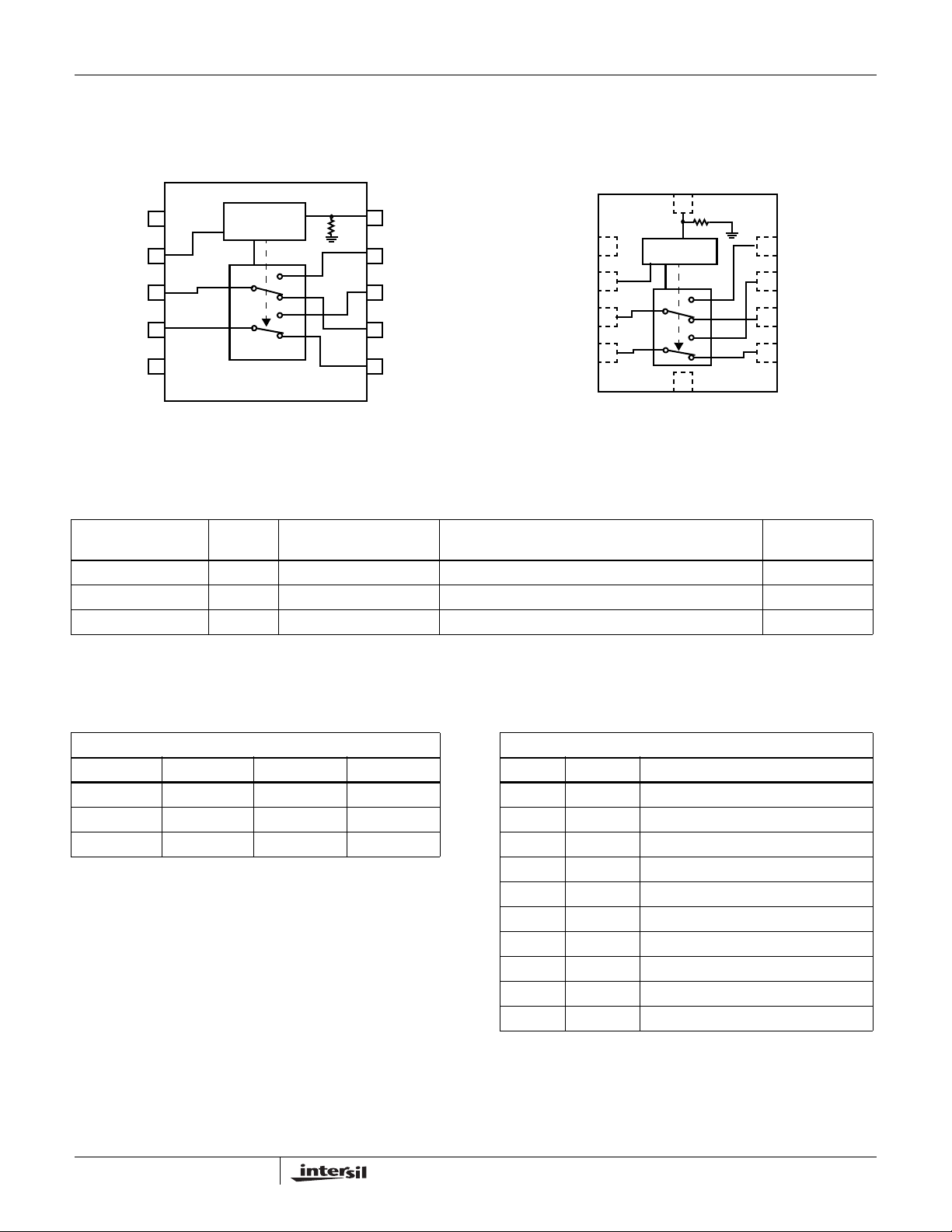
Pinouts
ISL54200
(10 LD TDFN
TOP VIEW
VDD
COMD1
COMD2
GND
1
IN
2
3
4
5
LOGIC
CONTROL
4M
EN
10
9
HSD1
8
HSD2
7
FSD1
6
FSD2
NOTE:
1. ISL54200 Switches Shown for IN = Logic “0” and EN = Logic “1”.
Ordering Information
ISL54200
VDD
COMD1
COMD2
ISL54200
(10 LD µTQFN)
TOP VIEW
EN
10
4M
HSD1
1
IN
2
3
4
LOGIC
CONTROL
5
GND
9
HSD2
8
FSD1
7
FSD2
6
PART NUMBER
(Note)
PART
MARKING TEMP. RANGE (°C) PACKAGE (Pb-Free) PKG. DWG. #
ISL54200IRZ 200Z -40 to +85 10 Ld 3x3 TDFN L10.3x3A
ISL54200IRZ-T 200Z -40 to +85 10 Ld 3x3 TDFN Tape and Reel L10.3x3A
ISL54200IRUZ-T FM -40 to +85 10 Ld 2.1x1.6mm μTQFN Tape and Reel L10.2.1x1.6A
NOTE: Intersil Pb-free plus anneal products employ special Pb-free material sets; molding compounds/die attach materials and 100% matte tin plate
termination finish, which are RoHS compliant and compatible with both SnPb and Pb-free soldering operations. Intersil Pb-free products are MSL
classified at Pb-free peak reflow temperatures that meet or exceed the Pb-free requirements of IPC/JEDEC J STD-020.
Truth Table
ISL54200
EN IN FSD1, FSD2 HSD1, HSD2
1 0 ON OFF
11OFFON
0XOFFOFF
Logic “0” when ≤0.5V, Logic “1” when ≥1.4V with a 2.7V to 3.6V
Supply. X = Don’t Care
Pin Descriptions
ISL54200
PIN NO. NAME FUNCTION
1 VDD Power Supply
2 IN Select Logic Control Input
3 COMD1 USB Common Port
4 COMD2 USB Common Port
5 GND Ground Connection
6 FSD1 Full Speed USB Differential Port
7 FSD2 Full Speed USB Differential Port
8 HSD1 High Speed USB Differential Port
9 HSD2 High Speed USB Differential Port
10 EN Bus Switch Enable
2
FN6408.0
January 24, 2007
ISL54200
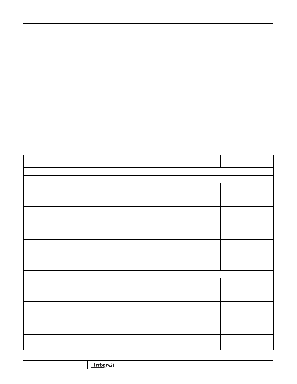
Absolute Maximum Ratings Thermal Information
VDD to GND . . . . . . . . . . . . . . . . . . . . . . . . . . . . . . . . . -0.3 to 6.0V
Input Voltages
FSD2, FSD1, HSD2, HSD1 (Note 2) . . . . . - 1V to ((V
IN, EN (Note 2). . . . . . . . . . . . . . . . . . . . . . . -0.3 to ((V
Output Voltages
DD
DD
) +0.3V)
) +0.3V)
COMD1, COMD2 (Note 2) . . . . . . . . . . . . . . . . . . . . . . . -1V to 5V
Continuous Current (HSD2, HSD1, FSD2, FSD1). . . . . . . . . ±40mA
Peak Current (HSD2, HSD1, FSD2, FSD1)
(Pulsed 1ms, 10% Duty Cycle, Max) . . . . . . . . . . . . . . . . ±100mA
ESD Rating:
HBM . . . . . . . . . . . . . . . . . . . . . . . . . . . . . . . . . . . . . . . . . . . .>7kV
MM . . . . . . . . . . . . . . . . . . . . . . . . . . . . . . . . . . . . . . . . . . .>400V
CDM. . . . . . . . . . . . . . . . . . . . . . . . . . . . . . . . . . . . . . . . . . >1.4kV
CAUTION: Stresses above those listed in “Absolute Maximum Ratings” may cause permanent damage to the device. This is a stress only rating and operation of the
device at these or any other conditions above those indicated in the operational sections of this specification is not implied.
NOTES:
2. Signals on FSD1, FSD2, HSD1, HSD2, COMD1, COMD2, EN, IN exceeding V
maximum current ratings.
3. θ
is measured with the component mounted on a high effective thermal conductivity test board in free air. See Tech Brief TB379 for details.
JA
Thermal Resistance (Typical, Note 3) q
(°C/W)
JA
10 Ld 3x3 TDFN Package . . . . . . . . . . . . . . . . . . . . 55
10 Ld µTQFN Package . . . . . . . . . . . . . . . . . . . . . . 140
Maximum Junction Temperature (Plastic Package). . . . . . . +150°C
Maximum Stor age Temperatur e Range. . . . . . . . . . . -65°C to +150°C
Operating Conditions
Temperature Range
ISL54200IRZ and ISL54200IRUZ . . . . . . . . . . . . . . -40°C to +85°C
V
Supply Voltage Range. . . . . . . . . . . . . . . . . . . . . 2.7V to 5.5V
DD
or GND by specified amount are clamped. Limit current to
DD
Electrical Specifications - 2.7V to 3.6V Supply Test Conditions: V
V
= 0.5V, (Notes 4, 6), Unless Otherwise Specified
ENL
PARAMETER TEST CONDITIONS
ANALOG SWITCH CHARACTERISTICS
NC Switches (FSD1, FSD2)
Analog Signal Range, V
ON Resistance, r
Matching Between Channels,
r
(ON)
Δr
(ON)
r
Flatness, r
(ON)
OFF Leakage Current, I
ON Leakage Current, I
ANALOG
(ON)
FLAT(ON)
FSX(OFF)
FSX(ON)
NO Switches (HSD1, HSD2)
Analog Signal Range, V
ON Resistance, r
ON Resistance, r
Matching Between Channels,
r
(ON)
Δr
(ON)
Flatness, r
r
(ON)
ANALOG
(ON)
(ON)
FLAT(ON)
V
= 3.3V, IN = 0V, EN = 3.3V Full 0 - V
DD
V
= 3.3V, IN = 0.5V, EN = 1.4V, I
DD
V
or V
FSD1
V
= 3.3V, IN = 0.5V, EN = 1.4V, I
DD
V
or V
FSD1
= 0V to 3.3V, (See Figure 4)
FSD2
= Voltage at ma x r
FSD2
= 40mA,
COMx
= 40mA,
COMx
over signal range
(ON)
of 0V to 3.3V, (Note 8)
V
= 3.3V, IN = 0.5V, EN = 1.4V, I
DD
V
FSD1
or V
= 0V to 3.3V, (Note 7)
FSD2
COMx
= 40mA,
V+ = 3.6 V, IN = 3.6V, EN = 0V and 3.6V, V
3V , V
V+ = 3.6V, IN = 0V, EN = 3.6V, V
V
V
V
V
V
V
V
V
r
V
V
= 3V, 0.3V
FSX
= 0.3V, 3V,
= 0.3V, 3V
FSX
= 3.3V, IN = 3.3V, EN = 3.3V Full 0 - V
DD
= 3.3V, IN = 1.4V, EN = 1.4V, I
DD
or V
HSD2
= 3.3V, IN = 1.4V, EN = 1.4V, I
DD
or V
HSD2
= 3.3V, IN = 1.4V, EN = 1.4V, I
DD
or V
HSD2
over signal range of 0V to 400mV (Note 8)
(ON)
= 3.3V, IN = 1.4V, EN = 1.4V, I
DD
or V
HSD2
= 3.3V (See Figure 3)
HSD1
= 0V to 400mV (See Figure 3)
HSD1
= Voltage at max r
HSD1
= 0V to 400mV, (Note 7)
HSD1
COMx
COMx
COMx
COMx
, Voltage at max
(ON)
COMx
= 1mA,
= 40mA,
= 40mA,
= 40mA,
= +3.3V, GND = 0V, V
DD
= 0.3V,
COMx
TEMP
(°C)
= 1.4V, V
INH
MIN
(Note 5) TYP
= 0.5V, V
INL
= 1.4V,
ENH
MAX
(Note 5) UNITS
DD
+25 - 7 10 Ω
Full - - 15 Ω
+25 - 0.1 0.35 Ω
Full - - 0.4 Ω
+25 - 4 6 Ω
Full - - 8 Ω
+25 -20 2 20 nA
Full -70 - 70 nA
+25 -20 2 20 nA
Full -70 - 70 nA
DD
+25 - 20 30 Ω
Full - - 35 Ω
+25 - 4.5 6 Ω
Full - - 8 Ω
+25 - 0.01 0.1 Ω
Full - - 0.5 Ω
+25 - 0.4 1 Ω
Full - - 1.5 Ω
V
V
3
FN6408.0
January 24, 2007
ISL54200
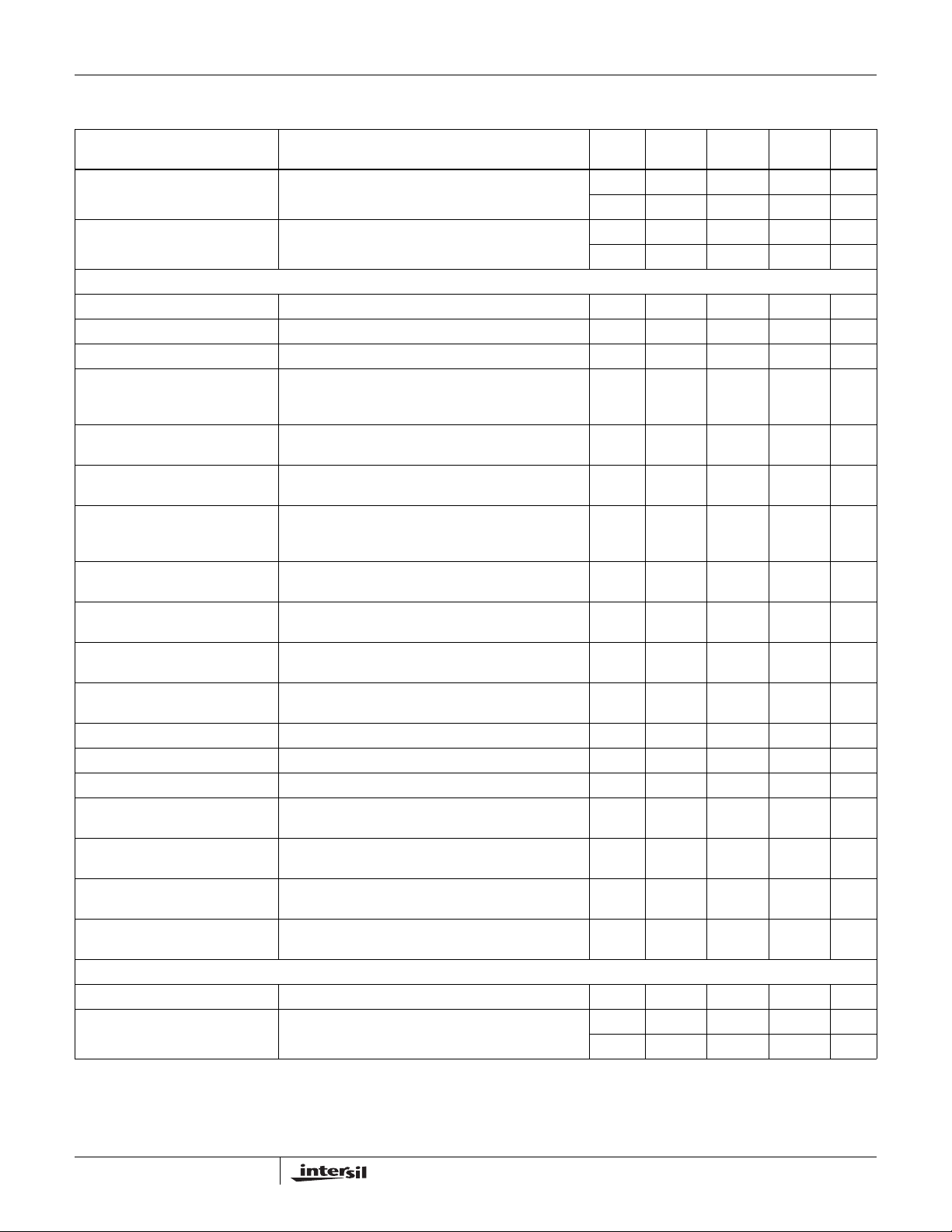
Electrical Specifications - 2.7V to 3.6V Supply Test Conditions: V
V
= 0.5V, (Notes 4, 6), Unless Otherwise Specified (Continued)
ENL
PARAMETER TEST CONDITIONS
OFF Leakage Current, I
or I
HSD1(OFF)
ON Leakage Current, I
I
HSD1(ON)
HSD2(OFF)
HSD2(ON)
DYNAMIC CHARACTERISTICS
Turn-ON Time, t
Turn-OFF Time, t
ON
OFF
Break-Before-Make Time Delay, t
Skew, t
SKEW
(HSx Switch)
Total Jitter, t
J
(HSx Switch)
Propagation Delay, t
(HSx Switch)
Skew, t
SKEW
PD
(FSx Switch)
Rise
/Fall Time Mismatch, t
(FSx Switch)
Total Jitter, t
(FSx Switch)
Propagation Delay, t
(FSx Switch)
J
PD
Crosstalk V
OFF Isolation V
FSx Switch -3dB Bandwidth Signal = -10dBm, 1.0VDC offset, R
HSx Switch -3dB Bandwidth Signal = -10dBm, 0.2VDC offset, R
HSx OFF Capacitance, C
FSx OFF Capacitance, C
COM ON Capacitance, C
COM ON Capacitance, C
HSxOFF
FSxOFF
COMX(ON)
COMX(ON)
POWER SUPPLY CHARACTERISTICS
Power Supply Range, V
Positive Supply Current, I
DD
DD
V
= 3.6V , IN = 0V, EN = 0 and 3.6V, V
DD
V
or
V
V
V
V
V
D
V
t
R
(See Figure 7)
V
t
R
V
(See Figure 7)
V
t
R
(See Figure 7)
M
V
t
R
V
t
R
V
(See Figure 7
= 3V, 0.3V, V
COMD2
= 3.6V, IN = 3.6V, EN = 3.6V, V
DD
= 0.3V, 3.0V, V
COMD2
= 3.3V, RL = 45Ω, CL = 10pF, (See Figure 1) +25 - 25 - ns
DD
= 3.3V, RL = 45Ω, CL = 10pF, (See Figure 1) +25 - 15 - ns
DD
= 3.3V, RL = 45Ω, CL = 10pF, (See Figure 2) +25 -7-ns
DD
= 3.3V , IN = 3.3V, EN = 3.3V , RL = 45Ω, CL = 10pF ,
DD
HSD2
HSD2
or V
or V
= tF= 720ps at 480Mbps, (Duty Cycle = 50%)
=3.3V , IN = 3.3V, EN = 3.3V, RL = 45Ω, CL = 10pF,
DD
= tF= 720ps at 480Mbps
= 3.3V , IN = 3.3V, EN = 3.3V , RL = 45Ω, CL = 10pF ,
DD
= 3.3V, IN = 0V, EN = 3.3V, RL = 39Ω, CL = 50pF,
DD
= tF = 12ns at 12Mbps, (Duty Cycle = 50%)
= 3.3V, IN = 0V, EN = 3.3V, RL = 39Ω, CL = 50pF,
DD
= tF = 12ns at 12Mbps, (Duty Cycle = 50%)
= 3.3V, IN = 0V, EN = 3.3V, RL = 39Ω, CL = 50pF,
DD
= tF = 12ns at 12Mbps
= 3.3V, IN = 0V, EN = 3.3V, RL = 39Ω, CL = 50pF,
DD
= 3.3V, RL = 45Ω, f = 1MHz
DD
HSD1
HSD1
COMD1
= 0.3V, 3V
COMD1
= 0.3V , 3.0V
(See Figure 6)
= 3.3V, RL = 45Ω, f = 100kHz +25 - -98 - dB
DD
= 45Ω, CL = 5pF +25 - 880 - MHz
L
= 45Ω, CL = 5pF +25 - 550 - MHz
L
f = 1MHz, V
V
= V
HSD2
f = 1MHz, V
V
FSD2
f = 1MHz, V
V
= V
HSD2
f = 1MHz, V
V
= V
FSD2
V
= 3.6V, IN = 0V or 3.6V, EN = 0V or 3.6V +25 - 20 60 nA
DD
= 3.3V, IN = 0V, EN = 3.3V, V
DD
= 0V, (See Figure 5)
COMx
= 3.3V, IN = 3.3V, EN = 3.3V, V
DD
= V
= 0V, (See Figure 5)
COMx
= 3.3V, IN = 3.3V, EN = 3.3V, V
DD
= 0V, (See Figure 5)
COMx
= 3.3V, IN = 0V, EN = 3.3V, V
DD
= 0V, (See Figure 5)
COMx
= +3.3V, GND = 0V, V
DD
TEMP
(°C)
or
+25 -20 2 20 nA
Full -70 - 70 nA
or
+25 -20 2 20 nA
Full -70 - 70 nA
+25 - 50 - ps
+25 - 210 - ps
+25 - 250 - ps
+25 - 0.15 - ns
+25 - 10 - %
+25 - 1.6 - ns
+25 - 0.9 - ns
+25 - -70 - dB
HSD1
FSD1
HSD1
FSD1
or
or
+25 - 6 - pF
or
+25 - 9 - pF
or
+25 - 12 - pF
+25 - 15 - pF
Full 2.7 - 5.5 V
Full - - 80 nA
= 1.4V, V
INH
INL
MIN
(Note 5) TYP
= 0.5V, V
ENH
MAX
(Note 5) UNITS
= 1.4V,
4
FN6408.0
January 24, 2007
ISL54200
Electrical Specifications - 2.7V to 3.6V Supply Test Conditions: V
V
= 0.5V, (Notes 4, 6), Unless Otherwise Specified (Continued)
ENL
PARAMETER TEST CONDITIONS
= +3.3V, GND = 0V, V
DD
TEMP
(°C)
= 1.4V, V
INH
INL
MIN
(Note 5) TYP
= 0.5V, V
ENH
MAX
(Note 5) UNITS
DIGITAL INPUT CHARACTERISTICS
Input Voltage Low, V
Input Voltage High, V
Input Current, I
Input Current, I
Input Current, I
INL, IENL
INH
ENH
INL
INH
, V
, V
ENL
ENH
V
= 2.7V to 3.6V Full - - 0.5 V
DD
V
= 2.7V to 3.6V Full 1.4 - - V
DD
V
= 3.6V, IN = 0V, EN = 0V Full - 10 - nA
DD
V
= 3.6V, IN = 3.6 Full - 10 - nA
DD
V
= 3.6V, EN = 3.6 Full - 1 - μA
DD
NOTES:
4. V
= Input voltage to perform proper function.
LOGIC
5. The algebraic convention, whereby the most negative value is a minimum and the most positive a maximum, is used in this data sheet.
6. Parameters with limits are 100% tested at +25°C. Limits across the full temperature range are guaranteed by design and correlation.
7. Flatness is defined as the difference between maximum and minimum value of on-resistance over the specified analog signal range
matching between channels is calculated by subtracting the channel with the highest max r
8. r
(ON)
r
value, between HSD2 and HSD1 or between FSD2 and FSD1.
(ON)
value from the channel with lowest max
(ON)
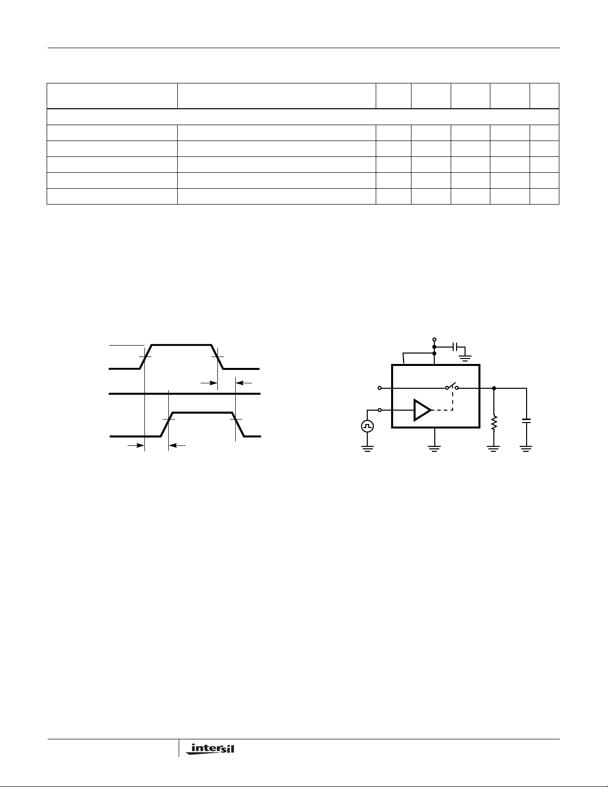
Test Circuits and Waveforms
V
tr < 20ns
< 20ns
t
f
90%
LOGIC
INPUT
SWITCH
INPUT
SWITCH
OUTPUT
VIN
VIN
V
INPUT
0V
H
50%
L
t
OFF
V
OUT
90%
t
ON
Logic input waveform is inverted for switches that have the opposite
logic sense.
FIGURE 1A. MEASUREMENT POINTS
FIGURE 1. SWITCHING TIMES
V
SWITCH
INPUT
INPUT
VIN
Repeat test for all switches. C
capacitance.
V
OUT
FIGURE 1B. TEST CIRCUIT
DD
EN
HSx or FSx
IN
V
=
(INPUT)
COMx
GND
includes fixture and stray
L
R
----------------------------
RLr
+
RL
45W
L
ON()
V
OUT
= 1.4V,
C
L
10pF
5
FN6408.0
January 24, 2007

Test Circuits and Waveforms (Continued)
ISL54200
V
DD
C
LOGIC
INPUT
SWITCH
OUTPUT
V
OUT
V
HSX
VIN
H
VIN
L
0V
t
D
FIGURE 2A. MEASUREMENT POINTS
V
r
= V1/I
(ON)
COMx
HSx
V
90%
Repeat test for all switches. CL includes fixture and stray
capacitance.
FIGURE 2. BREAK-BEFORE-MAKE TIME
DD
C
INPUT
VIN
V
FSX
r
(ON)
EN
FSD1 or FSD2
HSD1 or HSD2
IN
GND
FIGURE 2B. TEST CIRCUIT
= V1/40mA
FSx
COMx
V
OUT
R
L
45Ω
V
DD
C
C
L
10pF
V
1
I
COMx
Repeat test for all switches.
FIGURE 3. HSx Switch r
COMx
GND
1.4V
TEST CIRCUIT
(ON)
EN
IN
1.4V
V
40mA
Repeat test for all switches.
FIGURE 4. FSx Switch r
1
COMx
GND
TEST CIRCUIT
(ON)
EN
1.4V
IN
0.5V
6
FN6408.0
January 24, 2007
Test Circuits and Waveforms (Continued)
V
DD
C
ISL54200
V
DD
C
IMPEDANCE
ANALYZER
Repeat test for all switches.
FIGURE 5. CAPACITANCE TEST CIRCUIT
DIN+
DIN-
OUT+
OUT-
10%
90%
10%
90%
FIGURE 7A. MEASUREMENT POINTS
HSx or FSx
COMx
t
ri
50%
50%
t
fi
t
ro
50%
50%
t
f0
90%
10%
t
skew_i
90%
t
skew_o
10%
EN
GND
IN
VINL OR
VIN
H
FIGURE 7. SKEW TEST
SIGNAL
GENERATOR
ANALYZER
IN
VIN
R
L
HSx
COMx
EN
GND
FSx
COMx
45Ω
Signal direction through switch is reversed, worst case values
are recorded. Repeat test for all switches.
FIGURE 6. CROSSTALK TEST CIRCUIT
V
DD
C
EN
DIN+
DIN-
VIN
15.8Ω
143Ω
15.8Ω
143Ω
VIN
COMD2
COMD1
GND
D2
D1
CL
CL
OUT+
45Ω
OUT-
45Ω
|tro-tri| Delay Due to Switch for Rising Input and Rising Output
Signals.
|tfo-tfi| Delay Due to Switch for Falling Input and Falling Output
Signals.
|tskew_0| Change in Skew through the Switch for Output Signals.
|tskew_i| Change in Skew through the Switch for Input Signals.
FIGURE 7B. TEST CIRCUIT
N.C.
7
FN6408.0
January 24, 2007

Application Block Diagram
VBUS
D-
3.3V
V
IN
ISL54200
LOGIC CIRCUITRY
COMD1
DD
ISL54200
EN
4MΩ
HSD1
HSD2
µCONTROLLER
USB
HIGH-SPEED
TRANSCEIVER
D+
USB CONNECTOR
GND
COMD2
GND
Detailed Description
The ISL54200 device is a dual single pole/double throw
(SPDT) analog switch that operates from a single DC power
supply in the range of 2.7V to 5.5V. It was designed to
function as dual 2-to-1 multiplexer to select between a USB
high-speed transceiver and a USB full-speed transceiver in
portable battery powered products. It is offered in a TDFN
package and a small µTQFN package for use in MP3
players, cameras, PDAs, cellphones, and other personal
media players. The device has an enable pin to open all
switches.
The part consist of two 7Ω full speed (FSx) switches and two
4.5Ω high speed (HSx) switches. The FSx switches can
swing from 0V to V
speed (12Mbps) differential data signals with minimal
distortion. The HSx switches have high bandwidth and low
capacitance to pass USB high-speed (480Mbps) differential
data signals with minimal edge and phase distortion.
The ISL54200 was designed for MP3 players, cameras,
cellphones, and other personal media player applications
that have both high-speed and full-speed transceivers and
need to multiplex between these USB sources to a single
USB host (computer). A typical application block diagram of
this functionality is shown above.
A detailed description of the two types of switches are
provided in the sections below.
FSx Switches (FSD1, FSD2)
The two FSx switches (FSD1, FSD2) are bidirectional
switches that can pass rail-to-rail signals. When powered
with a 3.3V supply, these switches have a nominal r
resistance of 7Ω over the signal range of 0V to 3.3V. They
. They were designed to pass USB full-
DD
(ON)
FSD1
FSD2
PORTABLE MEDIA DEVICE
USB
FULL-SPEED
TRANSCEIVER
were specifically designed to pass USB full-speed (12Mbps)
differential signals and meet the USB 2.0 full-speed signal
quality specifications. See eye diagram Figure 8.
The FSx switches can also pass USB high speed signals
(480Mbps) but do not quite meet the USB 2.0 high speed
signal quality eye diagram compliance requirement.
The maximum signal range for the FSx switches is from
-1.5V to V
exceed the V
. The signal voltage should not be allowed to
DD
voltage rail or go below ground by more
DD
than -1.5V.
When operated with a 2.7V to 3.6V supply, the FSx switches
are active (turned ON) whenever the IN logic control voltage
is
≤0.5V and the EN logic voltage ≥1.4V.
HSx Switches (HSD1, HSD2)
The two HSx switches (HSD2, HSD1) are bidirectional
switches that can pass rail-to-rail signals. When powered
with a 3.3V supply these switches have a nominal r
4.5Ω over the signal range of 0V to 400mV with a r
flatness of 0.4Ω. The r
HSD2 switches over this signal range is only 0.01Ω ensuring
minimal impact by the switches to USB high speed signal
transitions. As the signal level increases the r
resistance increases. At signal level of 3.3V the switch
resistance is nominally 20Ω.
The HSx switches were specifically designed to pass USB
2.0 high-speed (480Mbps) differential signals typically in the
range of 0V to 400mV. They have low capacitance and high
bandwidth to pass the USB high-speed signals with
minimum edge and phase distortion to meet USB 2.0 high
speed signal quality specifications. See high-speed eye
diagrams Figures 9 and 10.
matching between the HSD1 and
(ON)
(ON)
of
(ON)
(ON)
switch,
8
FN6408.0
January 24, 2007

ISL54200
The HSx switches can also pass USB full-speed signals
(12Mbps) with minimal distortion and meet all the USB
requirements for USB 2.0 full-speed signaling. See fullspeed eye diagram Figure 11.
The maximum signal range for the HSx switches is from
-1.5V to V
exceed the V
. The signal voltage should not be allow to
DD
voltage rail or go below ground by more
DD
than -1.5V.
The HSx switches are active (turned ON) whenever the IN
voltage is
≥1.4V and the EN logic voltage ≥1.4V when
operated with a 2.7V to 3.6V supply.
ISL54200 Operation
The discussion that follows will discuss using the ISL54200 in
the typical application shown in the block diagram on page 9.
POWER
The power supply connected at the VDD (pin 1) provides the
DC bias voltage required by the ISL54200 part for proper
operation. The ISL54200 can be operated with a VDD
voltage in the range of 2.7V to 5.5V. When used in a USB
application the VDD voltage should be kept in the range of
3.0V to 5.5V to ensure you get the proper signal levels for
good signal quality.
A 0.01µF or 0.1µF decoupling capacitor should be
connected from the VDD pin to ground to filter out any power
supply noise from entering the part. The capacitor should be
located as close to the VDD pin as possible.
computer. The device will be able to transmit and receive
data from the computer at a data rate of 12Mbps.
High-speed Mode
If the IN pin = Logic “1” and EN pin = Logic “1” the part will go
into high-speed mode. In high-speed mode the HSD1 and
HSD2 switches are ON and the FSD1 and FSD2 switches
are OFF (high impedance). When a USB cable from a
computer or USB hub is connected at the common USB
connector and the part is in the high-speed mode a link will
be established between the high-speed driver section of the
media player and the computer. The device will be able to
transmit and receive data fr om the computer at a data rate of
480Mbps.
All Switches OFF Mode
If the IN pin = Logic “0” or Logic “1” and EN pin = Logic “0” all
of the switches will turn OFF (high impedance).
The all OFF state can be used to switch between the two
USB sections of the media player. When disconnecting from
one USB device to the other USB device you can
momentarily put the ISL54400 switch in the “all off” state in
order to get the computer to disconnect from the one device
so it can properly connect to the other USB device when that
channel is turned ON.
LOGIC CONTROL
The state of the ISL54200 device is determined by the
voltage at the IN pin (pin 2) and the EN pin (pin 10). IN is
only active when the EN pin is logic “1” (High). Refer to“Truth
Table” on page 2.
The EN pin is internally pulled low through a 4MΩ
resistor to
ground. For logic “0” (Low) it can be driven low or allowed to
Float. The IN pin must be driven low or high and cannot be
left floating.
Logic control voltage levels:
EN = Logic “0” (Low) when V
EN = Logic “1” (High) when V
IN = Logic “0” (Low) when V
IN = Logic “1” (High) when V
≤0.5V or Floating.
EN
≥1.4V
EN
≤0.5V.
IN
≥1.4V
IN
Full-speed Mode
If the IN pin = Logic “0” and EN pin = Logic “1” the part will be
in the full-speed mode. In this mode the FSD1 and FSD2
switches are ON and the HSD1 and HSD2 switches are OFF
(high impedance). In a typical application V
will be in the
DD
range of 2.8V to 3.6V and will be connected to the battery or
LDO of the portable media device. When a computer or USB
hub is plugged into the common USB connector and the part
is in the full-speed mode a link will be established between
the full-speed driver section of the media player and the
9
FN6408.0
January 24, 2007

Typical Performance Curves T
VOLTAGE (0.5V/DIV)
ISL54200
= +25°C, Unless Otherwise Specified
A
VDD = 3.3V
TIME (10ns/DIV.)
FIGURE 8. EYE PATTERN: 12MBPS USB SIGNAL WITH FSX SWITCHES IN THE SIGNAL PATH
10
FN6408.0
January 24, 2007
ISL54200
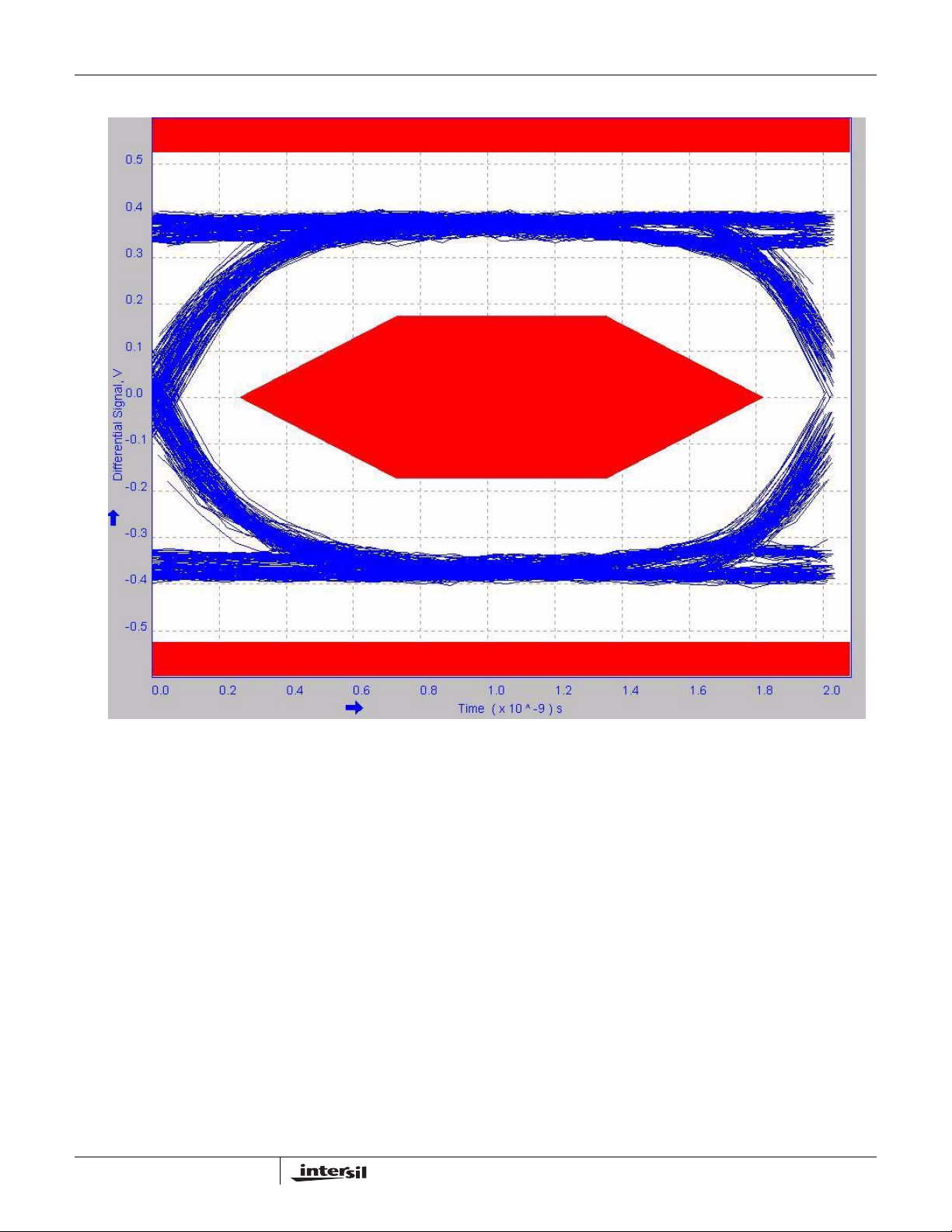
Typical Performance Curves T
VOLTAGE (835mV/DIV)
= +25°C, Unless Otherwise Specified (Continued)
A
VDD = 3.3V
TIME (0.2ns/DIV.)
FIGURE 9. EYE PATTERN WITH FAREND MASK: 480MBPS USB SIGNAL WITH HSX SWITCHES IN THE SIGNAL PATH
11
January 24, 2007
FN6408.0

ISL54200
Typical Performance Curves T
VOLTAGE (835mV/DIV)
= +25°C, Unless Otherwise Specified (Continued)
A
VDD = 3.3V
TIME (0.2ns/DIV.)
FIGURE 10. EYE PATTERN WITH NEAREND MASK: 480MBPS USB SIGNAL WITH HSX SWITCHES IN THE SIGNAL PATH
12
January 24, 2007
FN6408.0

ISL54200
Typical Performance Curves T
VOLTAGE (0.5V/DIV)
= +25°C, Unless Otherwise Specified (Continued)
A
VDD = 3.3V
FIGURE 11. EYE PATTERN: 12MBPS USB SIGNAL WITH HSX SWITCHES IN THE SIGNAL PATH
6
V+ = 3.3V
I
= 40mA
COM
5.5
85°C
5
(Ω)
4.5
(ON)
r
4
3.5
3
0 0.1 0.2 0.3 0.4
25°C
-40°C
V
COM
(V)
FIGURE 12. HSx SWITCH ON RESISTANCE vs SWITCH
VOLTAGE
13
TIME (0.2ns/DIV.)
-10
-20
-30
-40
-50
-60
-70
-80
NORMALIZED GAIN (dB)
-90
-110
RL = 45Ω
VIN = 0.2V
to 2V
P-P
P-P
0.01 0.1 1 500
FREQUENCY (MHz)
100.001 100
FIGURE 13. OFF-ISOLATION
FN6408.0
January 24, 2007

ISL54200
Typical Performance Curves T
-10
RL = 45Ω
-20
-30
-40
-50
-60
-70
-80
NORMALIZED GAIN (dB)
-90
-110
VIN = 0.2V
to 2V
P-P
P-P
0.01 0.1 1 500
FREQUENCY (MHz)
FIGURE 14. CROSSTALK
= +25°C, Unless Otherwise Specified (Continued)
A
Die Characteristics
SUBSTRATE POTENTIAL (POWERED UP):
GND (TDFN Paddle Connection: Tie to GND or Float)
TRANSISTOR COUNT:
98
PROCESS:
Submicron CMOS
100.001 100
14
FN6408.0
January 24, 2007

ISL54200
Ultra Thin Quad Flat No-Lead Plastic Package (UTQFN)
INDEX AREA
PIN #1 ID
NX (b)
5
SECTION "C-C"
6
N
2X
0.10 C
2X
0.10 C
0.10 C
0.05 C
SEATING PLANE
(DATUM A)
1
N
N-1
(A1)
D
21
TOP VIEW
A
A1
SIDE VIEW
2
e
3
(ND-1) X e
BOTTOM VIEW
NX L
(DATUM B)
NX b
0.10 M C A B
0.05 M C
C
L
e
CC
FOR ODD TERMINAL/SIDE
b
A
B
E
C
4xk
5
L
TERMINAL TIP
L10.2.1x1.6A
10 LEAD ULTRA THIN QUAD FLAT NO-LEAD PLASTIC
PACKAGE
MILLIMETERS
SYMBOL
A 0.45 0.50 0.55 A1 - - 0.05 A3 0.127 REF -
b 0.15 0.20 0.25 5
D 2.05 2.10 2.15 -
E 1.55 1.60 1.65 -
e 0.50 BSC -
k0.20
---
L 0.35 0.40 0.45 -
N102
Nd 4 3
Ne 1 3
θ
0-12
NOTES:
1. Dimensioning and tolerancing conform to ASME Y14.5-1994.
2. N is the number of terminals.
3. Nd and Ne refer to the number of terminals on D and E side,
respectively.
4. All dimensions are in millimeters. Angles are in degrees.
5. Dimension b applies to the metallized terminal and is measured
between 0.15mm and 0.30mm from the terminal tip.
6. The configuration of the pin #1 identifier is optional, but must be
located within the zone indicated. The pin #1 identi fier may be
either a mold or mark feature.
7. Maximum package warpage is 0.05mm.
8. Maximum allowable burrs is 0.076mm in all directions.
9. Same as JEDEC MO-255UABD except:
No lead-pull-back, "A" MIN dimension = 0.45 not 0.50mm
"L" MAX dimension = 0.45 not 0.42mm.
10. For additional information, to assist with the PCB Land Pattern
Design effort, see Intersil Technical Brief TB389.
NOTESMIN NOMINAL MAX
4
Rev. 3 6/06
0.10 MIN
0.05 MIN
DETAIL “A” PIN 1 ID
15
2.50
1.75
L
2.00
0.275
0.50
0.25
LAND PATTERN
0.80
10
FN6408.0
January 24, 2007

ISL54200
Thin Dual Flat No-Lead Plastic Package (TDFN)
(DAT UM B )
6
INDEX
AREA
(DATUM A)
NX (b)
5
SECTION "C-C"
6
INDEX
AREA
SEATING
PLANE
NX L
8
A
C
D
TOP VIEW
SIDE VIEW
D2
D2/2
12
N
N-1
e
(Nd-1)Xe
REF .
BOTTOM VIEW
(A1)
2X
A3
E2/2
NX b
5
C
L
e
CC
FOR ODD TERMINAL/SIDE
E
87
0.10
ABC0.10
2X
0.10
//
A
NX k
E2
M
TERMINAL TIP
0.10
0.08
L1
CB
BAC
L10.3x3A
10 LEAD THIN DUAL FLAT NO-LEAD PLASTIC PACKAGE
MILLIMETERS
SYMBOL
A
A1
A3
b
D
D2
E
C
C
E2
e
k
L
N
Nd
0.70 0.75 0.80
- - 0.05
0.20 REF
0.20 0.25 0.30
2.95 3.0 3.05
2.25 2.30 2.35
2.95 3.0 3.05
1.45 1.50 1.55
0.50 BSC
0.25 - -
0.25 0.30 0.35
10
5
NOTES:
1. Dimensioning and tolerancing conform to ASME Y14.5-1994.
2. N is the number of terminals.
3. Nd refers to the number of terminals on D.
4. All dimensions are in millimeters. Angles are in degrees.
5. Dimension b applies to the metallized terminal and is measured
between 0.15mm and 0.30mm from the terminal tip.
6. The configuration of the pin #1 identifier is optional, but must be
located within the zone indicated. The pin #1 identi fier may be
either a mold or mark feature.
7. Dimensions D2 and E2 are for the exposed pads which provide
improved electrical and thermal performance.
8. Nominal dimensions are provided to assist with PCB Land
Pattern Design efforts, see Intersil Technical Brief TB389.
9. Compliant to JEDEC MO-229-WEED-3 except for D2
dimensions.
L
9
NOTESMIN NOMINAL MAX
-
-
-
5, 8
-
7, 8
-
7, 8
-
8
2
3
Rev. 3 3/06
All Intersil U.S. products are manufactured, assembled and tested utilizing ISO9000 quality systems.
Intersil Corporation’s quality certifications can be viewed at www.intersil.com/design/quality
Intersil products are sold by description only. Intersil Corporation reserves the right to make changes in circuit design, software and/or specifications at any time without
notice. Accordingly, the reader is cautioned to verify that data sheets are current before placing orders. Information furnished by Intersil is believed to be accurate and
reliable. However, no responsibility is assumed by Intersil or its subsidiaries for its use; nor for any infringements of patents or other rights of third parties which may result
from its use. No license is granted by implicat ion or oth erwise u nde r any p a tent or p at ent r ights of Intersil or its subsidiaries.
For information regarding Intersil Corporation and its products, see www.intersil.com
16
FN6408.0
January 24, 2007
 Loading...