

Page 1
®
www.BDTIC.com/Intersil
ISL5416
Data Sheet August 2004
Four-Channel Wideband Programmable
DownConverter
The ISL5416 Four-Channel Wideband Programmable Digital
DownConverter (WPDC) is designed for high dynamic range
applications such as cellular basestations where the
processing of multiple channels is required in a small
physical space. The WPDC combines four channels in a
single package, each including: an NCO, a digital mixer,
digital filters, an AGC and a resampling filter.
All channels are independently programmable and may be
updated in real time. Each of the four channels can select
any of the four digital input buses. Each of the tuners can
process a W-CDMA channel. Channels may be cascaded or
polyphased for increased bandwidth. Selectable outputs
include I samples, Q samples, and AGC gain. Outputs from
the part are available over the parallel, serial or uP
interfaces.
Ordering Information
PART
NUMBER
ISL5416KI -40 to 85 256 BGA V256.17x17
ISL5416KIZ
(See Note)
ISL5416EVAL1 25 EVALUATION KIT
NOTE: Intersil Pb-free products employ special Pb-free material sets; molding
compounds/die attach materials and 100% matte tin plate termination finish, which is
compatible with both SnPb and Pb-free soldering operations. Intersil Pb-free
products are MSL classified at Pb-free peak reflow temperatures that meet or exceed
the Pb-free requirements of IPC/JEDEC J Std-020B.
TEMP
o
RANGE (
-40 to 85 256 BGA
C) PACKAGE PKG. DWG. #
(Pb-free)
V256.17x17
FN6006.3
Features
• Up to 95MSPS Input
• Four Parallel 16-bit Fixed or 17-bit Floating Point Inputs
• Programmable RF Attenuator/VGA Control
• 32-Bit Programmable Carrier NCO with > 110dB SFDR
• 20-bit Internal Data Path
• Filter Functions
- Multi-Stage Cascaded-Integrator-Comb (CIC) Filter
- Two programmable FIR Filters (first up to 32-taps,
second up to 64-taps)
- Half Band Interpolation Filter
- Resampling FIR Filter
• Overall decimation from 1 to >4096
• Digital AGC with up to 96dB of Gain Range
• Up to Four Independent 16-bit Parallel Outputs
• Serial Output Option
• 16-bit Pa rallel µP Interface
• 1.8V core, 3.3V I/O Operation
• Evaluation Board and Configuration Software available
• Pb-free available
Applications
• Basestation Receivers: GSM/EDGE, CDMA2000, UMTS.
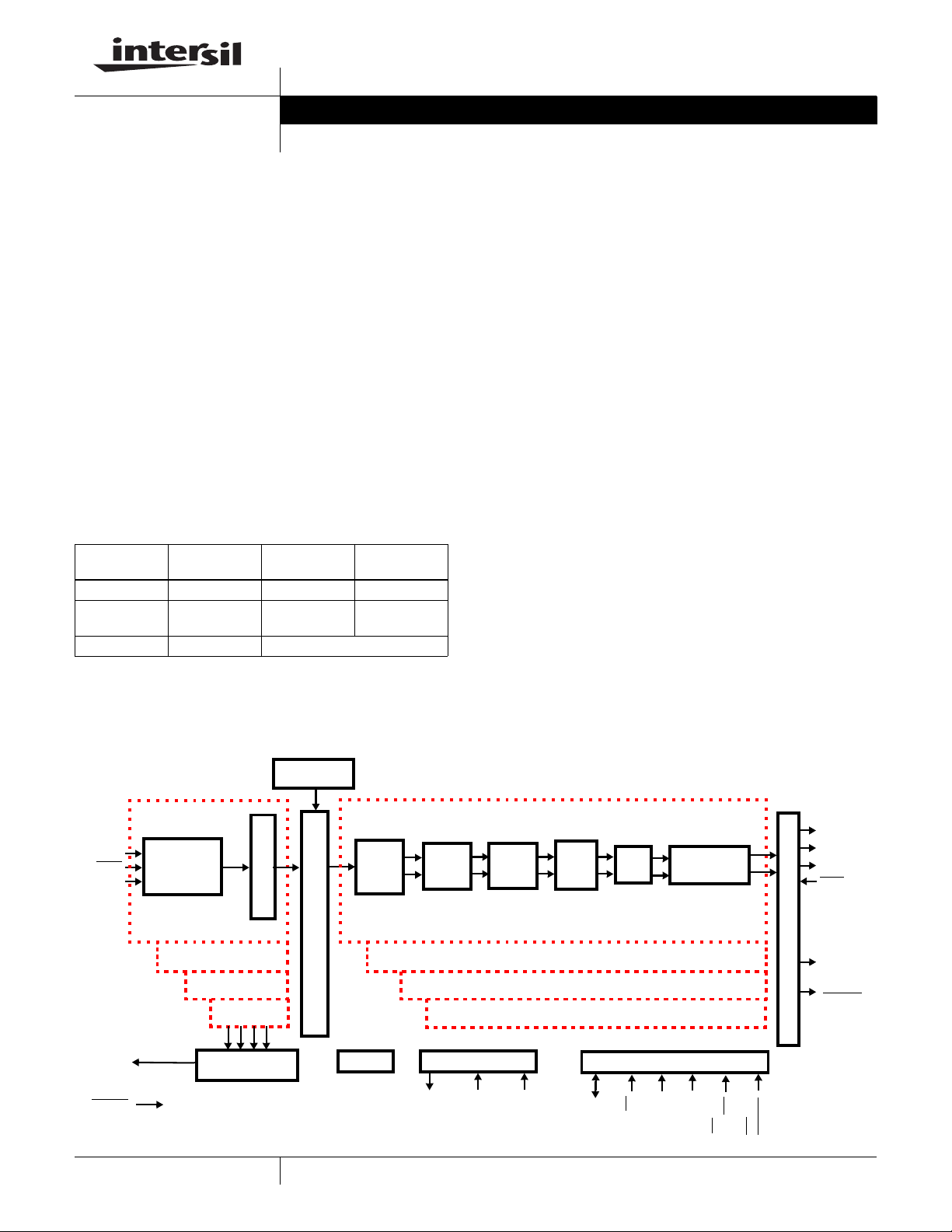
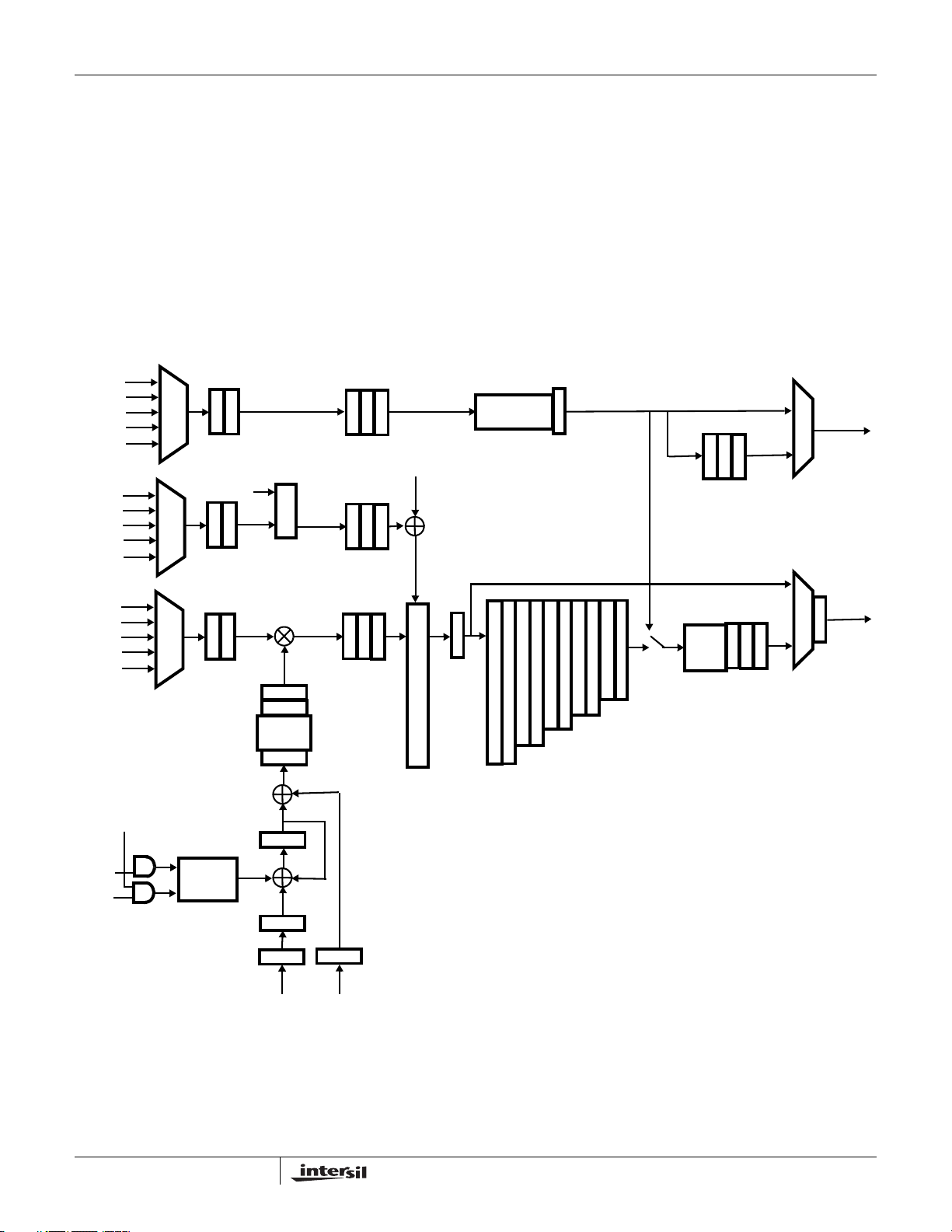
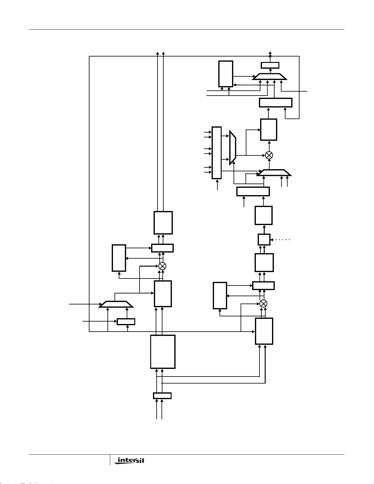
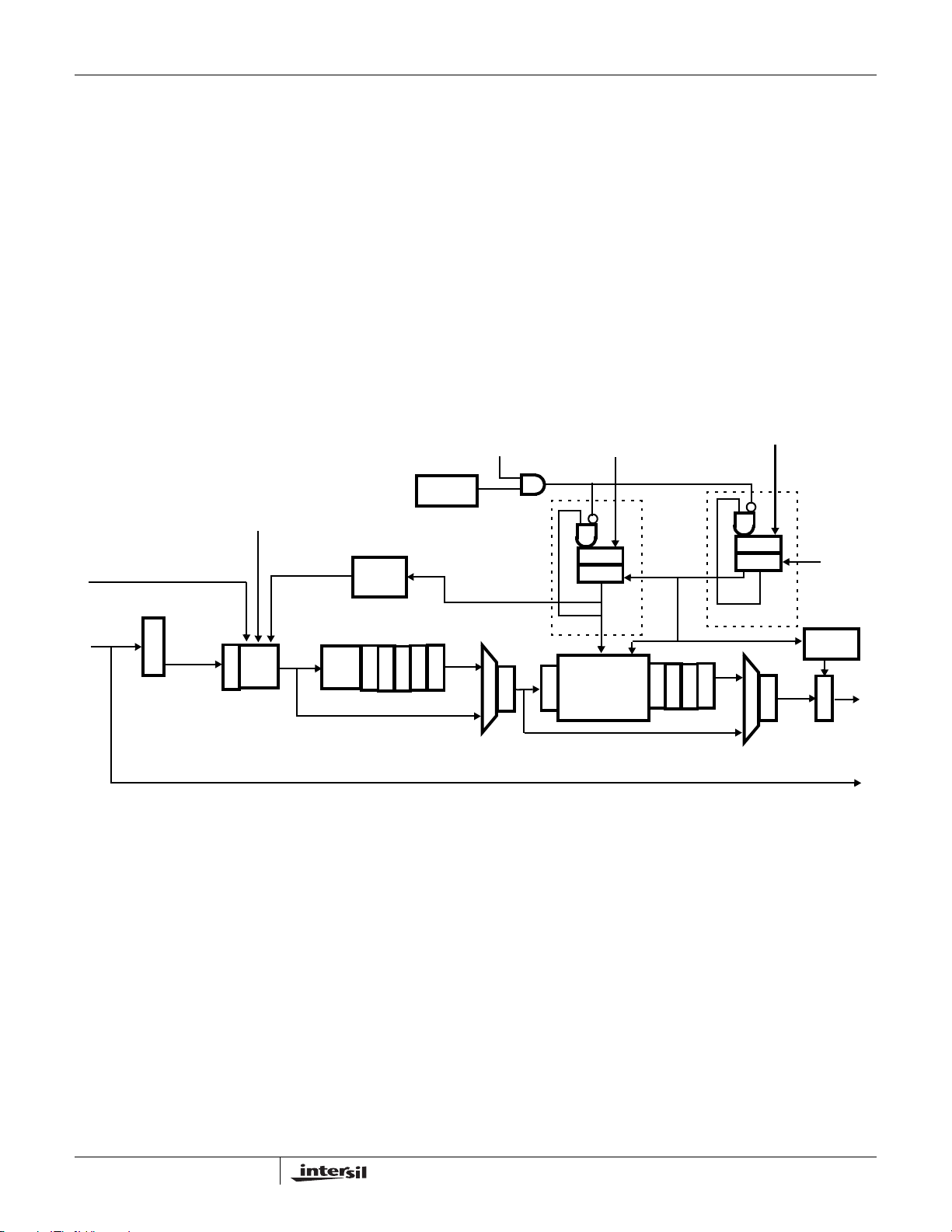
Block Diagram
TEST
REGISTER
AIN(16:0)
ENIA
CLKA
EOUT(15:0)
RESET
INPUT
SELECT
CLOCK &
FORMAT
RANGE CONTROL
INPUT A CHANNEL O
INPUT B
INPUT C
INPUT D
RF ATTENUATOR
VGA CONTROL
INPUT CHANNEL ROUTING
JTAG SYNCHRONIZATION
1
NCO
MIXER
CIC
I
Q
SYNCO SYNCIN1 SYNCIN2
1-888-INTERSIL or 321-724-7143
I
FIR1
FILTER
CAUTION: These devices are sensitive to electrostatic discharge; follow proper IC Handling Procedures.
Q
FILTER
FIR2
I
AGC
Q
| Intersil (and design) is a registered trademark of Intersil Americas Inc.
All other trademarks mentioned are the property of their respective owners.
OUTPUT
AOUT(15:8)
or
RD
RD/WR
I
Q
DSTRB
WR or
I
Q
P(15:0)
Copyright © Intersil Americas Inc. 2002-2004. All Rights Reserved
I
IHBF
µP INTERFACE
RESAMPLER
Q
CHANNEL 1
CHANNEL 2
CHANNEL 3
CE
ADD(2:0)
uP MODE
OUTPUT ROUTING & FORMATTING
AOUT(7:0)
FSYNCA
OEA
CLKO1
CLKO2
/INTRPT
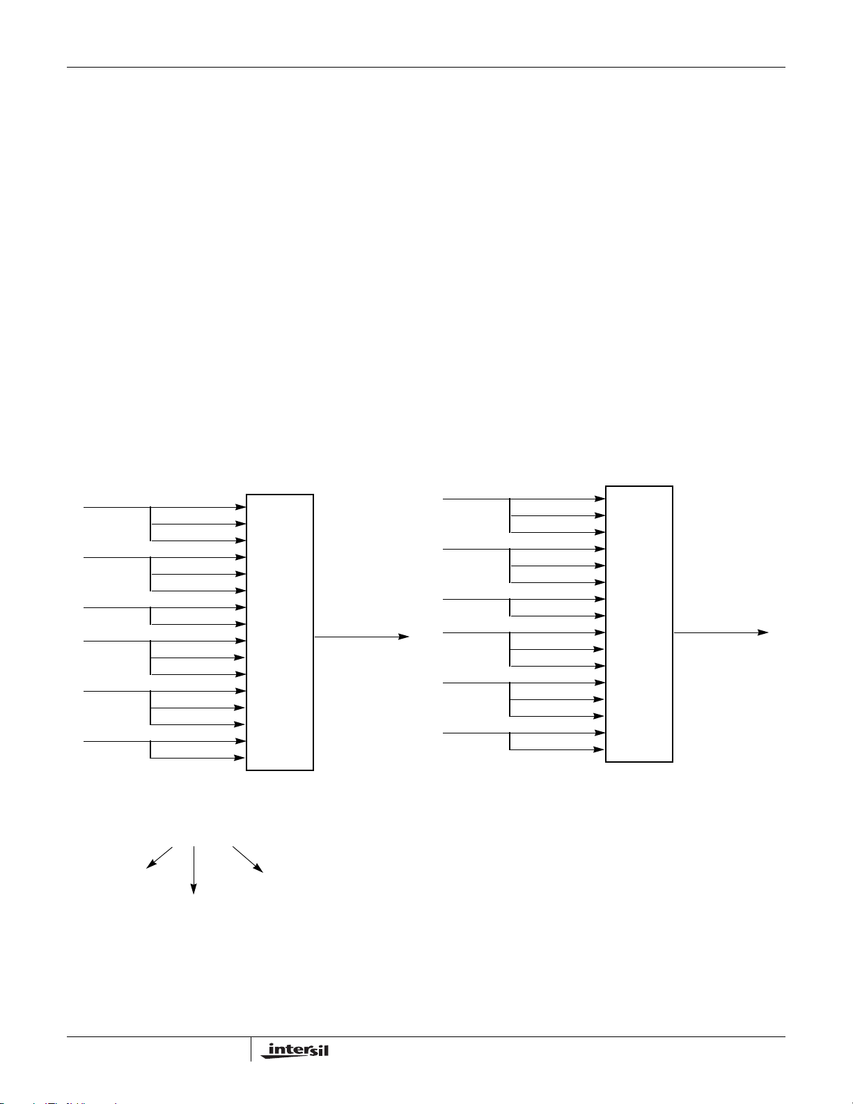
Page 2
TYPICAL CHANNEL
www.BDTIC.com/Intersil
FILTER
CASCADE
GAIN
ROUND
x1, 2, 4, 8
DIGITAL
TUNER
OUTPUT
20
/
FIR
20
2
/
1-64 TAPS
R=1-8
BYPASS
SATURATE
CHANNEL 0
24
/
AGC
24
/
OUTPUT
FORMAT
24
24
0 - 96 dB
BYPASS
R
16
O
/
/
/
U
16
/
N
D
CASCADE
AIN(16:0)
BIN(16:0)
CIN(16:0)
DIN(16:0)
TEST INPUT
2
DIGITAL
16
TUNING
/
MIXER
MUX
NCO
32-BIT CONTROL
>110 db SFDR
INPUT A
AIN(16:0)
ENIA
CLKA
INPUT
FORMAT
RANGE
CONTROL
INPUTS
CIC
24
/
FILTER
24
/
1-5 STAGES
R=2-64K
BYPASS
24
24
/
24
24
MUX
/
TEST
REGISTER
24
20
/
/
/
GAIN
FIR
24
20
1
/
/
/
1-32 TAPS
R=1-8
BYPASS
ROUND
x1, 2, 4, 8
SATURATE
CASCADE
IN
MUX
F
16
I
16
F
O
24
/
IHBF
/
24
/
/
16
/
RESAMPLING
16
FILTER
/
SLOT CONTROL
CH 0, 1 MUXING
TO PARALLEL
SEQUENCING
AND ROUTING
16
MUX
/
16
/
SELECT
FORMAT
TO SERIAL
TO uP
ROUTING
INTERFACE
AOUT(15:0)
FSYNCA
OEA
EXT AGC CNTRL
BIN(16:0)
ENIB
CLKB
INPUT B
INPUT
FORMAT
RANGE
CONTROL
CASCADE
OUT
MUX
DIGITAL
TUNER
CHANNEL 1
AGC GAIN
OUTPUT
FORMAT
MUX
SLOT CONTROL
CH 0, 1 MUXING
ISL5416
BOUT(15:0)
FSYNCB
OEB
CHANNEL 2
INPUT C
CIN(16:0)
ENIC
CLKC
INPUT
FORMAT
RANGE
CONTROL
MUX
DIGITAL
TUNER
OUTPUT
FORMAT
SLOT CONTROL
CH 2, 3 MUXING
O U T P U T M U L T I P L E X I N G
COUT(15:0)
FSYNCC
OEC
INPUT D
DIN(16:0)
ENID
CLKD
INPUT
FORMAT
RANGE
CONTROL
MUX
DIGITAL
TUNER
MUX
EOUT(15:0)
TRST
RESET
TMS
TCLK
TDI
TDO
JTAG
SYNCHRONIZATION
SYNCO
SYNCIN1
CHANNEL 3
AGC GAIN
SYNCIN2
OUTPUT
FORMAT
SEQUENCED uP READ DATA
uP INTERFACE
SLOT CONTROL
CH 2, 3 MUXING
SERIAL OUTPUTS
P(15:0), uPMODE, RD (RD/WR),
(DSTRB), CE, ADD(2:0)
WR
DOUT(15:0)
FSYNCD
OED
CLKO1
CLKO2/
INTRPT
Page 3
ISL5416
www.BDTIC.com/Intersil
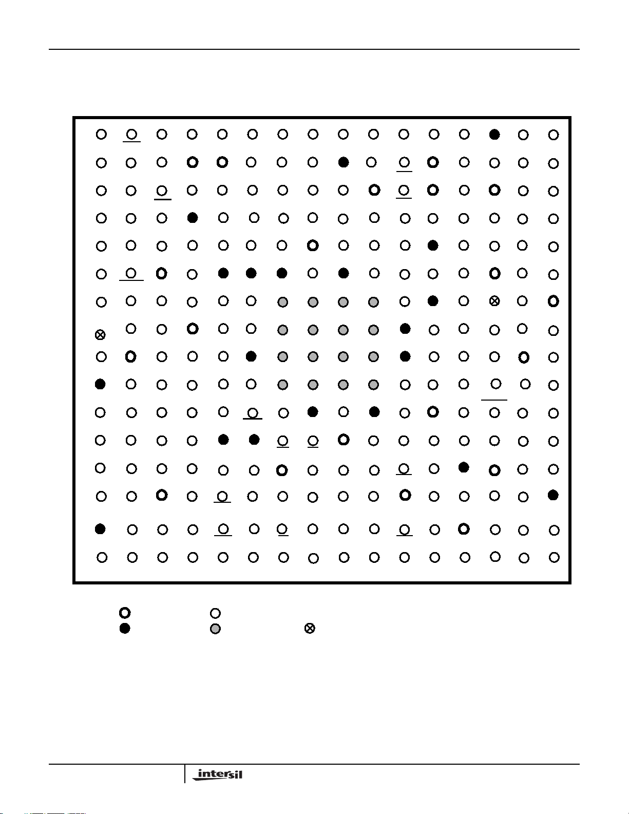
256-LEAD BGA
TOP VIEW
123456789 1110
A
Ain9
B
Ain8
C
Ain7
D
Ain6 Bout9
E
Ain5 Bout7Ain4
F
Ain3 Bout4 VccIORESET
G
Ain2 Bout3Ain1
H
J
CLKC
K
GND Dout15Cin16
L
Cin14 Dout14Cin15
M
Cin12
N
Cin10
P
Ain10 Ain11 Ain12 Ain14 Eout13
Bin9
Bin10
Bin8
ENIB
Bin7
Bin6 Bout8Bout14
Bin4
Vcc
Bin1 TMS TDI Aout3
Ain0
VccIO
Cin13
Cin11 Din10 Din11 Din4 Din3 Vcc
CLKD Eout6 Eout7 GND GND
Din16 P4
Eout3 Dout13Vcc
Din12 Din13 GND GND WR
Vcc Ain15Vcc
GND
Bin5 Eout10 Bin13 Eout11 Vcc P13 P11 TDO Aout6
Bin3
Bin2
Bin0
Eout4
Din15 Din14 GND Add1 GND
Bin14 Bin15 Eout14 P12
GND GND GND uPmode GND P10
Eout8 Eout9
Vcc
Eout5 Eout2 P3
Ain16
CLKB
Eout12
TRST Add2 P2
RD
Din0
Eout1
SYNCO Aout15SYNCIn1CLKA Aout14 Aout13 GNDENIA
SYNCIn2GNDEout15 Bout13
P15
VccIO OEB
P14
Dout0
Dout2 VccDout1Cin9
OEA
Bout15
GND
P0 Dout3Vcc
P1 OED
12
Vcc
VccIO FSYNCBBin11 Bin12 Ain13 Bin16
P9
Bout5
P8
GND
P7
Add0 Dout11 Dout12
Dout4
Dout5 Dout6 Dout7Din9 Vcc Din6 ENID Din2 Din1
13
14
Bout12
VccIO
Bout6GND
Bout1 Bout2
P6P5
Bout0
CLKO2/
INTRPT
GND VccIO
15 16
Aout12 Aout11
Bout11
FSYNCA
Aout10
Bout10
Aout8
Aout4 Aout5
Aout1 Aout2
CLKO1 Cout15
Cout14
Cout12 Cout11
Dout10 Cout10
Dout9
VccIO
Aout9
Aout7
Vcc
Aout0
Cout13
GND
R
GND
T
POWER PIN
GROUND PIN
Vcc = +1.8V CORE SUPPLY VOLTAGE
VccIO = +3.3V I/O SUPPLY VOLTAGE
NOTE: Thermal Balls should be connected to the ground plane
Unused Input Balls should be connected to ground or V
SIGNAL PIN
THERMAL BALL
Eout0
IO as appropriate
cc
Cin0
NC (NO CONNECTION)
Cout2 OECCout0
TCLK Cout3Cout1Cin8
3
Cout4Din8 Din7 Din5 ENIC Cin2 CE
Cout5 Cout6 FSYNCCCin7 Cin6 Cin5 Cin4 Cin3 Cin1
VccIO FSYNCD
Dout8 Cout9
Cout7
Cout8
Page 4
ISL5416
www.BDTIC.com/Intersil
Pin Descriptions
INTERNAL
NAME TYPE
POWER SUPPLY
Vcc - Positive Power Supply Voltage (core), 1.8V ±0.09
VccIO - Positive Power Supply Voltage (I/O), 3.3V ±0.165
GND - Ground, 0V.
INPUTS
PULL-UP/DOWN DESCRIPTION
Ain(16:0) I PULL DOWN Parallel Data Input bus A. Sampled on the rising or falling edge (programmable) of clock when ENIA
Bin(16:0) I PULL DOWN Parallel Data Input bus B. Sampled on the rising or falling edge (programmable) of clock when ENIB
Cin(16:0) I PULL DOWN Parallel Data Input bus C. Sampled on the rising or falling edge (programmable) of cloc k when ENIC
Din(16:0) I PULL DOWN Parallel Data Input bus D . Sampled on the rising or falling edge (prog r ammab le) of cloc k when ENID
ENIA
ENIB
ENIC
ENID
CONTROL
CLKA I PULL DOWN Input clock for data bus A. CLKA or CLKC may be used for Ain(16:0).
I PULL DOWN Input enable for Parallel Data Input bus A. Active low. This pin enables the input to the part in one of
I PULL DOWN Input enable for Parallel Data Input bus B. Active low. This pin enables the input to the part in one of
I PULL DOWN Input enable for Parallel Data Input bus C. Active low. This pin enables the input to the part in one of
I PULL DOWN Input enable for Parallel Data Input bus D. Active low. This pin enables the input to the part in one of
is active (low). The bus order can be programmed (See IWA = 0*00h, bit 4).
is active (low). The bus order can be programmed (See IWA = 0*00h, bit 4).
is active (low). The bus order can be programmed (See IWA = 0*00h, bit 4).
is active (low). The bus order can be programmed (See IWA = 0*00h, bit 4).
two modes, gated or interpolated. In gated mode, one sample is taken per CLK when ENIx
asserted.
two modes, gated or interpolated. In gated mode, one sample is taken per CLK when ENIx
asserted.
two modes, gated or interpolated. In gated mode, one sample is taken per CLK when ENIx
asserted.
two modes, gated or interpolated. In gated mode, one sample is taken per CLK when ENIx
asserted.
is
is
is
is
CLKB I PULL DOWN Input clock for data bus B. CLKB or CLKC may be used for Bin(16:0).
CLKC I Input clock for data bus C. CLKC is also the master clock for all channels of ISL5416
CLKD I PULL DOWN Input clock for data bus D. CLKD or CLKC may be used for Din(16:0).
SYNCIn1 I PULL DOWN Global synchronization input signal 1. SYNCIn1 can update the carrier NCOs, reset decimation
counters, restart the filter, and restart the output section among other funct ions. For most of the
functional blocks, the response to SYNCIn1 is programmable and can be enabled or disabled.
SYNCIn2 I PULL DOWN Global synchronization input signal 2. SYNCIn2 can update the carrier NCOs, reset decimation
counters, restart the filter, and restart the output section among other funct ions. For most of the
functional blocks, the response to SYNCIn2 is programmable and can be enabled or disabled.
SYNCO O Synchronization Output Signal. The processing of multiple ISL5416 devices can be synchronized by
RESET
I PULL UP Reset Signal. Active low. Asser ting reset will halt all processing and set cer tain registers to default
tying the SYNCO from one ISL5416 device (the master) to the SYNCIn of all the ISL5416 devices
(the master and slaves). An optional internal SYNCO to SYNCInX connection is provided.
values.
4
Page 5
Pin Descriptions (Continued)
www.BDTIC.com/Intersil
ISL5416
NAME TYPE
JTAG
TDO O Test data out
TDI I PULL UP Test data in.
TMS I PULL UP Test mode select.
TCLK I PULL DOWN Test clock.
TRST
OUTPUTS
Aout(15:0) O Parallel Data Output bus A. A 16-bit parallel data output which can be programmed to consist of I, Q,
Bout(15:0) O Parallel Data Output bus B. A 16-bit parallel data output which can be programmed to consist of I, Q,
I PULL UP Test reset. Active low. If JTAG not used, tie this pin low. If there is a trace connected to the pin and
INTERNAL
PULL-UP/DOWN DESCRIPTION
there is enough board noise, the JTAG port might get into an unexpected state and stop
communications with the part
AGC. Data from Channels 0, 1, 2 and 3 can be multiplexed into a common parallel output data bus.
Information can be sequenced in a programmable order. Can be ones complemented. Can be
divided into two 8-bit busses. See Data Output Formatter Section and Microprocessor Interface
Section. See Table 24.
AGC. Data from Channels 0, 1, 2 and 3 can be multiplexed into a common parallel output data bus.
Information can be sequenced in a programmable order. Can be ones complemented. Can be
divided into two 8-bit busses. See Data Output Formatter Section and Microprocessor Interface
Section.
Cout(15:0) O Parallel Data Output bus C . A 16-bit parallel data output which can be programmed to consist of I, Q,
AGC. Data from Channels 0, 1, 2 and 3 can be multiplexed into a common parallel output data bus.
Information can be sequenced in a programmable order. Can be ones complemented. Can be
divided into two 8-bit busses. See Data Output Formatter Section and Microprocessor Interface
Section.
Dout(15:0) O Parallel Data Output bus D. A 16-bit parallel data output which can be programmed to consist of I, Q,
AGC. Data from Channels 0, 1, 2 and 3 can be multiplexed into a common parallel output data bus.
Information can be sequenced in a programmable order. Can be ones complemented. Can be
divided into two 8-bit busses. See Data Output Formatter Section and Microprocessor Interface
Section.
Below is the table of the serial output bits allocation for DOUT.
SERIAL OUTPUT BITS ALLOCATION
SER. OUTPUT A SER. OUTPUT B SER. OUTPUT C SER. OUTPUT D
SCLKX * DOUT0 DOUT4 DOUT8 DOUT12
SSYNCX * DOUT1 DOUT5 DOUT9 DOUT13
SD1X * DOUT2 DOUT6 DOUT10 DOUT14
SD2X * DOUT3 DOUT7 DOUT11 DOUT15
X denotes A, B, C, D as appropriate
*
Eout(15:0) O A 16-bit parallel VGA/Attenuator control output. Partitionable into separate 4 or 8-bit busses.
CLKO1 O Output Clock 1. Can be programmed to be at CLKC/N for N = 1 to 16. The polarity of CLKO1 is
programmable.
CLKO2/
INTRPT
O Available ONLY on Rev B (final) version of the part. Provides a complementary output or a second
clock to simplify board routing. Polarity is programmable. It can also be programmed as an interrupt
from one or more channels for a sequenced read (FIFO-like) mode. See register GWA = 0000h, bit
13.
5
Page 6
Pin Descriptions (Continued)
www.BDTIC.com/Intersil
ISL5416
NAME TYPE
FSYNCA O Frame Synchronization output signal for bus Aout(15:0).
FSYNCB O Frame Synchronization output signal for bus Bout(15:0).
FSYNCC O Frame Synchronization output signal for bus Cout(15:0).
FSYNCD O Frame Synchronization output signal for bus Dout(15:0).
OEA
OEB
OEC
OED
MICROPROCESSOR INTERFACE
P(15:0) I/O Microprocessor Interface Data bus. See Microprocessor Interface Section. P15 is the MSB.
ADD(2:0) I Microprocessor Interface Address bus. ADD2 is the MSB. See Microprocessor Interface Section.
WR
or
DSTRB
I PULL UP Output three-state enable for Parallel Data Output bus A. Active low.
I PULL UP Output three-state enable for Parallel Data Output bus B. Active low.
I PULL UP Output three-state enable for Parallel Data Output bus C. Active low.
I PULL UP Output three-state enable for Parallel Data Output bus D. Active low.
I Microprocessor Interface Write or Data Strobe Signal. When the Microprocessor Interface Mode
INTERNAL
PULL-UP/DOWN DESCRIPTION
Control (µP MODE) is low, data transf ers (from P(15:0) to the internal write holding register) occur on
the low to high transition of WR
input functions as a data strobe DSTRB
P(15:0) to the internal write holding register) occur on the low to high transition of DSTR B
high the data from the address specified is placed on P(15:0) when DSTRB is low. See the
RD/WR
Microprocessor Interface Section.
when CE is asserted (low). When the µP MODE control is high this
control. In this mode with RD/WR low, data transfers (from
. With
RD
or
RD/WR
µP MODE I PULL DOWN Microprocessor Interface Mode Control. This pin is used to select the Read/Write mode for the
CE
I Microprocessor Interfa ce Read or Read/Write Signal. When the Microprocessor Interface Mode
I Microprocessor Interface Chip Select. Active low. This pin has the same timing requirements as the
Control (µP MODE) is low, the data from the address specified is placed on P(15:0) when RD
asserted (low) and CE
a Read/Write
appropriate register when low. See the Microprocessor Interface Section.
Microprocessor Interface. When 0, RD
is 0, the microprocessor interface consists of separate RD
interface consists of a RD/WR
Section.
address pins.
control input. Data is read from P(15:0) when RD/WR high or written to the
is asserted (low). When the µP MODE control is high this input functions as
and WR, when 1, DSTROBE and RD/WR. When µP MODE
and WR strobes; when µP MODE is 1, the
control and a single data strobe. See the Microprocessor Interface
is
6
Page 7

ISL5416
www.BDTIC.com/Intersil
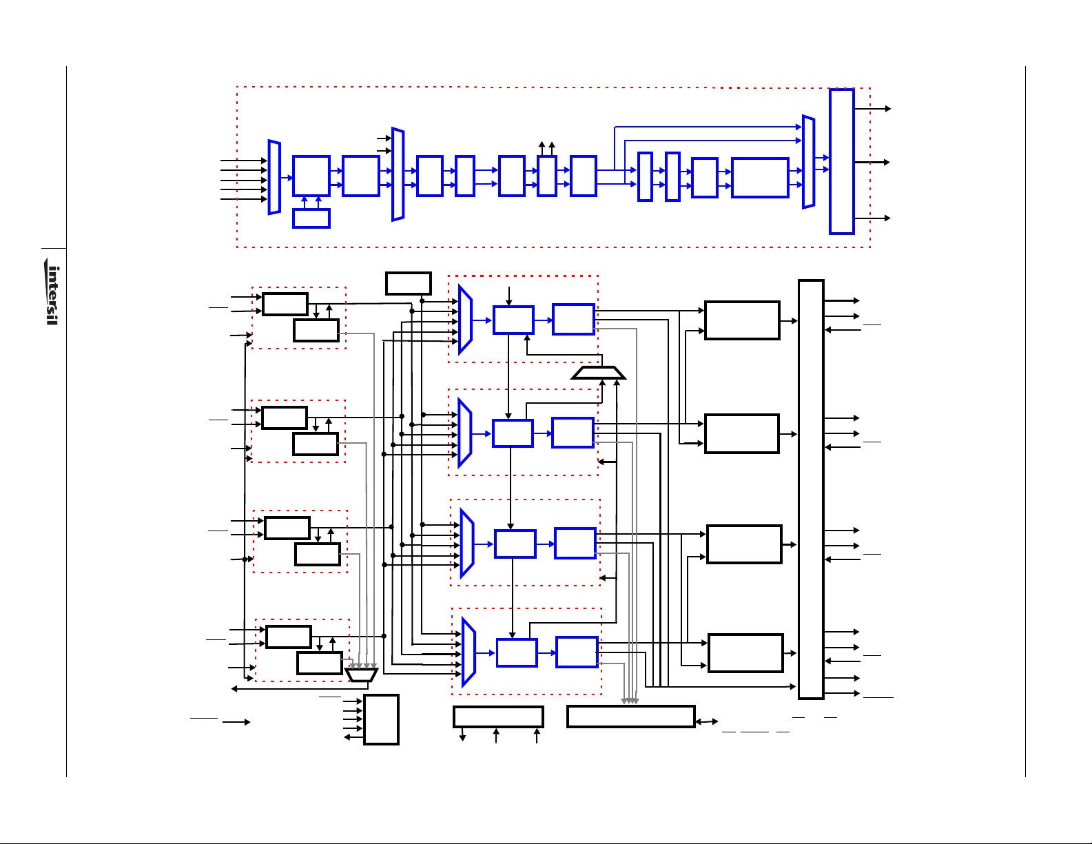
Functional Description
The ISL5416 is a four channel digital receiver integrated
circuit offering exceptional dynamic range and flexibility.
Each of the four channels consists of a front-end NCO,
digital mixer, CIC-filter, two FIR filters, AGC, Interpolation
Half Band Filter and Re-sampling Filter. The parameters for
the four channels are independently programmable.
There are four 17-bit parallel data input busses (Ain(16:0),
Bin(16:0), Cin(16:0) and Din(16:0)). The ISL5416 supports
both fixed and floating point parallel data input modes. The
floating point modes support gain ranging A/D converters or
A/D converter and RF/IF Attenuators or VGAs. Gated or
interpolated data input modes are supported. Each input can
be connected to any or all of the internal signal processing
channels, Channels 0, 1, 2 and 3. The four channels share a
common processing clock (CLKC). Four input clocks are
provided to allow for clock skew between input sources.
Each input has a Range Control circuits to monitor the signal
level on the parallel data busses and to control the gain prior
to the A/D converters. A 16-bit bus (Eout(15:0)) is provided
to control the external VGA/RF Attenuators.
Each front end NCO/digital mixer/CIC filter section incl udes a
quadrature numerically controlled oscillator (NCO), digital
mixer , barrel shifter and a casca ded-integ r ator-comb filter
(CIC). The NCO has a 32-bit frequency control word. The
SFDR of the NCO is >110dB. The barrel shifter provides a
gain of between 2
CIC. The CIC filter order is programmable from 1 to 5 and the
CIC decimation factor can be programmed from 2 to 512 for
th
5
order, 2048 for 4th order, 32768 for 3rd order, or 65536 for
st
1
or 2nd order filters. The CIC filter can also be bypassed.
Each channel back end section includes two FIR filters, an
AGC, Interpolation Half Band Filter and Resampler. The first
FIR filter can have up to 32 taps and the second can have up
to 64 taps. The 32-tap filte r calculates 4 taps per clock, while
the 64-tap filter calculates 8 taps per clock. The coefficients
for the programmable digital filters are 20 bits wide. Each
FIR filter can be bypassed. The AGC section can provide up
to 96dB of either fixed or automatic gain control. For
automatic gain control, two settling modes and two sets of
loop gains are provided. Separate attack and decay slew
rates are provided for each loop gain. Programmable limits
allow the user to specify a gain range less than 96dB.
A fixed coefficient interpolate-by-2 Half Band Filter and a
non-integer resampling filter follow the AGC. Coefficients for
the resampling filter are provided in ROM.
Four 16-bit parallel data outputs (Aout(15:0), Bout(15:0),
Cout(15:0) and Dout(15:0)) are provided. The output of each
channel can be routed to any of the output buses. Outputs
from more than one channel can be multiplexed through a
common output if the channels are synchronized.
Dout(15:0)) can alternately be used as four serial output
pairs. A common output clock (CLKO1) is used for the
-45
and 4 to compensate for the gain in the
parallel output buses. A second clock output pin
(CLKO2/INTRPT
allow a complementary output clocks.
The ISL5416 is programmed through a 16-bit
microprocessor interface. The output data can also be read
via the microprocessor interface. The ISL5416 is specified to
operate to a maximum clock rate of 95 MSPS over the
industrial temperature range (-40
supply voltage range is 3.3V ± 0.165V while the core power
supply voltage is 1.8V ± 0.09V.
) is provided to simplify board routing or to
o
C to 85oC). The I/O power
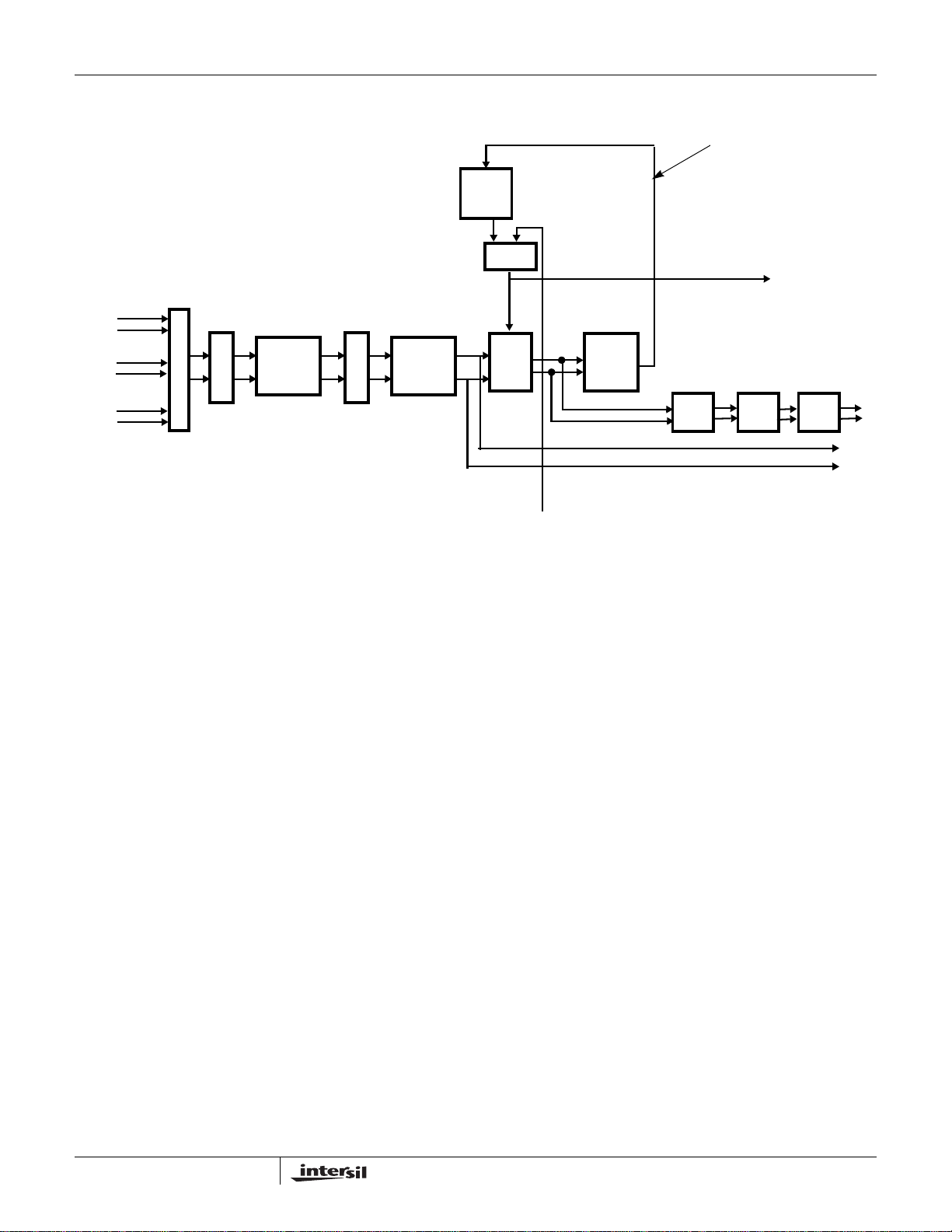
Input Select/Format Block
CLOCKING
The channel processing and output timing is clocked with the
rising edge of CLKC. Each input bus can be cloc ked with the
rising or falling edge of its o wn cloc k or with the rising or f alling
edge of CLKC. The frequency of all the cloc ks m ust be the
same, but providing separate clocks allows the inputs from
multiple A/D converters to have a small amount of ske w.
INPUT FORMAT
The inputs can be fixed point or floating point with
mantissa/exponents sizes of 14/3, 15/2, or 16/1. The
exponent inputs are added to the exponent from the internal
range control circuits, so if the range control circuits are
used, the exponent pins are typically grounded and/or
disabled via software in IWA = 0*10h, bit 3. The input format
may be twos complement or offset binary format in either
fixed or floating point modes (IWA = 0*00h).
GATED/INTERPOLATED MODES
For input sample rates at sub-multiples of the clock rate,
gated and interpolated input modes are provided. Each input
channel has an input enable (ENIx
gated mode, one input sample is processed per clock that
the ENIx
when ENIx
part to minimize delay (latency). In the interpolated mode,
the input is zeroed when the ENIx
processing inside the part continues. This mode inserts
zeros between the data samples, interpolating the input data
stream up to the clock rate. The spacing between ENIx
signals must be constant in the interpolated mode.
MULTIPLEXED INPUT MODE
Each input section can select one channel from a
multiplexed data stream of up to 8 channels. The input
enable is delay ed by 0 to 7 cloc k cycles to enab le a selection
register. The register following the selection register is
enabled by the non-delayed input enable to realign the
processing of the channels. The one-clock-wide input enable
must align with the data for the first channel. The desired
channel is then selected by programming the delay. A delay
of zero selects the first channel, a delay of 1 selects the
second, etc. Each input section selects only one channel of
the multiplexed stream, so a separate input bus must be
used for each channel of the multiplexed data stream.
signal is asserted (low). Processing is disabled
is high. The ENIx signal is pipelined through the
, x = A, B, C or D). In the
signal is high, but
7
Page 8
CLKC
www.BDTIC.com/Intersil
CLKX
CLKC
CLKX
ISL5416
R1 R2 R3 R4
R1 R2 R3 R4
INTERPOLATE
BUS REVERSE
R1
ENIX
XIN(16:0)
R
R
E
G
^
CLK/CLK
CLKX/CLKC
CLKX
CLKC
NOTE: To simplify the board routing, each of the four input data busses can be reversed, MSB for LSB (see IWA = 0*00h, bit 4)
M U X
R2
R
E
G
^
M U X
R3 R4
R
R
E
E
G
G
^
(16:0)
M
^
U
(0:16)
X
FIGURE 1. INPUT SECTION
OBIN
F
M
T
FLOAT/FIX
SLOT#
R
M
A
P
R
D
E
M
G
U
X
^
MANTISSA
EXPONENT
DIN (ONLY)
PROCESSING
ENABLE
TO CHANNELS
AND RANGE
CONTROL
TO SE RIAL
FREQUENCY
OFFSET
CLK
SYNCInX Use
SYNCInX main purpose is as a processing start-up signal
after a reset to align the start of processing of multiple
channels or chips. This assures that the carrier phases have
a known relationship and that the output timing aligns for
multiplexing outputs. It can also be used after start-up as a
system timing synchronization signal. Two SYNCInX signals
are provided so that one can be used as a regularly
occurring signal (such as at time slot boundaries) and one
as an infrequent signal (such as at start up or at 1 pps). If
more than one air interface standard is processing in one
part, one SYNCInX signal could be used for the slot timing
for each standard.
8
Register updates from a processor write are synchronized to
the clock, so that the register updates in multiple channels of
the same part are time aligned. However, when
synchronizing multiple parts the processor will need
knowledge of the SYNCInX timing so that enabling the
SYNCInX in multiple parts occurs between SYNCInX pulses.
Alternatively, SYNCIn1 could be used as a regularly
occurring SYNCI signal and SYNCIn2 could be a gated
version. The channel processing control register might only
be updated on SYNCIn2 and the other SYNCI functions
would respond to SYNCIn1.
Page 9

ISL5416
www.BDTIC.com/Intersil
VGA/RF Attenuator (A/D Range Control)
The range control section monitors the output of the A/D and
adjusts the RF/IF gain to maintain a desired A/D output
range. The gain adjustments are in 6 dB steps. The levels,
adjustment rates, and gain to bit mapping are
programmable.
The range control section uses three programmable
thresholds. Two thresholds, an upper and a lower threshold,
are compared against the average magnitude of the A/D
output. The range control adjusts the gain to keep the
average A/D output between the upper and lower thresholds.
If the average is above the upper threshol d, an internal
attenuator control register is increased by a programmable
amount. If the average is below the lower threshold, the gain
attenuator control register is decreased by a separate
programmed amount. The number of samples averaged for
each decision is programmable. The adjustments to the
attenuator control register can be less than 6 dB to further
filter the inputs. Only the three MSBs of the attenuator
control register are used to control the RF/IF gain, and these
are weighted as 6, 12, 24 dB steps.
The third threshold, an immediate threshold, is compared
against the magnitude of each A/D sample. If the magnitude
of any A/D sample exceeds the threshold, the attenuator
control register is immediately increased by the amount
programmed for the immediate threshold. Because there will
be some time delay from a regist er chan ge unt il the ef fect of
the change is seen at the A/D, the immediate threshold is
disabled for a programmable number of clock cycles after it
has been triggered.
To maximize the input sensitivity the range control also
includes a programmable bias. If the average signal is
between the upper and lower threshold, the bias value is
added from the attenuator control register. This bias
removes attenuation when it is no longer needed to avoid
missing small signals due to high input noise figure.
Four counters control the amount of time that the input is
averaged and align the adjustments to time slot boundaries.
One counts out the time slot period. If desired, this counter
can be reset by a SYNCInX signal to align its count to the
system timing. A second counter provides a programmable
delay from the start of the first counter's period to the start of
the integration period. This compensates for system delays
or allows the adjustments to be made over a certain portion
of the time slot. The third counter sets the integration period
for averaging the input samples for the upper and lower
threshold decisions. The fourth counter controls the number
of integration periods per time slot. See Figure 2 for a block
diagram. Note that the counters are ignored for the
immediate threshold decisions.
The user can program a separate code for output on the
EOUT bus for each of the eight possible states of the three
MSBs of the attenuator control register. These codes can be
up to 8 bits, but if four gain control sections are used, only
four bits are available for each gain control section. The
mapping of the gain control bits to EOUT bits is done in
GWA = 0001h and the codes are programmed in IWA =
0*17h and 0*18h.
The three MSBs of the attenuator control register can be
routed internally to the channels to be used as the floatingpoint exponents. This adds gain in 6 dB steps to compensate
for the 6 dB steps of RF attenuator. The MSBs can be added
to the input exponent bits if desired. There is a
programmable delay from the attenuator control register to
the channel input to compensate for RF/IF filter group delay
and A/D and ISL5416 pipeline delays.
9
Page 10
ISL5416
www.BDTIC.com/Intersil
SYNC
INTERVAL
(SLOT
PERIOD)
DELAY
(SYNC TO
START OF
INTEGRATION)
INTEGRATION
TIME
INTEGRATIONS
PER SLOT - 1
LD
DOWN
COUNTER
LD
DOWN
COUNTER
LD
DOWN
COUNTER
EN
LD
DOWN
COUNTER
EN
EN
=0
≥0
=0
<0
=0
≥0
ENABLE COUNTERS
ENABLE
UPDATES
B
TH1
FROM INPUT SECTION
MANTISSA
|X|
BYPASS
BW SELECT
REG
DUMP
(-1 TO -16)
2
TH2
B
A
∆
∆
B
A
HPF
|X|
Σ
REG
BARREL
SHIFT
TH3
A
∆
EXPONENT
EN
INPUT
EXP
Σ
EN
ATTEN
EXP
1-256
CLOCKS
PROG
DELAY
CIC SHIFT VALUE
OFFSET TO BASE
EOUT
16
A<B
LOWER
LIMIT
DETECTOR
MUX
R
E
G
3
LUT
PRLD(7:0)
LD
DOWN
COUNTER
µP ENABLE
“0”
BIAS
DELTA1
DELTA2
DELTA3
A>B
IMMEDIATE
MUX
REG
DECODE
Σ
A>B
UPPER
8
R
E
MAP
G
8
8
8
FROM
OTHER
DETECT.
UPPER GAIN LIMIT
LOWER GAIN LIMIT
8
LUT = LOOK UP TABLE
FIGURE 2. RANGE CONTROL BLOCK DIAGRAM
10
Page 11
A
ISL5416
www.BDTIC.com/Intersil
NCO/Mixer
After the input select/format section, the samples are
multiplied by quadrature sine wave samples from the carrier
NCO. The NCO has a 32-bit frequency control, providing
sub-hertz resolution at the maximum clock rate. The
quadrature sinusoids have exceptional purity. The purity of
the NCO should not be the determining factor for the
receiver dynamic range performance (A typical spectrum
plot is shown in Figure 20). The phase quantization to the
sine/cosine generator is 24 bits and the amplitude
quantization is 19 bits.
ENA
ENB
ENC
END
ENµP
EXPA
EXPB
EXPC
EXPD
EXPµP
MUX
MUX
R
R
E
E
G
G
MAX EXP
R
R
E
E
G
G
R
R
R
E
E
E
G
G
G
BASE
SHIFT
C
L
I
P
R
R
E
E
G
G
VALUE
(from uP)
R
E
G
The carrier NCO center frequency is loaded via the uP bus. The
center frequency control is double buffered -- the input is loaded
into a holding register via the uP interface. The data is then
transferred from the holding register to the active register by a
write to a special address or by a SYNCInX signal, if enabled in
IWA = *000h. To synchronize multiple channels, the carrier
NCO phase accumulator feedback can be zeroed on loading to
restart all of the NCOs at the same phase (see IWA = *005h).
The phase of the NCO can be offset by programming IWA =
*003h. The phase offset is not double buffered.
DECIMATION
COUNTER
0...-23
R
E
G
R
R
R
E
E
E
G
G
G
MUX
MUX
R
E
G
MANT
BMANT
CMANT
DMANT
PMANT
(TEST INPUT)
ENCOF
COF
COFSYNC
MUX
SERIAL
FREQ
OFFSET
0...-15 0...-23
R
R
E
E
G
G
REG
REG
SIN/COS
GEN
REG
REG
REG
0...-18
0...-23
R
R
R
E
E
E
G
G
G
-45
47
TO 2
0
FIXED INPUT GAIN = 2
SHIFT GAIN = 2
R
E
G
REG
REG
INTEGRATE
INTEGRATE
REG
INTEGRATE
REG
INTEGRATE
INTEGRATE
BARREL SHIFTER
69b
53b
62b
34b
44b
CIC ORDER FIR COEFFICIENTS
11-1
21-21
REG
0...-29
FIR
FILTER
(COMB)
0...-23
R
R
R
E
E
E
G
G
G
31-33-1
REG
REG
41-46-41
5 1 -5 10 -10 5 -1
CENTER
FREQ
PHASE
OFFSET
NOTE:
BUS NUMBERING SUCH AS 0...-23 INDICATES BIT WEIGHTS
SUCH AS 2
0
... 2
-23
FIGURE 3. NCO, MIXER AND CIC BLOCK DIAGRAM
11
Page 12

ISL5416
www.BDTIC.com/Intersil
TABLE 1. PN GENERATOR BIT WEIGHTING
2^
SIGNAL 0 -1 -2 -3 -4 -5 -6 -7 -8 -9 -10 -11 -12 -13 -14 -15 -16 -17 -18 -19 -20 -21 -22 -23
PN SSSXXXXXXXXXXXXXXXX
GAIN REG XXXXXXXXXXXXXXXX
PN Generator
After the mixers, a PN (pseudonoise) signal can be added to
the data. This feature is provided for test and to digitally reduce
the input sensitivity and adjust the receiver range (sensitivity).
The effect is the same as increasing the noise figure of the
receiver, reducing its sensitivity and overall dynamic range.
The one bit PN data is scaled by a 16 bit programmable
scale factor. The overall range fo r the PN is 0 to 1/4 full
scale. A gain of 0 disables the PN input. The bit weighting for
the gain is shown in table 1.
The minimum, non-zero, PN value is 1/2
dBFS) on each axis (-105 dbFS total).
18
of full scale (-108
CIC Filter
Next, the signal is filtered by a cascaded integrator/comb
(CIC) filter. A CIC filter is an efficient architecture for
decimation filtering. The power or magnitude squared
frequency response of the CIC filter is given by:
------------------------
Pf()
=
sin
where
M = Number of delays (1 for the ISL5416)
N = Number of stages
and R = Decimation factor.
The passband frequency response for 1
(N=5) order CIC filters is plotted in Figure 20. The frequency
axis is normalized to f
sample rate. Figure 19B shows the frequency response for a
th
5
order filter but extends the frequency axis to fS/R = 3 (3
times the CIC output sample rate) to show alias rejection for
the out-of-band signals. Figure 19A provides the amplitude
of the first (strongest) alias as a function of the signal
frequency or bandwidth from DC. For exa mp le, with a 5
order CIC and f
output rate) Figure 19A shows a first alias level of about -87
dB. Figure 19A is also listed in table form in Table 84.
The CIC filter order is programmable from 0 to 5. The CIC
may be bypassed by setting the CIC IWA = *001h bit 15.
A barrel shifter precedes the CIC filter to compensate for the
large gain range of the CIC. As the barrel shifter only adjusts
in 6 dB steps the total CIC/barrel shifter gain ranges from 0.5
to 1.0.
2N
πMf()sin
πf
---- -
R
st
(N=1) though 5th
/R, making fS/R = 1 the CIC output
S
/R = 0.125 (signal frequency is 1/8 the CIC
S
th
The barrel shifter is also used to convert floating point input
data to fixed point for processing. The exponent bits from the
input and/or range control are added to the shift code
programmed by the user to expand the input range. The shift
code that the user programs must take the expected
exponent range into account i.e. the computed shift control
must be reduced by the maximum exponent value. Also note
that since the exponent shifting reduces the effective size of
the integrators, the maximum decimation factor is reduced
(See Tables 2-4).
The integrator bit widths are 69, 62, 53, 44, and 34 for the 1
through 5
are all 24. The integrators are sized for decimation f actors of
up to 512 with 5 stages, 2048 with 4 stages, 32768 with 3
stages, and 65536 with 1 or 2 stages. Higher decimations in
the CIC should be avoided as they will cause integrator
overflow. In the ISL5416, the integrators are slightly oversized
to reduce the quantization noise at each stage.
A CIC filter has a gain of R
and N is the number of stages. Because the CIC filter gain
can become very large with decimation, an attenuator is
provided ahead of the CIC to prev ent overflow. The 24 bits of
mixer output are placed on the low 24 bits of a 69 bit bus
(width of the first CIC integrator) for a gain of 2
barrel shifter then provides a gain of 2
passing the data onto the CIC. The ov er all gain in the pre-C IC
attenuator can therefore be programmed to be an y one of 48
values from 2
This shift factor is adjusted to keep the total barrel shifter and
CIC filter between 0.5 and 1.0. The equation which should be
used to compute the necessary shift factor is:
BASE SHIFT = MAX(0, 45 - CEIL( LOG2( R
MAXEXP = sum of the maximum exponent range from a
floating point input and the range control.
CIC barrel shifts of greater than 45 will cause MSB bits to be
lost. Most of the floating point modes on the ISL5416 make
use of the CIC barrel shifter for gain. This limits the
maximum usable decimation. See floating point input mode
section for details.
If the CIC is bypassed, BASE SHIFT = 45 - MAXEXP.
MAXEXP = sum of the maximum exponent range from a
floating point input and the range control.
th
stages, respectively, while the comb bit widths
N
, where R is the decimation factor
-45
0
to 247 inclusive before
-45
to 4, inclusive (see IW A = *005 h, bits 25:20).
. A 48 bit
N
) ) - MAXEXP)
st
12
Page 13
ISL5416
www.BDTIC.com/Intersil
TABLE 2. MAXIMUM ALLOWED CIC DECIMATION VS. NUMBER OF STAGES AND MAXIMUM EXPONENT
CIC STAGES MAXIMUM FLOATING POINT OR RANGE CONTROL EXPONENT
01234567
5 512 445 388 337 294 256 222 194
4 2435 2048 1722 1448 1217 1024 861 724
3 32768 26007 20642 16384 13003 10321 8192 6501
2 65536 65536 65536 65536 65536 65536 65536 65536
1 65536 65536 65536 65536 65536 65536 65536 65536
T ABLE 3. MAXIMUM CIC DECIMATION VERSUS NUMBER OF STA GES AND MAXIMUM EXPONENT TO MAINTAIN AT LEAST 24 BITS
OF DYNAMIC RANGE AT THE CIC OUTPUT
CIC STAGES MAXIMUM FLOATING POINT OR RANGE CONTROL EXPONENT
01234567
5 512 445 256 128 64 32 16 8
4 2435 2048 1722 1448 1217 1024 861 724
3 32768 26007 20642 16384 13003 10321 8192 6501
2 65536 65536 65536 65536 65536 65536 65536 65536
1 65536 65536 65536 65536 65536 65536 65536 65536
T ABLE 4. MAXIMUM CIC DECIMATION VERSUS NUMBER OF STA GES AND MAXIMUM EXPONENT TO MAINTAIN AT LEAST 20 BITS
OF DYNAMIC RANGE AT THE CIC OUTPUT
CIC STAGES MAXIMUM FLOATING POINT OR RANGE CONTROL EXPONENT
01234567
5 512 445 388 337 294 256 222 128
4 2435 2048 1722 1448 1217 1024 861 724
3 32768 26007 20642 16384 13003 10321 8192 6501
2 65536 65536 65536 65536 65536 65536 65536 65536
1 65536 65536 65536 65536 65536 65536 65536 65536
13
Page 14
Back-end Routing
www.BDTIC.com/Intersil
ISL5416
MAG
AGC
LOOP
FILTER
MUX
GAIN
FROM
CIC
CIC
YPASS
ASCADED
HANNELS
M
U
X
1X
2X
4X
8X
GAIN
UP TO 32 TAPS
FIR1
4 TAPS/CLK
HBF MODE
1X
2X
4X
8X
GAIN
UP TO 64 TAPS
FIR2
8 TAPS/CLK
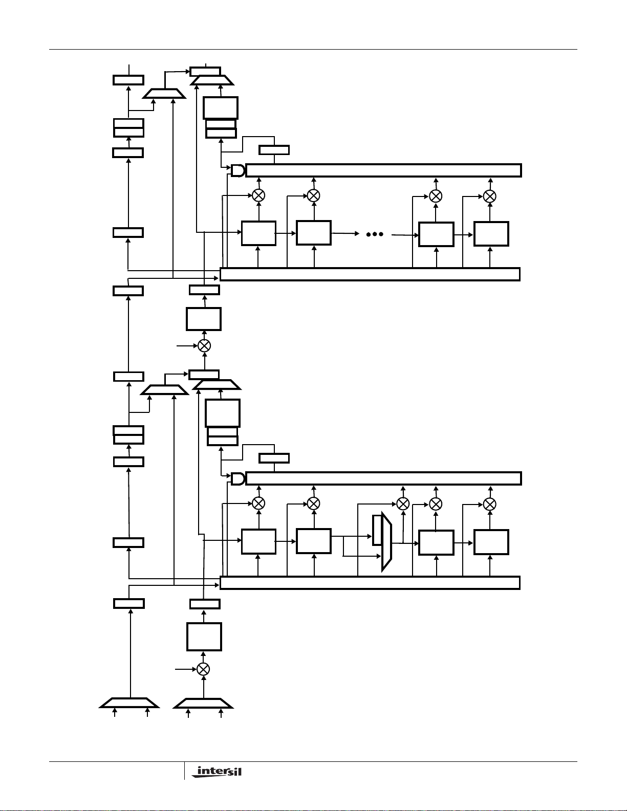
FIR Filter Blocks
There are two programmable FIR filters in each channel.
The main function of the first filter, FIR1, is to reduce the CIC
output sample rate and maximize the efficiency of the
second filter, FIR2. FIR2 provides the final filtering for the
channel of interest. FIR1 can compute up to 32 taps and has
programmable 20-bit coefficients, 20-bit data inputs, and 24bit outputs. FIR2 can compute up to 64 taps and has
programmable 20-bit coefficients, 20-bit input data, and 24bit output data. FIR1 can compute 4 filter taps per clock and
FIR2 can compute 8. All of the available taps can be utilized
if the overall decimation through the CIC and FIRs is 8 or
more. The impulse response of each FIR can be symmetric
or asymmetric. The decimation for the each FIR is
programmable from 1 to 8.
AGC
MULT
EXTERNAL AGC GAIN
MAG
DETECT
FIFO IHBF
HOIF
I
Q
NOTE:
When loading halfband coefficients, the coefficients must be
centered around the fixed center coefficient, e.g. if there are
23 taps, three compute clocks are required, there are 11 on
either side of the center and multiplier 1 computes C0, C2,
C4, multiplier 2 C6, C8, C10, etc.
If there are 19 coefficients, multiplier 2 computes C4, C6, C8
and multiplier 1 computes Z, C0, and C2, i.e. an extra zero
valued coefficient must be added at each end of the
coefficient set to center the coefficients at the fixed
coefficient.
The filters will have unity gain if the sum of all coefficients is
0
equal to 1 for coefficient bit weighting 2
. . . 2
-19
I
Q
To maximize dynamic range, the output bit width of the CIC
and each FIR is 24 bits. A programmable gain stage is
provided before each FIR to compensate for losses in
preceding stages and round to the 20-bit FIR input bit width.
Gains of 1, 2, 4, or 8 can be programmed. Saturation logic is
provided to prevent overflow.
FIR1 includes a half-band filter mode where a fixed center
coefficient of 0.5 is added and the zero valued half-band
coefficients are skipped in the computation. This allows FIR1
to compute a 15-tap half-band filter in two clock cycles or a
31-tap half-band filter in four clock cycles.
14
Page 15
ISL5416
www.BDTIC.com/Intersil
E
R
G
E
R
G
E
R
G
E
R
G
E
R
G
E
R
G
E
R
G
MUX
MUX
LIMIT
DET
RND
E
R
G
E
R
G
E
R
G
4...-30
BYPASS
0...-19
1
REG
FILE
0...-19
R
LIMIT
E
DET
G
RND
REG
0
FILE
A D D
6
REG
FILE
C O N T R O L
REG
7
FILE
x1, 2, 4, 8
E
R
G
E
R
G
E
R
G
E
R
G
E
R
G
E
R
G
MUX
0...-23
E
R
G
MUX
LIMIT
DET
RND
E
R
G
E
R
G
E
R
G
4...-30
0
REG
FILE
0...-19
E
R
G
LIMIT
DET
RND
1
REG
FILE
REG
0 / 0.5
FIXED
MUX
C O N T R O L
A D D
REG
FILE
2
REG
3
FILE
ENABLE
MUX
x1, 2, 4, 8
0...-23
MUX
FIGURE 4. FIR1 AND FIR2 BLOCK DIAGRAMS
15
Page 16

ISL5416
www.BDTIC.com/Intersil
AGC
The automatic gain control (AGC) section adds gain to
maintain the output signal level at a programmed level. The
AGC moderates signal level variation at the output of the
part and reduces the number of bits that must be carried in
any post processing. In the ISL5416, the AGC follows the
channel filtering. The gains through the NCO, mixer, and FIR
filter sections are fixed gains and do not induce AM distortion
before the large interfering signals can be filtered out. If large
interfering signals are not removed by the filtering prior to the
AGC, the gain adjustments by the AGC can AM modulate
the large signals and cause AM sidebands to fall inside the
frequency band of interest.
A block diagram of the A GC is included in figure 6. The AGC
consists of a forward gain path and a loop filter path. In the
forward gain path, the I/Q samples are scaled by the AGC
forward gain value provided by the loop filter. The forward
path gain is divided between a barrel shifter and a multiplier.
The overall forward path gain range is 0 to 96.33 dB. The
barrel shifter provides 0 to 90 dB of gain in steps of 6 dB.
The multiplier provides linear gain between 1.0 and 2.0.
Saturation is provided if there is overflow. The AGC only
adds gain. The loop filter path computes the gain error, filters
it, compares it to gain limits, and provides it to the forward
gain path, to the uP interface, and to the output section. In
the loop filter path the gain error is computed by first
computing the magnitude of the forward path output. The
magnitude is then subtracted from a programmable
threshold or set point. The resulting error value is then
scaled by a programmable loop gain and integrated and
provided to the forward path. Programmable limits on the
forward gain allow the user to restrict the gain to a smaller
range than the 96 dB provided.
The forward gain control word and programmable gain limits
are floating-point numbers consisting of a four-bit exponent
that controls the barrel shifter and a mantissa portion that
controls the multiplier. The barrel shifter gain is 2
multiplier gain is 16 bits, but the two MSBs are fixed at “01”
and are not included in the gain control word. The mantissa
MSB is therefore weighted as 0.5 and the mantissa gain is
1.0 + MANT. The total AGC gain in dB is then:
20*log
The AGC range is then 0 to 96.33 dB for the EXP range of 0
to 15 and MANT range from 0 to 1. Plots of AGC gain versus
the control word are provided in figures 5A and 5B.
The AGC gain word is available through the uP interface and
as a real time output. The gain word is inversely proportional
to the received signal strength in the channel. Signal
strength in dB can be easily estimated by complementing the
gain word and adding an offset equal to the fixed receive
path gain in dB.
10
EXP
( 2
* (1.0 + MANT)).
EXP
. The
The AGC includes a set of counters to synchronize the AGC
to system timing. The counters can be aligned to the
SYNCInX signals if enabled in IWA *000h. One counter is
programmed to count modulo N clocks where N is the length
of the time slot. This counter can be restarted with SYNCInX
to align/re-align it with the slots. A second counter counts out
a delay from the SYNCInX or counter-generated sync. This
delays the AGC timing from the SYNCInX signal to
compensate for filter group dela y or other system delays. A
third counter counts out an interval. The interval can be used
to divide the slot into fast and slow update periods (timed
mode) or into measurement and update periods (sampled
mode). The counters can also be disabled and the AGC
allowed to free run (continuos mode).
A programmable data delay can be inserted in the forward
data path. The loop filter uses the samples into the delay for
computing the new forward gain. The forward gain is then
applied to the samples coming out of the delay. The gain
applied to the output can be continuously updated or can be
updated under the control of the counters. When updated
continuously, the delay causes the forward gain to be based
on samples before and after the delayed sample. This
moderates large signal variations and minimizes the amount
of time that the forward path may be in saturation or be at a
small level.
The sampled mode is used for burst type signals where the
gain adjustment is made during the first part of the burst and
then held for the duration of the burst. The programmable
delay can be set so that the first samples of the burst are
exiting the delay when the gain is updated. In this mode, the
gain may have large instantaneous changes, so proper
timing alignment is very important.
In the timed mode, loop filter continuously updates the
forward gain but uses one set of loop gains during part of the
burst and another set for the rest of the burst. This allows the
time slot to be divided into adapt/hold or fast/slow intervals.
The maximum throughput of the AGC depends on the mode.
In the continuous (counters disabled) and timed modes
without delay, the minimum spacing between samples into
the AGC is 2 clocks. When the delay is enabled, this
increases to 4. In the sampled mode, the delay is always
enabled and the minimum spacing is 4. The minimum
spacing is 1 when the AGC is bypassed.
The AGC loop feedback path includes a magnitude
computation, an error detector, error scaling (loop gain), and
a loop filter. The magnitude computation in the loop filter is a
multi-pass operation with one pass computed per clock
cycle. The accuracy of the computation depends on the
number of passes. The minimum number of clocks between
samples into the AGC is 2. There is a gain in the magnitude
computation that must be taken into account when
programming the AGC set point. This gain also depends on
16
Page 17
ISL5416
www.BDTIC.com/Intersil
the number of passes in the computation. A listing the
accuracy and gain is provided below.
TABLE 5. AGC MAGNITUDE COMPUTATION ACCURACY AND
GAIN
PASSES ERROR +/- (dB) GAIN
2 0.48 1.581
3 0.13 1.630
4 0.03 1.642
8 0.0001 1.647
With maximum gain and with full scale I and Q inputs equal
to ~+/-1.0, the maximum output from the computation is
1.414 * 1.647 = 2.329. The error detector subtracts the
magnitude from the programmable AGC Threshold value.
The AGC Threshold value is set in IWA register *009h and
should be programmed to K times the desired magnitude of
the I/Q where K is the gain of the magnitude computation.
Two adjustment/settling modes are provided in the ISL5416.
In the mean settling mode, the loop adjusts the gain so that
the average magnitude is equal to the programmed set point.
In this mode, the error is scaled by the loop gain and
integrated to compute the forward gain. The loop settles to
the final value asymptotically because the size of the
adjustment decreases as the error decreases. The initial
settling from large errors is fast, but the final pull in is slower .
After the loop has settled, the small adjustment size causes
minimal AM distortion of the signal. The other settling mode
is the median mode. In this mode, the sign of the error is
used increase or decrease the gain by a fixed amount. The
amount of the adjustment is programmed by the loop gain.
The loop settles to the point where there are an equal
number of samples above and below the set point. The loop
settling is roughly linear in dB, but after the loop has settled,
the step size remains the same, so the amount of AM
distortion may be objectionable. The ISL5416 provides two
programmable loop gains, each with a separate attack and
decay settling. The micro-processor can control the loop
gain, or the AGC counters can select the loop gain, so a
large loop gain can be used for initial settling and a smaller
one for tracking. The counters can also select the settling
mode, so the median mode can be used at the beginning of
each time slot and the mean mode used after the initial
settling.
The AGC loop filter is an accumulator (integrator). The
output of the accumulator is the forward gain word that
controls the barrel shifter and multiplier, closing the loop.
There are programmable limits on the accumulator range to
minimize settling time by restricting the AGC to only that
portion of the 96 dB range that is needed. The accumulator
can be loaded by the microprocessor. The gain load is
double buffered-the gain is first loaded into a holding register
by the uP. The gain is then transferred from the holding
register to the accumulator by a write to a special address
location or by the SYNCInX if enabled in IWA *000. The AGC
can be set to a fixed gain either by setting the both upper
and lower gain limits to the desired gain or by setting the
loop gain to zero and programming the accumulator directly.
The bit weighting for the AGC loop is provided in Table 86.
96
84
72
60
48
dB
36
24
12
0
0 32768 65536 98304 131072 163840 196608 229376 262144
FIGURE 5A. ISL5416 AGC FORWARD GAIN RESPONSE
I
6
5
4
3
dB
2
1
0
0 2048 4096 6144 8192 10240 12288 14336 16384
FIGURE 5B. ISL5416 AGC FORW ARD GAIN RESPONSE
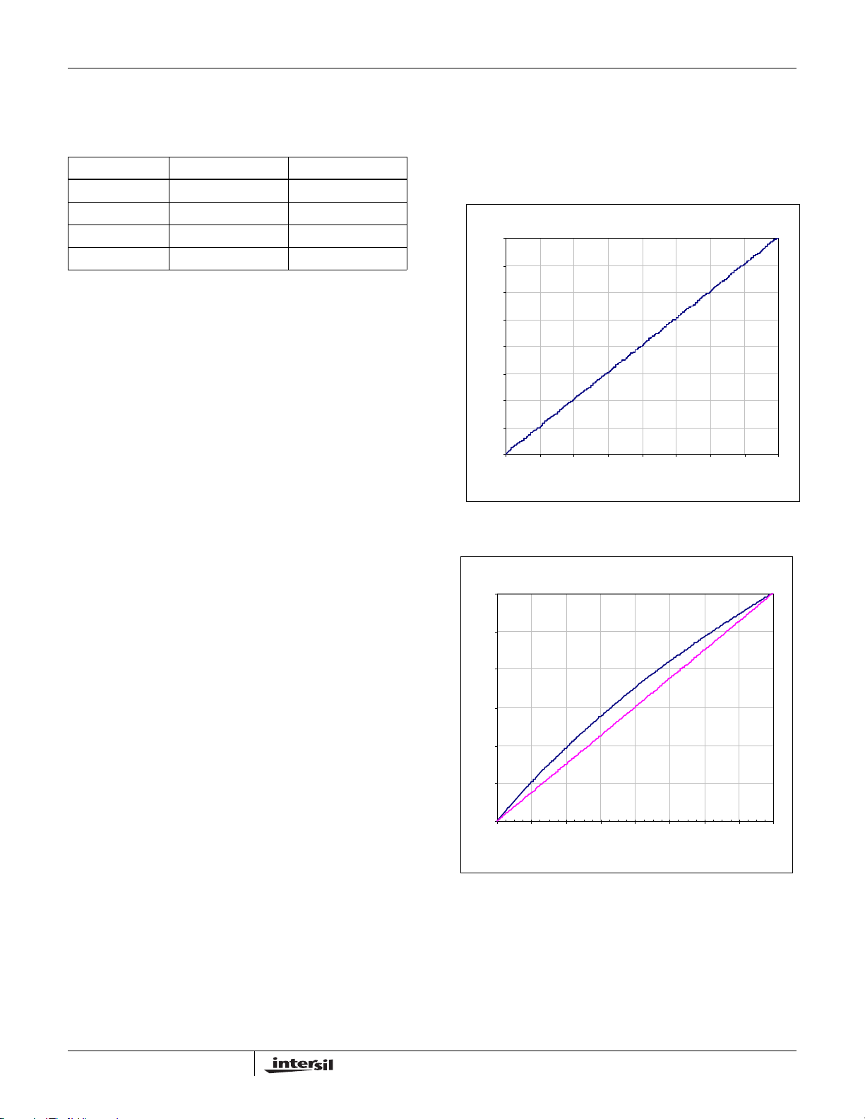
ISL5416 AGC Forward Gain Response
Code
ISL5416 AGC Forward Gain Response
Ma gn i fi ed Vi ew
Code
MAGNIFIED VIEW (ACTUAL AND IDEAL LINEAR
IN dB)
17
Page 18
ISL5416
www.BDTIC.com/Intersil
LIMIT
DETECTOR
E
R
G
MUX
DETECT
OVERFLOW
-5
Z
SAT
CLOCKS
UPPER / LOWER
DECAY 2
DECAY 1
ATTACK 2
ATTACK 1
MEAN/MED 2
MEAN/MED 1
LIMITS
MUX
MUX
SIGN
SIGN
∆
SELECT
LOOP GAIN
SET POINT
Σ
SHIFT
BARREL
MUX
1
2
-4
Z
CLOCKS
| X |
-6
Z
CLOCKS
0
-A
+A
ΥP DATA
DELAY = MAX(1 SAMPLE, 17 CLOCKS)
SAT
MUX
MODE
SAMPLED
GAIN
UPDATE
FORWARD
0
1
E
R
G
SHIFT
BARREL
0 - 63
DELAY
MEMORY
SAMPLES
E
R
G
DETECT
OVERFLOW
SHIFT
BARREL
FIGURE 6. AGC BLOCK DIAGRAM
18
Page 19
ISL5416
www.BDTIC.com/Intersil
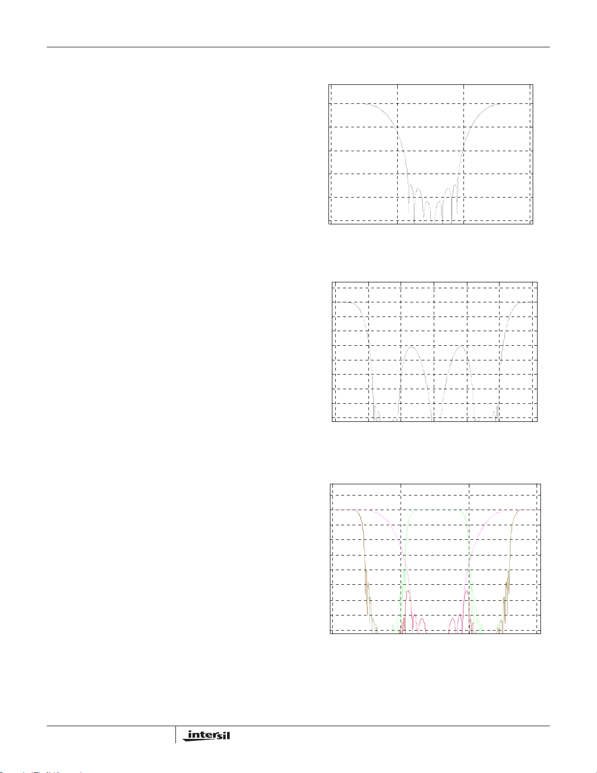
Interpolation Half Band Filter / Re-sampling Filter
A rate change section follows the AGC. This section is used
to resample the signal from FIR2 to increase the sample rate
for finer time resolution and/or to resample the data to
another sample spacing. This section consists of an
interpolation half-band filter, an interpolating resampling
filter, a decimation counter/sampler, a FIFO, a set of NCOs,
and a “leap” counter. This processing stage allows the
filtering in FIR2 to be done at the lowest sample rate that
meets the Nyquist criteria and the data then resampled to
the desired final sample rate. The output/input sample rate
ratio can be almost any value from 0.125 to >4096. A block
diagram is provided below in Figure 8.
The re-sampling filter (HOIF) can accept inputs at any rate
up to its maximum output rate of one half the clock rate.
Preceding the resampler is an interpolation halfband filte r.
This filter can be used to provide a fixed interpolation by 2
when the resampler is bypa sse d or, when used with the
resampler, to increase the image-free dynamic range of the
output. The IHBF can output at up to the clock rate if the
resampling filter is bypassed and up to one half the clock
rate if the resampling filter is enabled. Frequency response
plots are provided below for the half-band and resampling
filters. An example frequency response for a FIR2 response
together with the half-band and resampling filters is also
provided.
The resampling process produces images of the signal at
multiples of the input sample rate. Large interfering signals
must be removed from the spectrum with the CIC, FIR1, and
FIR2 filters or the images created from them in the
resampling process may cause problems. The level of the
images created by resampling process has a fixed dBc level
for a given se t of filters and samplin g ratio . As the signal le v el
in the channel increases and decrease, the images levels
will increase and decrease by the same amount. As the ratio
of the FIR2 output sample rate to the band edge increases,
the level, in dBc, of the images decreases.
0
-2 0
-4 0
-6 0
-8 0
10 0
0 5 10 15
FIGURE 7A. INTERPOLATION HALF BAND RESPONSE
10
0
-1 0
-2 0
-3 0
-4 0
-5 0
-6 0
-7 0
-8 0
0 0.5 1 1.5 2 2. 5 3
FIGURE 7B. IHBF (INTERPOLATE BY 2) AND RE-
SAMPLER (INTERPOLATE BY 2)
10
0
-1 0
-2 0
-3 0
-4 0
-5 0
-6 0
-7 0
-8 0
0 5 10 15
x 10
x 10
x 10
6
7
6
FIGURE 7C. INDIVIDUAL AND COMPOSITE RESPONSES (FIR2
OUTPUT AT 7.68 MHz WITH IHBF, INTERPOLATE BY 2)
19
Page 20
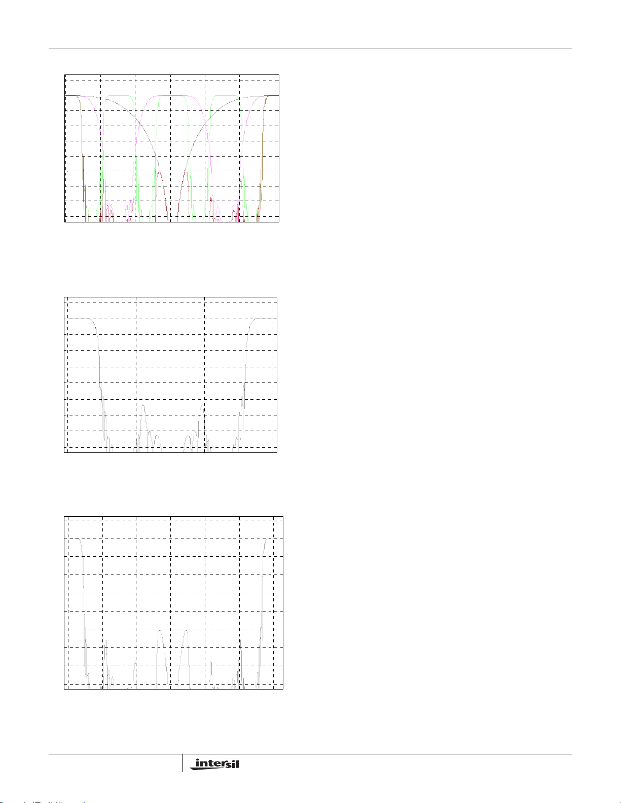
10
www.BDTIC.com/Intersil
0
-1 0
-2 0
-3 0
-4 0
-5 0
-6 0
-7 0
-8 0
0 0. 5 1 1. 5 2 2. 5 3
FIGURE 7D. INDIVIDUAL AND COMPOSITE
RESPONSES (FIR2 OUTPUT AT 7.68 MHz WITH IHBF,
INTERPOLATE BY 2 AND RE-SAMPLER, INTERPOLATE BY 2
x 10
7
ISL5416
Two NCOs and two counters set the sample rates through
the rate change section. NCO1 sets the output sample rate
of the resampling filter. NCO1 is 48 bits and is updated at the
clock rate, so its output frequency is:
Fout
= Fclk * N1 / 248,
1
where N1 is the 48-bit programming word. The carry output
of the phase accumulator is used as the output clock, so
there can be one clock period of jitter. NCO2 is programmed
for the input sample rate to the resampler (equals the halfband filter output rate). NCO2 is updated at the NCO1 output
rate. NCO2 controls the phase of the resampling filter. This
NCO also has a 48-bit phase accumulator. The equation for
programming the output frequency of NCO2 is:
Fout
= Fout1 * N2 / 248 = Fclk * (N1 / 248) * (N2 / 248)
2
when the resampling filter is enabled and
Fout2 = Fclk * N2 / 248
10
0
-1 0
-2 0
-3 0
-4 0
-5 0
-6 0
-7 0
-8 0
0 5 10 15
FIGURE 7E. FIR2 AND IHBF COMPOSITE RESPONSE
10
0
-1 0
-2 0
-3 0
-4 0
-5 0
-6 0
-7 0
-8 0
0 0. 5 1 1.5 2 2.5 3
FIGURE 7F. FIR2, IHBF AND RESAMPLER COMPOSITE
RESPONSE
x 10
x 10
when the resampling filter is bypassed. NCO2 can have one
output sample period (Fout
period) of jitter (one clock
1
period when the HOIF is bypassed).
A static phase offset can be programmed for NCO2. The
range of the phase offset is 0 to 2 NCO2 output sample
periods (0 - 2 resampling filter input sample periods). The
programming resolution is 1/256 of a resampling filter input
sample period. This programmable offset allows the user
vary the group delay of one channel relative to another in
very fine increments to compensate for differ ences in system
delays.
If the resampler is not needed for rate change, it can be used
for phase shifting by setting bit 22 in IWA *001h.
6
While the 48-bit phase accumulators provide very good
frequency programming resolution, at some input/output
sample rate ratios, there will be a slow phase drift due to the
finite word length. To correct for this, a “leap” counter is
provided to reset the phase of the NCOs after a programmed
interval to remove any accumulated error. The leap counter
is 32 bits. If properly programmed, this phase correction will
not be seen in the output of the part.
The input rate to the IHBF/RS section must match the output
sample rate of FIR2, i.e. the output rate of NCO2 must equal
the input sample rate of the part divided by the decimation
factors in the CIC, FIR1, and FIR2. The leap counter can
guarantees this over the long term, but due to the jitter of the
phase accumulator outputs, a FIFO is provided to guarantee
that there are no dropped samples. The FIFO is filled at the
output sample rate of the AGC and is emptied by Fout
Fout
/2 if the IHBF is enabled). After reset, the FIFO is filled
2
2
(or
to a depth of two before the NCOs are enabled. This
7
minimum fill depth guarantees that there are enough
samples in the FIFO that the FIFO never empties or
overflows due to NCO jitter if the NCOs and leap counter are
properly programmed. FIFO reads are enabled after an
20
Page 21
ISL5416
www.BDTIC.com/Intersil
additional 0 to 3 input samples as programmed by the user.
This additional depth provides for additional programmable
group delay. The additional FIFO depth can only be
programmed at reset. Because the NCOs are enabled after
a depth of 2 is reached, the data into the IHBF/Resampler is
zeroed until the programmed fill depth is reached. If both the
half-band and resampling filters are enabled, the
programmable FIFO depth, together with the NCO2 phase
offset, provides from 0 to 4 FIR2 output sample periods of
programmable group delay in 1/512 increments.
Because the IHBF and RS combination can only interpolate,
for resampling ratios <1, the signal must first be interpolated
to a multiple of the desired sample rate and then decimated
LEAP
BY
R
E
G
R
R
E
E
G
G
COUNTER
R
E
G
ROUND
FILL DEPTH BEFORE
ENABLING READS
0, 1, 2, or 3
WR
0...-15
R
E
G
DEPTH =
2 + (0 to 3)
SAMPLES
FIFO
Fihbf_in
RD
IHBF
DIVIDE
1 OR 2
R
E
G
to the final rate. A decimation counter is provided after the
resampling filter to down sample to the desired rate.
The NCO1 and NCO2 frequencies are programmed in IWA =
*011h - *014h. These registers are double buffered. The uP
writes to a holding register. Data is then transf erred to the
active registers by a write to IWA = *017h or b y a SYNCInX if
enabled in IWA = *000h.
The gain data from the AGC is not interpolated. The output
of the AGC is sampled with each I/Q sample to the output
section.
PHASE OFFSET
0 TO 511/256 SAMPLES
Σ
REG
MUX
DIVIDE
R
E
G
Fihbf_out
R
E
MUX
G
Σ
REG
CO
NCO2
FRACTIONAL
R
RESAMPLING
E
INTERPOLATION
G
FILTER
EN
N x Fout
R
R
E
E
G
G
NCO1
R
R
E
E
G
G
Fclk
BY N
Fout
R
E
G
FIGURE 8. IHBF AND RESAMPLER BLOCK DIAGRAM
21
Page 22
ISL5416
www.BDTIC.com/Intersil
Data Output Formatter Section
Four 16-bit output data busses are provided on the ISL5416.
All of the busses share a common output clock, CLKO1,
which is derived from CLKC. CLKO2 signal is provided for
easier board routing or for the differential outputs. Each bus
has an output SYNC which is typically used as a frame sync.
Each bus can be divided into two 8-bit busses if desired.
When a new data sample is available from a channel, it
starts a time slot counter that sequences through up to 8
output time slots. The data type for each time slot is
programmable as well as the FSYNCx assertion. The data
from more than one channel can be multiplexed through the
same output bus if channels are synchronized. The data
from channels 0 and 1 and from channels 2 and 3 can be
multiplexed directly. Multiplexing channels 0 and 1 with 2 and
3 is done by ORing multiplexer outputs together. See figures
10 and 11. This means that related channels (such as
diversity channels) should be grouped into channels 0 and 1,
or into channels 2 and 3 for ease of data routing.
I0 (23:16)
(15:8)
(7:0)
Q0
AGC0
I1
Q1
AGC1 (15:8)
(23:16)
(15:8)
(7:0)
(15:8)
(7:0)
(23:16)
(15:8)
(7:0)
(23:16)
(15:8)
(7:0)
(7:0)
(15:8)
01AC UPPER 16 x 8-BIT MUX
The data type, SYNC assertion, and bus routing are
programmed in registers 0*01h through 0*04h. Two of the
eight time slots are programmed in each location.
The I/Q data from each channel is rounded to 4, 6, 8, 12, 16,
20 or 24 bits at the output of the channel. The AGC gain can
be rounded to 8, 12, or 16 bits. A 24-bit output is provided to
the output section for I and Q data and a 16-bit output is
provided for the AGC data. The data is MSB justified in the
output bus and the LSBs below the programmed number are
zeroed.
24 bits of I/Q data is available from the AGC if the
IHBF/HOIF is bypassed. I/Q are 16 bits if the IHBF/HOIF
section is enabled.
Serial outputs are availa ble . See GW A = 0000h, IW A =
0*06h, 0*07h, and 0*08h.
I0 (23:16)
(15:8)
(7:0)
Q0
AGC0
I1
Q1
AGC1 (15:8)
(23:16)
(15:8)
(7:0)
(15:8)
(7:0)
(23:16)
(15:8)
(7:0)
(23:16)
(15:8)
(7:0)
(7:0)
(7:0)
01AC LOWER 16 x 8-BIT MUX
01 AC UPPER
Channels
Output Byte
Outputs
FIGURE 9. MULTIPLEXING CHANNELS
22
Page 23

MUX #1
www.BDTIC.com/Intersil
CHAN 0 DATA
CHAN 1 DATA
ISL5416
8
64
64
01AC23BD
8
OE_01A
OE_23A
AOUT(15:8)
MUX #3
MUX #2
CHAN 2 DATA
CHAN 3 DATA
CHAN 0 DATA
CHAN 1 DATA
OE_01A
OE_23A
8
64
64
64
64
HIGHLOW
23AC
HIGHLOW
01BD
OE_23C
OE_01C
8
OE_23C
OE_01C
8
OE_01B
OE_23B
8
OE_01B
AOUT(7:0)
COUT(15:8)
COUT(7:0)
BOUT(15:8)
BOUT(7:0)
MUX #4
CHAN 2 DATA
CHAN 3 DATA
23
OE_23B
8
64
64
HIGH HIGHLOWLOW
8
FIGURE 10. OUTPUT ROUTING
OE_23D
OE_01D
OE_23D
OE_01D
DOUT(15:8)
DOUT(7:0)
Page 24

ISL5416
www.BDTIC.com/Intersil
Serial Data Output
The serial data output control register contains sync position
and polarity (SSYNCA, B, C or D), channel multiplexing, and
scaling controls for the SD1x and SD2x (x = A, B, C or D)
serial outputs (see IWA registers 0*06 - 0*08h).
Serial Data Output Time Slot
Content/Format Registers
These two registers are used to program the content and
format of the serial data output sequence time slots (see
IWA registers 0*07h and 0*08h). There are four data time
slots that make up a serial data output stream. The number
of data bits and data format of each slot is programmable as
well as whether there will be a sync generated with the time
slot (the syncs are only associated with the SD1 serial
outputs). Any of three types of data or zeros can be chosen
for each time slot. Seven bits are used to specify the content
and format of each slot.
Channel Routing Mask
The multiplexing mask bits for each channel (see
Microprocessor Interface Section, IWA register 0*06h bits
19:16 for SD1x or bits 15:12 for SD2x) can be used to enable
that channel’s output to any of the four serial outputs. These
bits control AND gates that mask off the channels, so a zero
disables the channel’s connection to that output.
To configure more than one channel's output onto a serial
data output, the SD1 serial outputs and syncs from each
channel (0,1, 2 and 3) are brought to each of the SD1 serial
output sections and the SD2 serial outputs are brought to
each of the SD2 serial output sections (the syncs are only
associated with the SD1 serial outputs). There, the four
outputs are AND-ed with the multiplexing mask programmed
in the serial data output control registers of channels 0 thru 3
and OR-ed together. By gating off the channels that are not
wanted and delaying the data from each desired channel
appropriately, the channels can be multiplexed into a
common serial output stream. It should be noted that in
order to multiplex multiple channels onto a single serial data
stream the channels to be multiplexed must be synchronous.
Microprocessor Interface
The ISL5416 Microprocessor (µP) interface consists of a 16bit bidirectional data bus, P(15:0), three address pins,
ADD(2:0), a write strobe (WR
chip enable (CE
configuration of the ISL5416.
The processor interface to the ISL5416 is a mixture of direct
and indirect addressing. T o minimiz e the amount of
processor address space and bus routing, there are only
eight 16-bit direct address locations. Two of these are used
to access an internal 32-bit bus. To write data to internal
indirect locations, the data is first written to direct addresses
0 (bits 15:0) and 1 (bits 31:16). The internal address is then
). Indirect addressing is used for control and
), a read strobe (RD) and a
written to direct address 2. When the address is written, a
synchronization circuit generates an internal write strobe,
synchronized to the clock, to clock the data into the target
register. The synchronization process requires 4 clock
cycles, so data should not be written to direct addresses 0 or
1 for four cloc k cycles after a write to address 2. To read data
from internal locations, the internal address is first written to
direct address 3. The data can then be read from direct
addresses 0 (15:0) and 1 (31:16). The indirect address
register is shared between direct addresses 2 and 3, with
only writes to address 2 generating write strobes. Because
of this, the address does not have to be re-written to verify a
write unless broadcasting data to more than one channel.
Direct address 2 is used for status when read. The status
bits are defined in Table of Microprocessor Direct
Read/Write Addresses. Direct addresses 4 through 7 are
used for fast read access.
Addresses 4 through 7 (one address per channel) are used
for sequenced read (FIFO-like) addresses. The user can
program the order that the data would be read from the part.
The user can select I, Q, AGC Gain (real time or sampled),
and two types of data from the range control circuit. When a
new output is available , the data type pointer is reset to the
first data type. After each read, the pointer is incremented to
the next data type. To signal a new output on the channel, a
signal can be routed to the CLKO2/INTRPT
enabled to generate interrupt in address IWA = 0*0Ah, bit 31.
If separate interrupt signals are required for each channel,
the FSYNCX pins can be used.
The indirect address space is divided into top level or global
locations for parameters that are shared between channels
or I/Os, I/O control locations, and channel control
parameters. The global locations are between addresses
0000h and 00FFh. The I/O control locations are between
0100h and 0FFFh. Bits 11, 10, 9, and 8 select I/O busses D,
C, B, and A, respectively. What this means is that by setting
a single address bit of 11:8, the control register is written for
that I/O control section. By setting more than one bit, the
same data is written to the corresponding registers of more
than one I/O control section. Reads must select only one I/O
control section.
Channel control registers are located between addresses
1000h and FFFFh. Bits 15, 14, 13, and 12 select channels 3,
2, 1, and 0, respectively. The user can write to individual
channels or to multiple channels at once by setting the
appropriate channel select bit, 15:12. Read addresses must
specify a single channel.
pin. A channel is
24
Page 25

ISL5416
www.BDTIC.com/Intersil
To Write to the Internal Registers:
1. Load the indirect write holding registers at direct address
ADD(2:0) = 0 and 1 with the data for the internal register
(32 bits).
2. Write the Indirect Write Address of the internal register
being addressed to direct address ADD(2:0) = 2 (Note: A
write strobe to transfer the contents of the Indirect Write
Holding Register into the Target Register specified by the
Indirect Address will be generated internally).
3. Wait 4 clock cycles before perf orming the next write to the
indirect write holding registers.
To Read Internal Registers:
1. Write the Indirect Read Address of the internal register
being read to direct address ADD(2:0) = 3.
2. Perform a read of the Indirect Read Holding Registers at
direct address ADD(2:0) = 0 and 1.
NOTE: After an indirect write to a single channel, the data
can be read at direct addresses 0 and 1 after 4 clock
periods.
TABLE 7. STATUS BITS READ DIRECT ADDRESS 2 FOR (15:0)
15:8 REVISION CODE.
0x00h = prototype silicon.
0x01h = production silicon.
JTAG
JTAG: The IEEE 1149.1 Joint Test Action Group boundary
scan standard operational codes shown in Table 2 are
supported. A separate application note is available with
implementation details
JTAG Op Codes Supported
TABLE 6.
INSTRUCTION OP CODE
EXTEST 0000
IDCODE 0001
SAMPLE/PRELOAD 0010
INTEST 0011
BYPASS 1111
7:6 CHANNEL 3 STATUS. Bit 7 is always zero, bit 6 indicates data path saturation.
5:4 CHANNEL 2 STATUS. Bit 5 is always zero, bit 4 indicates data path saturation.
3:2 CHANNEL 1 STATUS. Bit 3 is always zero, bit 2 indicates data path saturation.
1:0 CHANNEL 0 STATUS. Bit 1 is always zero, bit 0 indicates data path saturation.
Bits 0, 2, 4, 6 are the OR-ing together of the individual data
path. Saturation bits listed in *01Fh (Table 14). These bits
are latched when set. Awrite to *01F clears the bit(s).
25
Page 26

ISL5416
www.BDTIC.com/Intersil
TABLE OF MICROPROCESSOR DIRECT READ/WRITE ADDRESSES
ADD(2:0) PINS REGISTER DESCRIPTION
0 WR Indirect Write Data Bus (15:0), “Master (15:0)”.
1 WR Indirect Write Data Bus (31:16), “Master (31:16)”.
2 WR Indirect Write Address Register for Internal Target Register (Generates a write strobe to transfer contents of the
Write Holding Register into the Target Register specified by the Indirect Address, see also Tables of Indirect
Address Registers).
3 WR Indirect Read Address Register (Used to select the Read source of data - uses the same register as Direct
Address 2 but does not generate a write strobe).
4 WR RESERVED
5 WR RESERVED
6 WR RESERVED
7 WR RESERVED
0 RD Indirect Read, Bits 15:0.
1 RD Indirect Read, Bits 31:16.
2 RD Status (15:0).
3 RD RESERVED
4 RD Channel 0 Sequenced Read Address.
5 RD Channel 1 Sequenced Read Address.
6 RD Channel 2 Sequenced Read Address.
7 RD Channel 3 Sequenced Read Address.
Po wer-up Sequencing
The ISL5416 core and I/O blocks are isolated by structures
which may become forward biased if the supply v oltages are
not at specified levels. During the power-up and pow er-down
operations, differences in the starting point and ramp rates of
the two supplies may cause current to flow in the isolation
structures which, when prolonged and excessive, can
reduce the usable life of the device.
In general, the most preferred case would be to power-up
the core and I/O structures simultaneously. However, it is
also safe to power-up the core prior to the I/O block if
simultaneous application of the supplies is not possible. In
this case, the I/O voltage should be applied in 10ms to
100ms nominally to preserve supply component reliability.
Bringing the core and I/O supplies to their respective
regulation levels in a maximum time frame of a 100ms,
moderates the stresses placed on both, the power supply
and the ISL5416.
26
Page 27

ISL5416
www.BDTIC.com/Intersil
Table of Indirect Read and Write Address Registers
NOTE: These Indirect Read Addresses are repeated for each channel. In the addresses below, the * fields are the channel
and I/O select nibble. These bits of the Indirect Address select the target I/O or channel register for the data being read.
TABLE 8. TOP - GLOBAL WRITES
FEDCBA9876543210 DESCRIPTION
0 0 0 0 0 0 0 0 0 0 0 0 0 0 0 0 TOP LEVEL, COMMON OUTPUT CONTROLS AND CHANNEL-TO-CHANNEL
DATA ROUTING
0 0 0 0 0 0 0 0 0 0 0 0 0 0 0 1 RANGE CONTROL TO EOUT MAPPING
0000000000000010uP TEST INPUT DATA, TEST OUTPUT ENABLES
0000000000000011uP TEST DATA STROBE
0000000000000100SYNCO STROBE GENERATION
0000000000000101SYNCO WITH INTERNAL SYNCIn1 FEEDBACK
0 0 0 0 0 0 0 0 0 0 0 0 0 1 1 0 SOFTWARE HARD RESET
0007 - 00FF RESERVED
TABLE 9. TOP - GLOBAL READS
FEDCBA9876543210 DESCRIPTION
0 0 0 0 0 0 0 0 0 0 0 0 0 0 0 0 CONTROL REGISTER 0000h
0 0 0 0 0 0 0 0 0 0 0 0 0 0 0 1 CONTROL REGISTER 0001h
0 0 0 0 0 0 0 0 0 0 0 0 0 0 1 0 CONTROL REGISTER 0002h
0000000000000011N/A (STROBE)
0000000000000100N/A (STROBE)
0000000000000101N/A (STROBE)
0000000000000110N/A (STROBE)
0007 - 00FF RESERVED
TABLE 10. XIN, XOUT, XRNG WRITES (X = A, B, C, D AS SPECIFIED BY * NIBBLE BITS)
FEDCBA9876543210 DESCRIPTION
0000****00000000INPUT FORMAT
0000****00000001PARALLEL OUTPUT ROUTING 1 - TIME SLOTS 0, 1
0000****00000010PARALLEL OUTPUT ROUTING 2 - TIME SLOTS 2, 3
0000****00000011PARALLEL OUTPUT ROUTING 3 - TIME SLOTS 4, 5
0000****00000100PARALLEL OUTPUT ROUTING 4 - TIME SLOTS 6, 7
0000****00000101RANGE CONTROL SYNCInX CONTROLS
0000****00000110SERIAL OUTPUT CONTROL
0000****00000111SERIAL OUTPUT SD1X TIME SLOTS
0000****00001000SERIAL OUTPUT SD2X TIME SLOTS
0000****00001001RANGE CONTROL DC BLOCKING FILTER
0000****00001010SEQUENCED READ ORDER
**** 0*0B - 0*0F RESERVED
0000****00010000RANGE CONTROL CONTROL
27
Page 28

ISL5416
www.BDTIC.com/Intersil
TABLE 10. XIN, XOUT, XRNG WRITES (X = A, B, C, D AS SPECIFIED BY * NIBBLE BITS)
FEDCBA9876543210 DESCRIPTION
00000*0*00010001RANGE CONTROL SLOT PERIOD, DELAY
00000*0*00010010RANGE CONTROL INTEGRATION TIME, NUMBER OF INTEGRATIONS
00000*0*00010011RANGE CONTROL LOWER THRESHOLD, DELTA
00000*0*00010100RANGE CONTROL UPPER THRESHOLD, DELTA
00000*0*00010101RANGE CONTROL IMMEDIATE THRESHOLD, DELTA
00000*0*00010110RANGE CONTROL BIAS
0000****00010111RANGE CONTROL ATTENUATION CONTROL CODES 0 - 3
0000****00011000RANGE CONTROL ATTENUATION CONTROL CODES 4 - 7
0000****00011001RANGE CONTROL uP ATTENUATION ACCUMULATOR LOAD
0000****00011010RANGE CONTROL ACCUMULATOR LOAD STROBE
0000****00011011RANGE CONTROL ACCUMULATOR READ STROBE
0000****00011100RANGE CONTROL INTEGRATOR READ SAMPLE STROBE
0000****00011101RANGE CONTROL DC OFFSET READ SAMPLE STROBE
0*1E - 0*FF RESERVED
x
= These control registers are shared between inputs A and
x
B and between inputs C and D.
x
x
x
x
x
TABLE 11. XIN, XOUT, XRNG READS (X = A, B, C, D AS SPECIFIED BY * NIBBLE BITS)
FEDCBA9876543210 DESCRIPTION
0000*** *00000000CONTROL REGISTER 0*00
0000*** *00000001CONTROL REGISTER 0*01
0000*** *00000010CONTROL REGISTER 0*02
0000*** *00000011CONTROL REGISTER 0*03
0000*** *00000100CONTROL REGISTER 0*04
0000*** *00000101CONTROL REGISTER 0*05
0000*** *00000110CONTROL REGISTER 0*06
0000*** *00000111CONTROL REGISTER 0*07
0000*** *00001000CONTROL REGISTER 0*08
0000*** *00001001CONTROL REGISTER 0*09
0000*** *00001010CONTROL REGISTER 0*0A
0*0B - 0*0F RESERVED
0000*** *00010000CONTROL REGISTER 0*10
0 0 0 0 0 * 0 * 0 0 0 1 0 0 0 1 CONTROL REGISTER 0*11, * = 1, 4 ONLY
0 0 0 0 0 * 0 * 0 0 0 1 0 0 1 0 CONTROL REGISTER 0*12, * = 1, 4 ONLY
0 0 0 0 0 * 0 * 0 0 0 1 0 0 1 1 CONTROL REGISTER 0*13, * = 1, 4 ONLY
0 0 0 0 0 * 0 * 0 0 0 1 0 1 0 0 CONTROL REGISTER 0*14, * = 1, 4 ONLY
0 0 0 0 0 * 0 * 0 0 0 1 0 1 0 1 CONTROL REGISTER 0*15, * = 1, 4 ONLY
0 0 0 0 0 * 0 * 0 0 0 1 0 1 1 0 CONTROL REGISTER 0*16, * = 1, 4 ONLY
0000*** *00010111CONTROL REGISTER 0*17
0000*** *00011000CONTROL REGISTER 0*18
0 0 0 0 * * * * 0 0 0 1 1 0 0 1 RANGE CONTROL LOAD VALUE READ (HOLDING REGISTER)
28
Page 29

ISL5416
www.BDTIC.com/Intersil
TABLE 11. XIN, XOUT, XRNG READS (X = A, B, C, D AS SPECIFIED BY * NIBBLE BITS) (Continued)
FEDCBA9876543210 DESCRIPTION
0000*** *00011010N/A (STROBE)
0 0 0 0 * * * * 0 0 0 1 1 0 1 1 RANGE CONTROL ACCUMULATOR READ AFTER A WRITE TO THIS
0000*** *00011100RANGE SELECT INTEGRATOR READ AFTER A WRITE TO THIS LOCATION
0 0 0 0 * * * * 0 0 0 1 1 1 0 1 RANGE SELECT DC OFFSET READ AFTER A WRITE TO THIS LOCATION TO
TABLE 12. CHANNEL CONTROL REGISTERS (WRITES)
FEDCBA9876543210 DESCRIPTION
** **000000000000CHANNEL SYNC CONTROL
* * * * 0 0 0 0 0 0 0 0 0 0 0 1 CHANNEL DATA PATH, CONTROL
* * * * 0 0 0 0 0 0 0 0 0 0 1 0 CARRIER CENTER FREQUENCY HOLDING REGISTER ♣
* * * * 0 0 0 0 0 0 0 0 0 0 1 1 CARRIER PHASE OFFSET
** **000000000100CARRIER FREQUENCY LOAD STROBE
** **000000000101NCO/CIC CONTROL
* * * * 0 0 0 0 0 0 0 0 0 1 1 0 PN NOISE LEVEL
* * * * 0 0 0 0 0 0 0 0 0 1 1 1 FIR1, FIR2 CINTROL, RE-SAMPLING FILTER OUTPUT DECIMATION
** **000000001000AGC CONTROL
** **000000001001AGC SET POINT
* * * * 0 0 0 0 0 0 0 0 1 0 1 0 AGC UPPER AND LOWER GAIN LIMITS
** **000000001011AGC LOOP GAINS
** **000000001100AGC COUNTER PRELOADS 1
** **000000001101AGC COUNTER PRELOADS 2
** **000000001110AGC uP GAIN LOADING REGISTER
** **000000001111AGC uP GAIN LOADING STROBE
* * * * 0 0 0 0 0 0 0 1 0 0 0 0 AGC STROBE TO SAMPLE GAIN FOR READ
** **000000010001RE-SAMPLING FILTER NCO1 - OUTPUT RATE 47:16
** **000000010010RE-SAMPLING FILTER NCO1 - OUTPUT RATE 15:0 ♣
** **000000010011RE-SAMPLING FILTER NCO2 - INPUT RATE 47:16 ♣
** **000000010100RE-SAMPLING FILTER NCO2 - INPUT RATE 15:0 ♣
* * * * 0 0 0 0 0 0 0 1 0 1 0 1 RE-SAMPLING FILTER NCO2 - PHASE OFFSET/DELAY
** **000000010110RE-SAMPLING FILTER LEAP COUNTER PERIOD
** **000000010111RE-SAMPLING FILTER FREQUENCY UPDATE STROBE
** **000000011000CHANNEL SOFT RESET STROBE
** **000000011001uP STROBE TO UPDATE DATA PATH REGISTER
** ** 00 00 00 01 10 10ADVANCE STROBE
** **000000011011RETARD STROBE
* * * * 0 0 0 0 0 0 0 1 1 1 1 1 CHANNEL STATUS REGISTER CLEAR STROBE
LOCATION TO STABILIZE
TO STABILIZE
STABILIZE
0*1E - 0*FF RESERVED
♣
♣
♣
*01C -*01E RESERVED
29
Page 30

ISL5416
www.BDTIC.com/Intersil
TABLE 12. CHANNEL CONTROL REGISTERS (WRITES) (Continued)
FEDCBA9876543210 DESCRIPTION
*020 -*07F RESERVED
** **000100000000FIR1 COEFFICIENTS
THRU
** **000100011111
*120 - *1FF RESERVED
** **001000000000FIR2 COEFFICIENTS
THRU
** **001000111111
*240 - *FFF RESERVED
The controls marked as “♣” are double buffered, i.e. the data is loaded into a holding register by the uP and then transferred
NOTE:
to an active register by either a write to an indirect location that generates an update strobe or by a SYNCInX signal if enabled in
IWA = *000h.
TABLE 13. CHANNEL CONTROL REGISTERS (READS)
FEDCBA9876543210 DESCRIPTION
** **000000000000CONTROL REGISTER *000
** **000000000001CONTROL REGISTER *001
* * * * 0 0 0 0 0 0 0 0 0 0 1 0 CARRIER ACTIVE CENTER FREQUENCY
** **000000000011CONTROL REGISTER *003
** **000000000100N/A (STROBE)
** **000000000101CONTROL REGISTER *005
** **000000000110CONTROL REGISTER *006
** **000000000111CONTROL REGISTER *007
** **000000001000CONTROL REGISTER *008
** **000000001001CONTROL REGISTER *009
** **000000001010CONTROL REGISTER *00A
** **000000001011CONTROL REGISTER *00B
** **000000001100CONTROL REGISTER *00C
** **000000001101CONTROL REGISTER *00D
* * * * 0 0 0 0 0 0 0 0 1 1 1 0 AGC GAIN IS READ AT DIRECT ADDRESSES 4 - 7 AFTER SAMPLING WITH
A WTITE TO IWA = *010h
** **000000001111N/A (STROBE)
** **000000010000MAGNITUDE (AFTER SAMPLING WITH A WRITE TO THIS LOCATION)
* * * * 0 0 0 0 0 0 0 1 0 0 0 1 ACTIVE RESAMPLER NCO1 FREQUENCY 47:16
* * * * 0 0 0 0 0 0 0 1 0 0 1 0 ACTIVE RESAMPLER NCO1 FREQUENCY 15:0
* * * * 0 0 0 0 0 0 0 1 0 0 1 1 ACTIVE RESAMPLER NCO2 FREQUENCY 47:16
* * * * 0 0 0 0 0 0 0 1 0 1 0 0 ACTIVE RESAMPLER NCO2 FREQUENCY 15:0
** **000000010101CONTROL REGISTER *015
** **000000010110CONTROL REGISTER *016
** **000000010111N/A (STROBE)
** **000000011000N/A (STROBE)
30
Page 31

ISL5416
www.BDTIC.com/Intersil
TABLE 13. CHANNEL CONTROL REGISTERS (READS) (Continued)
FEDCBA9876543210 DESCRIPTION
** **000000011001N/A (STROBE)
* * * * 1 1 0 1 0 N/A (STROBE)
** **000000011011N/A (STROBE)
** **000000011100N/A (STROBE)
*01D - *03E UNUSED
** **000000011111CHANNEL STATUS
*03F - *07F UNUSED
** **0 001 00 000 00 0FIR1 COEFFICIENTS
THRU
** **000100011111
*120 - *1FF UNUSED
** **0 010 00 000 00 0FIR2 COEFFICIENTS
THRU
** **001000111111
*240 - *FFF UNUSED
TABLE 14. CHANNEL STATUS BITS (*01Fh) ONCE SET, STATUS BITS STAY SET UNTIL CLEARED BY A WRITE TO *01Fh
BITS DESCRIPTION
15 FIFO crossed threshold
14 FIFO empty
13 FIFO full
12 Saturation in IHBF (I or Q)
11 Saturation in Q channel 24 -> 16 bit rounder (to FIFO prior to IHBF)
10 Saturation in I channel 24 -> 16 bit rounder (to FIFO prior to IHBF)
9 UNUSED.
8 Saturation in AGC forward gain path (I or Q)
7 Saturation in Q channel FIR2
6 Saturation in I channel FIR2
5 Saturation in Q channel FIR1 to FIR2 gain block
4 Saturation in I channel FIR1 to FIR2 gain block
3 Saturation in Q channel FIR1
2 Saturation in I channel FIR1
1 Saturation in Q channel CIC to FIR1 gain block
0 Saturation in I channel CIC to FIR1 gain block
NOTE: FIR Saturation bits will indicate saturation if an intermediate accumulation exceeds 1.0, even though, the final result is less than 1.0. The
headroom for intermediate sums of products is up to 16 (2
4
).
31
Page 32

ISL5416
www.BDTIC.com/Intersil
Tables of Top Level Registers
In the tables below “reset state” indicates the register
contents after a HW reset or a SW hard reset. Unless
noted, a soft channel reset does not clear register
contents. A soft channel reset does clear the slave
registers of a master/slave pair (such as channel data
path control) but does not clear the master.
TABLE 15. COMMON OUTPUT CONTROL FUNCTIONS (GWA = 0000h) RESET STATE = 0x00000001h
P(31:0) FUNCTION
31 ENABLE SERIAL OUTPUT.
1 = serial output mode is enabled. The DOUT parallel data bus is replaced with 4 serial output busses -- one per channel. See 0*06h
- 0*08h and Table 30.
30 RESERVED. Set to 0.
29 SCLK RESET.
1 = serial clock divider is reset by SYNCInX if the reset serial output bit is set in IWA = *000h, bits 13 or 29 of any of the 4 channels.
28 SCLK POLARITY.
1 = Low to High transitions at the center of the data bit.
0 = High to Low transitions at the center of the data bit.
27:25 SCLK RATE.
000 = SCLK DIsabled.
001 = input clock rate.
010 = input clock rate / 2.
011 = input clock rate / 4.
100 = input clock rate / 8.
101 = input clock rate /16.
This register controls the output SYNC signal polarity, the
output clock rate and polarity, output data modes, and
channel cascading.
24:21 RESERVED. Set to 0.
20 ROUTE CHANNEL 2 TO CHANNEL 3.
19 ROUTE CHANNEL 1 TO CHANNEL 2.
18 ROUTE CHANNEL 0 TO CHANNEL 1.
17 CHANNEL 0 EXTERNAL AGC SOURCE SELECT.
16 CHANNEL 2 EXTERNAL/INTERNAL GAIN CONTROL.
15 CHANNEL 1 EXTERNAL/INTERNAL GAIN CONTROL.
14 CHANNEL 0 EXTERNAL/INTERNAL GAIN CONTROL.
13 CLKO2 OR INTRPT
12 FSYNCX POLARITY.
1 = route the output of FIR2 of channel 2 to the input of the CIC to FIR1 gain block in channel 3.
1 = route the output of FIR2 of channel 1 to the input of the CIC to FIR1 gain block in channel 2.
1 = route the output of FIR2 of channel 0 to the input of the CIC to FIR1 gain block in channel 1.
0 = when bit 14 is set, Channel 1 controls Channel 0 gain.
1 = when bit 14 is set, Channel 3 controls Channel 0 gain.
1 = Channel 2 gain is controlled by Channel 3.
1 = Channel 1 gain is controlled by Channel 3.
1 = Channel 0 gain is controlled by Channel 3 or Channel 1 depending on the state of bit 17.
.
1 = CLKO2/INTRPT
0 = CLKO2/INTRPT
NOTE: For INTRPT
0 = active high
1 = active low.
is INTRPT (2 clock period wide pulse).
is CLKO2.
IWA = 0*0Ah, bit 31 must be set for the channel that is the interrupt source..
32
Page 33

ISL5416
www.BDTIC.com/Intersil
TABLE 15. COMMON OUTPUT CONTROL FUNCTIONS (GWA = 0000h) RESET STATE = 0x00000001h
P(31:0) FUNCTION
11 CLKO2 POLARITY.
1 = Low to High transition in the middle of data period.
0 = High to Low transition in the middle of data period.
If bit 13 is set:
1 = active high interrupt
0 = active low interrupt.
10 CLKO1 POLARITY.
1 = Low to High transition in the middle of data period.
0 = High to Low transition in the middle of data period.
9:8 HOLD CLKO AFTER RESET.
11 = hold CLKO after hard reset until SYNCIn2.
10 = hold CLKO after hard reset until SYNCIn1. (To re-sync the clock after it has been started, disable it by setting these bits to 00
and then set the bits back to 1X and apply SYNCInX).
01 = enable CLKO after programming this register (This applies only when the CLKO rate is NOT equal to CLKIN rate; there is no
need to align the start if CLKO = CLK, and if that is the case, it starts immediately after programming).
00 = disable CLKO.
7:0 CLKO1 RATE.
CLKIN / N for N = 1 to 16.
1 = 0x80h or 0x00h
2 = 0x81h
3 = 0x82h
4 = 0x93h
5 = 0x94h
6 = 0xA5h
7 = 0xA6h
8 = 0xB7h
9 = 0xB8h
10 = 0xC9h
11 = 0xCAh
12 = 0xDBh
13 = 0xDCh
14 = 0xEDh
15 = 0xEEh
16 = 0xFFh
This register (IWA = 0001h) routes the bits from the four
range select blocks to the four nibbles of the Eout bus. Each
nibble of the Eout bus can be controlled by any of the range
selectors. Each range select block contains a mapping table
with three input bits and eight output bits. The three input bits
represent 0 to 42 dB of attenuation in 6 dB steps. The
programming of the input to output bit map depends on the
type of attenuator or VGA used. Ty pically four bits would be
sufficient for an attenuator while 8 bits might be needed for a
D/A controlled VGA.
An example programming for 4 bits per attenuator control is:
0x00001357h
range controls A, B, C, and D control Eout bits 15:12, 11:8,
7:4, 3:0, respectively.
For 8 bits per attenuator control:
0x00000145
range controls A and C control Eout bits 15:8 and 7:0,
respectively.
33
Page 34

ISL5416
www.BDTIC.com/Intersil
TABLE 16. Eout (RANGE CONTROL) SOURCE SELECT (GWA = 0001h) RESET STATE = 0x00000000h
P(31:0) FUNCTION
31:16 UNUSED.
15:12 Eout(15:12).
1XXX = set to 0000.
0000 = AH (A range select mapped bits 7:4).
0001 = AL (A range select mapped bits 3:0).
0010 = BH (B range select mapped bits 7:4).
0011 = BL (B range select mapped bits 3:0).
0100 = CH (C range select mapped bits 7:4).
0101 = CL (C range select mapped bits 3:0).
0110 = DH (D range select mapped bits 7:4).
0111 = DL (D range select mapped bits 3:0).
See IWA = 0*17h and 0*18h.
11:8 Eout(11:8).
See bits 15:12.
7:4 Eout(7:4).
3:0 Eout(3:0).
See bits 15:12.
See bits 15:12.
A test register is provided for the processor to input data to
the part. The register can be selected as the input for any or
all of the channels. The test input is 16 bits of data plus 3 bits
of exponent. The input enable is also controllable by the uP.
clock wide input enable each time the uP writes to IWA =
0003h. This last choice is for inputting test data via the uP
interface. The Input enable choice is done in the channel at
IWA = *001h, bits 19:17.
The choices are always active, always inactive, and one
TABLE 17. TEST INPUT DATA REGISTER (GWA = 0002h) RESET STATE = 0x00000000h
P(31:0) FUNCTION
31:26 RESERVED. Set to 0.
25 RESERVED. Set to 1.
24 RESERVED. Set to 0.
23 ENABLE TESTOUT D(15:0) TO DOUT(15:0). Set to 0 for normal operation. See Table 18 below.
22 ENABLE TESTOUT C(15:0) TO COUT(15:0). Set to 0 for normal operation. See Table 18 below.
21 ENABLE TESTOUT B(15:0) TO BOUT(15:0). Set to 0 for normal operation. See Table 18 below.
20 ENABLE TESTOUT A(15:0) TO AOUT(15:0). Set to 0 for normal operation. See Table 18 below.
19 RESERVED. Set to 0.
18:16 EXPONENT.
000 = add 0 dB of gain.
111 = add 42 dB of gain.
15:0 DATA. Twos complement.
TABLE 18. TESTOUT X(15:0) BUS SIGNALS (CAN BE OR’d WITH NORMAL OUTPUT ON XOUT BY SETTING BITS 23:20, GWA = 0002h)
15 RANGE CONTROL END OF INTEGRATION PERIOD SIGNAL.
14 RANGE CONTROL END OF DELAY SIGNAL
13 RANGE CONTROL COUNTER LOAD SIGNAL (SYNC and slot counter generated)
12 RANGE CONTROL MAGNITUDE GREATER THAN IMMEDIATE THRESHOLD
11 RANGE CONTROL AVERAGE MAGNITUDE GREATER THAN THRESHOLD 2
10 RANGE CONTROL AVERAGE MAGNITUDE SMALLER THAN THRESHOLD 3
9 RESAMPLER NCO2 2X CARRY OUT
34
Page 35

ISL5416
www.BDTIC.com/Intersil
TABLE 18. TESTOUT X(15:0) BUS SIGNALS (CAN BE OR’d WITH NORMAL OUTPUT ON XOUT BY SETTING BITS 23:20, GWA = 0002h)
8 RESAMPLER NCO1 2X CARRY OUT
7 AGC COUNTER LOAD SIGNAL (SYNC and slot counter generated)
6 AGC END OF DELAY COUNTER
5 AGC LOOP GAIN SELECT SIGNAL
4 AGC UPDATE FORWARD GAIN SIGNAL
3 CARRIER NCO MSB (L.O. TEST POINT)
2:0 FIFO READ ADDRESS (2:0); (FIFO Depth, empty = 0)
TABLE 19. TEST INPUT STROBE (GWA = 0003h) RESET STATE = INACTIVE
N/A FUNCTION
N/A STROBE. A write to this location generates a one-clock-wide test input enable (for use with the test input register).
For synchronization of the ISL5416 channels to system
timing and/or to the processing of other ISL5416 channels,
one synchronization output (SYNCO) and two
synchronization inputs (SYNCIn1 and SYNCIn2) are
provided. The SYNCO of one ISL5416 might be connected
to the SYNCIn1 of all the ISL5416s to allow the uP to
synchronously start or update parameters in all of the
ISL5416s. A write to IWA = 0005h also internally routes the
SYNCO to the SYNCIn1 input with the same delay as
TABLE 20. SYNCO (GWA = 0004h) RESET STATE = INACTIVE
N/A FUNCTION
N/A STROBE. A write to this location generates a one-clock-wide pulse on the SYNCO pin.
TABLE 21. SYNCO WITH INTERNAL FEEDBACK (GWA = 0005h) RESET STATE = INACTIVE
N/A FUNCTION
N/A STROBE. A write to this location generates a one-clock-wide pulse on the SYNCO pin that is also internally fed back to the
SYNCIn1 pin.
There are three resets to the ISL5416 -- the reset pin, the
chip hard reset (IWA = 0006h), and the soft channel reset
(IWA = *018h). The pin reset and chip hard reset have the
same effect. The soft channel reset only affects the selected
connecting the SYNCO pin to the SYNCIn1 pin. For
alignment to system timing, the SYNCInX pins can be
connected to any one-clock-wide signal synchronous to
CLKC. A second synchronization input, SYNCIn2, is
provided to synchronize different channels to different event
or to allow the processor to control certain events and the
system timing to control others.
channel and does not reset the control registers, only the
slave (active) registers of master/slave pairs.
TABLE 22. CHIP HARD RESET VIA SOFTWARE (GWA = 0006h) RESET STATE = INACTIVE
N/A FUNCTION
N/A RESET STROBE. Writing to this location generates a hardware reset, resetting all control registers. Identical function to the RESET
pin.
35
Page 36

ISL5416
www.BDTIC.com/Intersil
Tables of I/O Registers
TABLE 23. CHANNEL INPUT FORMAT (IWA = 0*00h) RESET STATE = 0x00000000h
P(31:0) FUNCTION
31:16 UNUSED.
15 FIXED GAIN MODE IN VGA.
14 RESERVED. Set to 1.
13 INVERT INPUT CLOCK.
1 = High -> Low edge of the input clock samples input data.
0 = Low -> High edge of the input clock samples input data.
12 INPUT CLOCK SOURCE.
1 = CLKC
0 = CLKA for Ain (address 0000 XXX1 0000 0000)
CLKB for Bin (address 0000 XX1X 0000 0000)
CLKD for Din (address 0000 1XXX 0000 0000)
CLKC is always used for Cin
The rising edge of CLKC is always used for the channel processing and output timing.
11 INPUT FORMAT.
10 GATED & INTERPOLATED.
9:7 DEMUX DELAY.
6:5 RESERVED. Set to 0.
3:2 FIXED/FLOATING POINT MODE.
1:0 RESERVED. Set to 0.
1 = offset binary.
0 = 2’s complement
1 = input interpolated.
0 = input gated.
000 = no delay, take sample aligned with the enable.
111 = take 7th sample after the enable.
4 LSB TO MSB SWAP ON DATA.
1 = input bus reversed MSB for LSB -- XIN(0) = MSB.
0 = input bus normal XIN(16) = MSB
Provided to simplify circuit board routing.
00 = 16-bit fixed point (bits 16:1, 0 unused).
01 = 14/3 floating point (bits 16:3 mantissa, 2:0 exponent).
10 = 15/2 floating point (bits 16:2 mantissa, 1:0 exponent).
11 = 16/1 floating point (bits 16:1 mantissa, 0 exponent).
36
Page 37

ISL5416
www.BDTIC.com/Intersil
TABLE 24. XOUT DATA VERSUS TIME SLOT ROUTING, TIME SLOTS 0, 1 (IWA = 0*01h) RESET ST ATE = 0x00000000h
X = A, B, C, D (Descriptions below are for the channels 0/1 multiplexer IWA = 0101h (MUX 01A C). See figure 10 for corresponding signals
P(31:0) FUNCTION
31:30 RESERVED. Set to 0.
29:28 XOUT TIMING SOURCE. The output slot counter is started by a new sample from
00 = Channel 0
01 = Channel 1
10 = Channel 2
11 = Channel 3
This allows two output busses to be used by one channel if the other channel is disabled.
27 INVERT (ONES COMPLEMENT) XOUT BUS.
1 = ones complement XOUT(15:0). By setting this bit for BOUT or DOUT, the AOUT and BOUT and/or COUT and DOUT can provide
complementary output signals.
26 ASSERT FSYNCX DURING SLOT 1.
1 = assert FSYNCX for this time slot.
0 = no FSYNCX.
25 ENABLE TO Cout DURING SLOT 1. (OE_01C)
1 = route the data selected in 23:16 and SYNC enabled in bit 26 to the Cout and SYNCC pins. Provided for multiplexing A and B with
C and D channels.
24 ENABLE TO Aout DURING SLOT 1. (OE_01A)
1 = route the data selected in 23:16 and SYNC enabled in bit 26 to the Aout and SYNCA pins. Provided for multiplexing A and B with
C and D channels.
23:20 SLOT 1, HIGH BYTE. Data output from the A high byte multiplexer for slot 1. See Table 29 for coding.
19:16 SLOT 1, LOW BYTE. Data output from the A low byte multiplexer for slot 1. See Table 29 for coding.
15:11 RESERVED. Set to 0.
10 ASSERT FSYNCX DURING SLOT 0.
1 = assert FSYNCX for this time slot.
0 = no FSYNCX.
9 ENABLE TO Cout DURING SLOT 0.
1 = route the data selected in 7:0 and SYNC enabled in bit 10 to the Cout and SYNCC pins. Provided for multiplexing A and B with
C and D channels.
8 ENABLE TO Aout DURING SLOT 0.
1 = route the data selected in 7:0 and SYNC enabled in bit 10 to the Aout and SYNCA pins. Provided for multiplexing A and B with
C and D channels.
7:4 SLOT 0, HIGH BYTE. Data output from the A high byte multiplexer for slot 0. See Table 29 for coding.
3:0 SLOT 0, LOW BYTE. Data output from the A low byte multiplexer for slot 0. See Table 29 for coding.
and buses for the other multiplexers)
TABLE 25. XOUT DATA VERSUS TIME SLOT ROUTING, TIME SLOTS 2, 3 (IWA = 0*02h) RESET STATE = 0x00000000h
P(31:0) FUNCTION
31:27 RESERVED. Set to 0.
26:16 SLOT 3 CONTROL (see Table 24)
15:11 RESERVED. Set to 0.
10:0 SLOT 2 CONTROL (see Table 24)
TABLE 26. XOUT DATA VERSUS TIME SLOT ROUTING, TIME SLOTS 4, 5 (IWA = 0*03h) RESET STATE = 0x00000000h
P(31:0) FUNCTION
31:27 RESERVED. Set to 0.
26:16 SLOT 5 CONTROL (see Table 24)
15:11 RESERVED. Set to 0.
10:0 SLOT 4 CONTROL (see Table 24)
37
Page 38

ISL5416
www.BDTIC.com/Intersil
TABLE 27. XOUT DATA VERSUS TIME SLOT ROUTING, TIME SLOTS 6, 7 (IWA = 0*04h) RESET STATE = 0x00000000h
P(31:0) FUNCTION
31:27 RESERVED.
26:16 SLOT 7 CONTROL (see Table 24)
15:11 RESERVED.
10:0 SLOT 6 CONTROL (see Table 24)
The ISL5416 can be programmed to respond to the
synchronization inputs, SYNCIn1 and SYNCIn2, in a number
of ways. This register controls the range control response to
TABLE 28. INPUT SYNCIn1/SYNCIn2 FUNCTION SELECT (IWA = 0*05h) RESET STATE = 0x00000000h
P(31:0) FUNCTION
31 ENABLE SYNCIn2 TO RANGE CONTROL.
1 = range control block responds to SYNCIn2 according to bits 19:16 settings.
0 = range control block does not respond to SYNCIn2.
30:20 RESERVED. Set to 0.
19 READ UPDATE ON SYNCIn2.
1 = attenuator control accumulator contents are transferred to the read holding register on SYNCIn2.
18 LOAD ACCUMULATOR ON SYNCIn2.
1 = attenuator control accumulator is loaded from the uP load register (0*19) on a SYNCIn2.
17 RANGE CONTROL STARTUP ON SYNCIn2.
1 = enable range control on SYNCIn2 if 0*10, bit 1 is set. Range control is disabled on reset or by writing a zero to IWA = 0*10h, bit
0. If this bit is set, bit 0 of 0*10 is set on a SYNCIn2.
16 TIMING RESET ON SYNCIn2.
1 = reset range control timing on SYNCIn2 if 0*10, bit 1 is set. Once started, the timers will run until disabled (bit 1 of 0*10h or HW
reset).
15 ENABLE SYNCIn1 TO RANGE CONTROL.
1 = range control block responds to SYNCIn1 according to bits 3:0 settings.
0 = range control block does not respond to SYNCIn1.
the SYNC inputs. The response of the channels to the SYNC
inputs is controlled by IWA = *000h. CLKO start up from
SYNCIn1 or SYNCIn2 is controlled in IWA = 0000h.
14:4 RESERVED. Set to 0.
3 READ UPDATE ON SYNCIn1.
1 = attenuator control accumulator contents are transferred to the read holding register on SYNCIn1.
2 LOAD ACCUMULATOR ON SYNCIn1.
1 = attenuator control accumulator is loaded from the uP load register (0*19) on a SYNCIn1.
1 RANGE CONTROL STARTUP ON SYNCIn1.
1 = enable VGA startup control on SYNCIn2 if 0*10, bit 1 is set. Range control is disabled on reset or by writing a zero to 0*10, bit 0.
If this bit is set, bit 0 of 0*10 is set on a SYNCIn1. Disable on reset.
0 TIMING RESET ON SYNCIn1.
1 = reset range control timing on SYNCIn1 if 0*10, bit 1 is set. Once started, the timers will run until disabled (bit 1 of 0*10h or HW
reset).
38
Page 39

ISL5416
www.BDTIC.com/Intersil
T ABLE 29. HIGH, LOW BYTE DAT A TYPE CODES (AFTER
ROUNDING IN THE CHANNEL)
CHANNEL 0, CHANNEL
CODE
0000 CH 0 I(23:16) CH 2 I(23:16)
0001 CH 0 I(15:8) CH 2 I(15:8)
0010 CH 0 I(7:0) CH 2 I(7:0)
0011 CH 0 Q(23:16) CH 2 Q(23:16)
0100 CH 0 Q(15:8) CH 2 Q(15:8)
0101 CH 0 Q(7:0) CH 2 Q(7:0)
0110 CH 0 AGC(15:8) CH 2 AGC(15:8)
0111 CH 0 AGC(7:0) CH 2 AGC(7:0)
1000 CH 1 I(23:16) CH 3 I(23:16)
1001 CH 1 I(15:8) CH 3 I(15:8)
1010 CH 1 I(7:0) CH 3 I(7:0)
1011 CH 1 Q(23:16) CH 3 Q(23:16)
1100 CH 1 Q(15:8) CH 3 Q(15:8)
1 MUXES
CHANNEL 2, CHANNEL
3 MUXES
Serial Output:
When bit 31 of GWA = 0000h is set, the DOUT bus is used
for serial outputs.
Four bits are allocated to each channel as follows:
TABLE 30. SERIAL OUTPUT BITS ALLOCATION
CHANNEL 0 CHANNEL 1 CHANNE L 2 CHANNEL 3
SCLKX DOUT0 DOUT4 DOUT8 DOUT12
SSYNCX DOUT1 DOUT5 DOUT9 DOUT13
SD1X DOUT2 DOUT6 DOUT10 DOUT14
SD2X DOUT3 DOUT7 DOUT11 DOUT15
A common serial clock generator is used for all four outputs,
so the four SCLKs are synchronous. Four separate outputs
are provided to simplify PWB routing. Each SCLK output can
be separately enabled, so th at unused clock outputs can be
turned off.
Serial outputs are always MSB first.
Addresses 0106h to 0108h control the serial output from
channel 0.
1101 CH 1 Q(7:0) CH 3 Q(7:0)
1110 CH 1 AGC(15:8) CH 3 AGC(15:8)
1111 CH 1 AGC(7:0) CH 3 AGC(7:0)
Addresses 0206h to 0208h control the serial output from
channel 1.
Addresses 0406h to 0408h control the serial output from
channel 2.
Addresses 0806h to 0808h control the serial output from
channel 3.
39
Page 40

ISL5416
www.BDTIC.com/Intersil
TABLE 31. SERIAL OUTPUT CONTROL (IWA = 0*06h) RESET STATE = 0x00000000h
P(31:0) FUNCTION
31:30 RESERVED. Set to 0.
29 SCLK ENABLE.
1 = enable
The serial clock generator is shared by the four serial outputs. A serial clock pin is provided for each output. Each pin can be enabled
or disabled independent of the other channels.
28 SSYNCX POLARITY.
27:26 RESERVED. Set to 0.
25:24 SSYNCX POSITION.
23:20 RESERVED. Set to 0.
19:16 SD1X ROUTING MASK.
15:12 SD2X ROUTING MASK.
1 = Active Low.
0 = Active High.
The SSYNCX signal is asserted for one serial clock period for each time slot where SSYNC is enabled.
00 = Early SSYNC. SSYNCX is asserted during the serial clock period prior to the first data bit for each slot where SSYNC is enabled.
01 = Late SSYNC. SSYNCX is asserted during the serial clock period following the last data bit for each slot where SSYNC is enabled.
1X = Coincident SSYNC. SSYNCX is asserted during the serial clock period of first data bit for each slot where SSYNC is enabled.
These bits gate the serial output of each channel to any or all 4 serial output pins. The gated serial outputs from all of the channels
are ORed together. This allows channels to be multiplexed together on a single serial output by offsetting the serial data streams from
each other using the hold off delay below or by using empty time slots. Note that the serial data from each channel is zeroed after all
of the slots have been output, so it will not interfere with a delayed channel. The multiplexing of the SSYNCX signals matches the
data multiplexing.
19 - Enable the serial output to the SD1D pin.
18 - Enable the serial output to the SD1C pin.
17 - Enable the serial output to the SD1B pin.
16 - Enable the serial output to the SD1A pin.
15 - Enable the serial output to the SD2D pin.
14 - Enable the serial output to the SD2C pin.
13 - Enable the serial output to the SD2B pin.
12 - Enable the serial output to the SD2A pin.
11:0 OUTPUT HOLD OFF DELAY.
P(31:0) FUNCTION
31 SLOT 4 SYNC ENABLE.
30:27 SLOT 4 WORD WIDTH.
These bits control a programmable hold off delay from the time a set of data samples is provided to the serial output section to the
time that the serial output begins. The delay is programmed in serial clocks. Program with the desired number of serial clocks:
0 = no delay
TABLE 32. SERIAL OUTPUT SD1X SLOT CONTROL (IWA = 0*07h) RESET STATE = 0x00000000h
1 = SSYNCX active for this time slot
0 = no SSYNCX for this time slot
0000 = 0-bit*
0001 = 4-bit
0010 = 6-bit
0011 = 8-bit
0100 = 10-bit
0101 = 12-bit
0110 = 16-bit
0111 = 20-bit
1000 = 24-bit
1001 = 32-bit (8 LSBs zeroed)
All other codes are invalid. Note that if the channel output is rounded to fewer than 24 bits and fewer than 24 bits is selected for the
slot width, the output will be doubly rounded.
* if 0-bit is selected for slot 1, 2, or 3, one SCLK period will actually be used, though no data will be output.
40
Page 41

ISL5416
www.BDTIC.com/Intersil
TABLE 32. SERIAL OUTPUT SD1X SLOT CONTROL (IWA = 0*07h) RESET STATE = 0x00000000h
P(31:0) FUNCTION
26:24 SLOT 4 DATA TYPE.
23:16 SLOT 3. See bits 31:24.
15:8 SLOT 2. See bits 31:24.
7:0 SLOT 1. See bits 31:24.
P(31:0) FUNCTION
31 RESERVED, Set to 0.
30:27 SLOT 4 WORD WIDTH.
000 = zeros.
001 = I
010 = Q
011 = AGC (real time).
TABLE 33. SERIAL OUTPUT SD2X SLOT CONTROL (IWA = 0*08h) RESET STATE = 0x00000000h
0000 = 0-bit*
0001 = 4-bit
0010 = 6-bit
0011 = 8-bit
0100 = 10-bit
0101 = 12-bit
0110 = 16-bit
0111 = 20-bit
1000 = 24-bit
1001 = 32-bit (8 LSBs zeroed)
All other codes are invalid. Note that if the channel output is rounded to fewer than 24 bits and fewer than 24 bits is selected for the
slot width, the output will be doubly rounded.
* if 0-bit is selected for slot 1, 2, or 3, one SCLK period will actually be used, though no data will be output.
26:24 SLOT 4 DATA TYPE.
23:16 SLOT 3. See bits 31:24.
15:8 SLOT 2. See bits 31:24.
7:0 SLOT 1. See bits 31:24.
P(31:0) FUNCTION
31:19 RESERVED. Set to 0.
18 DC FILTER DISABLE.
17:16 DC FILTER GAIN.
15:0 µP LOADED DC OFFSET. Twos Complement. These bits are subtracted from the 16 mantissa bits. Bit 15 has the same weighting
000 = zeros.
001 = I
010 = Q
011 = AGC (sampled real time, not sampled by µP write or real time updated every AGC input).
TABLE 34. RANGE CONTROL DC BLOCKING FILTER CONTROL (IWA = 0*09h) RESET STATE = 0x00000000h
1 = Clear filter based DC offset, shut off filter
00 = Widest
01 = Medium
10 = Narrowest (roughly 120 Hz HPF at 61.44 MSPS)
11 = use µP programmed DC offset value
as XIN16 (MSB).
41
Page 42

ISL5416
www.BDTIC.com/Intersil
A/D Range Control Registers
The range control section monitors the output of the A/D and
adjusts the RF/IF gain to maintain a desired A/D output
range. The gain adjustments are in 6 dB steps. The levels,
adjustment rates, and gain to bit mapping are
programmable.
A code is programmed for output on the EOUT bus for each
of the eight states of the three MSBs of the attenuator control
register. These codes can be up to 8 bits, but if four gain
control sections are used, only four bits are available for
each gain control section. The routing of the gain control bits
to EOUT bits is done in IWA = 0001h.
TABLE 35. µP SEQUENCED READ MODE, READ ORDER SELECT (IWA = 0*0Ah) RESET STATE = 0x00000000h
P(31:0) FUNCTION
31 1 = Generate an interrupt with each new data output for this channel.
30:28 READ EIGHT. See bits 3:0. Mask off the MSB of the code.
27:24 READ SEVEN. See bits 3:0.
23:20 READ SIX. See bits 3:0.
The range control registers will be explained later in:
IWA = 0*09h - 0*16h and IWA = 0*19h - 0*1Dh
Direct addresses 4-7 have a sequenced read mode for
quickly reading I/Q output data, real time AGC gain, sampled
AGC gain, or range control data. The read order is
programmed in this register. The arrival of a new channel
output sample resets the read pointer to the first data type.
The rising edge of the RD
signal (or DSTRB with RD/WR
high in uP mode 1) will advance the pointer for that channel
to the next data to get it set up at the interface for fast
access. The CLKO2 signal can be programmed as an
interrupt signal for this mode (see GWA = 0000h, bit 13) to
tell the processor when there is a new data. Alternatively, the
frame strobe signals from the channels can be used.
19:16 READ FIVE. See bits 3:0
15:12 READ FOUR. See bits 3:0
11:8 READ THREE. See bits 3:0
7:4 READ TWO. See bits 3:0
3:0 READ ONE. (FIRST READ).
P(31:0) FUNCTION
31:24 IMMEDIATE HOLD OFF.
23:16 UPDATE EXPONENT DELAY.
15 DISABLE ACCUMULATOR UPDATES.
0000 = AGC Gain -- sampled by a write to IWA = *010h
0001 = AGC Gain -- real time (updated with every I/Q)
0010 = Q(7:0), 8 zeros
0011 = Q(24:8)
0100 = I(7:0), 8 zeros
0101= I(24:8)
0110 = range control I&D (see IWA = 0*1Ch)
0111 = range accumulator (see IWA = 0*1Bh)
Note that the I/Q data will be rounded to the number of bits programmed in IWA = *001h bits 5:3, and the real time AGC data will have
the format selected in IWA = *001h, bits 2:0.
TABLE 36. ADC RANGE CONTROL -- MAIN (IWA = 0*10h) RESET STATE = 0x00000000h
Delay in clock cycles after the immediate threshold adjustment before another adjustment is allowed (00000000 = 1 clock delay). Load
with the desired value minus one.
Delay in clock cycles from a change in the VGA value before it is added to the input exponent value. This should be set to equal the
RF/ADC plus the ISL5416 pipeline delays (6 clocks).
1 = disable range control accumulator updates. uP can still load.
42
Page 43

ISL5416
www.BDTIC.com/Intersil
TABLE 36. ADC RANGE CONTROL -- MAIN (IWA = 0*10h) RESET STATE = 0x00000000h (Continued)
P(31:0) FUNCTION
14 TIME USING CLOCKS/SAMPLES.
Count intervals and delays using clocks or input enables.
1 = clocks.
0 = input enables.
13:11 UPPER LIMIT.
10:8 LOWER LIMIT.
7:4 NORMALIZATION SHIFT/DIVIDE SELECT.
NOTE: The range control can be enabled by writing to bit 0 or bit 0 can be set by SYNCInX to start updates. See IWA = 0*05h. Timing reset
Upper attenuator control limit, 0 to 42 dB in 6 dB steps.
000 = 0 dB.
111 = 42 dB.
Lower attenuator control limit, 0 to 42 dB in 6 dB steps.
000 = 0 dB.
111 = 42 dB.
N
Normalizing shifter control. Divides the integrated magnitude by 2
accumulator input bits: 2
accumulator output bits: 216 . . . 2
0000 = select 21 to 2
1111 = select 216 . . .to 2
3 ENABLE INPUT EXPONENT BITS.
Enable the exponent bits from the input to be added to the attenuation control bits and routed to the channel(s).
2 ENABLE RANGE CONTROL EXPONENT BITS.
Enable the attenuator control register (accumulator MSBs) bits to be added to the exponent bits from the input and routed to the
channel(s).
1 ENABLE RANGE CONTROL.
1 = enable the range control.
0 = disable the range control (including timers).
0 ENABLE RANGE CONTROL BITS
Enable changes in the attenuator control register (if this bit is cleared, the timers still run but changes to the register are inhibited.
by SYNCInX is enabled by bits 0 and 16 of IWA = 0*05h.
-14
1
0
. . . 2
-15
-15
prior to threshold comparison:
T ABLE 37. TIME SLOT PERIOD, DELAY FROM SYNCInX TO START OF INTEGRATION (IW A = 0*11h) RESET STATE = 0x00000000h THIS
CONTROL IS SHARED FOR AIN/BIN AND FOR CIN/DIN
P(31:0) FUNCTION
31:16 SYNC DELAY.
Delay from SYNC (external or counter generated) to the start of integration. Range of delay is 1 to 65536, load with the desired value
minus 1. Delay in input samples or clocks as selected by bit 14, IWA = 0*10h.
15:0 SLOT PERIOD.
Time interval between counter generated SYNCs in samples or clocks as selected by bit 14, IWA = 0*10h. Range for period is 2 to
65536, load with period minus 1.
TABLE 38. NUMBER OF INTEGRATIONS PER SLOT, INTEGRATION TIME (IWA = 0*12h) RESET STATE = 0x00000000h
THIS CONTROL IS SHARED FOR AIN/BIN AND FOR CIN/DIN
P(31:0) FUNCTION
31:16 NUMBER OF INTEGRATIONS PER SLOT.
Number of input magnitude integration periods per slot. Range is 1 to 32768, load with number of integrations minus 1.
15:0 INTEGRATION TIME.
Number of input samples to average before making an upper or lower threshold decision in samples or clocks as selected by bit 14,
IWA = 0*10h. Range is 2 to 65536, load with samples minus 1.
43
Page 44

ISL5416
www.BDTIC.com/Intersil
T ABLE 39. LOWER THRESHOLD , ATTENUATOR CHANGE (IWA = 0*13h) RESET STA TE = 0x00000000h THIS
CONTROL IS SHARED FOR AIN/BIN AND FOR CIN/DIN
P(31:0) FUNCTION
31:30 RESERVED. Set to 0.
29:16 ATTENUATION STEP 3.
15:0 THRESHOLD 3.
T ABLE 40. UPPER THRESHOLD, ATTENUATOR CHANGE (IWA = 0*14h) RESET STATE = 0x00000000h THIS
P(31:0) FUNCTION
31:30 RESERVED. Set to 0.
29:16 ATTENUATION STEP 2.
15:0 THRESHOLD 2.
Amount to decrease the attenuation control register if the average input magnitude is below the lower threshold. 14-bit value loads
the LSBs of a 17-bit accumulator. The 3 MSBs of the 17-bit load are hard-wired to “111” , so the load value should be masked from
a negative number. The MSB of the 14-bit value is weighted at 6 dB so the value at all zeros would be ~12 dB (decrease in
attenuation).
Lower threshold value. If the accumulated and normalized input magnitude is below this value, the attenuation control accumulator is
adjusted by the amount programmed in bits 29:16.
CONTROL IS SHARED FOR AIN/BIN AND FOR CIN/DIN
Amount to increase the attenuation control register if the average input magnitude is above the upper threshold. 14-bit value loads
the LSBs of a 17-bit accumulator. The 3 MSBs of the 17-bit load are hard-wired to “000” . The MSB of the 14-bit value is weighted at
6 dB so the value at all ones would be ~12 dB (increase in attenuation).
Upper threshold value. If the accumulated and normalized input magnitude is above this value, the attenuation control accumulator
is adjusted by the amount programmed in bits 29:16.
T ABLE 41. IMMEDIA T E THRESHOLD , ATTENUA TOR GAIN (IWA = 0*15h) RESET ST ATE = 0x00000000h THIS
CONTROL IS SHARED FOR AIN/BIN AND FOR CIN/DIN
P(31:0) FUNCTION
31:30 RESERVED. Set to 0.
29:16 ATTENUATION STEP 1.
15:0 THRESHOLD 1.
Amount to increase the attenuation control register if the sample-by-sample input magnitude is above the immediate threshold. 14bit value loads the LSBs of a 17-bit accumulator. The 3 MSBs of the 17-bit load are hard-wired to “000” . The MSB of the 14-bit value
is weighted at 6 dB so the value at all ones would be ~12 dB (increase in attenuation). This change happens immediately. Subsequent
changes due to crossing this threshold are held off by the delay in location IWA = 0*10, bits 31:24.
Immediate threshold value. If the input magnitude is above this value, the attenuation control accumulator is adjusted by the amount
programmed in bits 29:16.
NOTES ON THRESHOLDS:
The input range is -32768 to 32767 (0x8000 to 0x7FFF)
The magnitude range is 0 to 32768 ( 0x0000 to 0x8000)
The immediate threshold is 0 to 65536 (0x0000 to 0xFFFF)
The magnitude must be greater than the immediate threshold to trigger.
The integration period is 2 to 2
16
.
The integrated magnitude range is 0x00000000 to 0x80000000
The normalization divider range is 2
1
to 216, so with the maximum dividers:
The averaged output is 0x0000 to 0x8000
The upper and lower thresholds are 0 to 65536 (0x0000 to 0xFFFF)
To trigger the upper and lower comparisons:
The magnitude must be greater than the upper threshold.
The magnitude must be less than lower threshold.
44
Page 45
ISL5416
www.BDTIC.com/Intersil
NOTES ON LOADING AND READING THE RANGE CONTROL ACCUMULATOR:
Master Bus -> Holding Register -> Accumulator -> Holding Register
The accumulator is 17 bits. The lower 16 bits are loaded from the micro-processor interface master register into a holding register.
The MSB of the input holding register is always zero. The accumulator is loaded from the holding register. When the accumulator is
read, the most significant 16 accumulator bits are returned (the LSB of the accumulator is not read).
TABLE 42.
ACCUMULATOR 16:0 XXXXXXXXXXXXXXXXX
MASTER 15:0 XXXXXXXXXXXXXXXX
IWA = 0*19h Z, 15:0 0XXXXXXXXXXXXXXXX
IWA = 0*1Bh 16:1 XXXXXXXXXXXXXXXX
Range Control bit weights are listed in Table 85 in the back
of the data sheet.
TABLE 43. LEAK FACTOR (BIAS) (IWA = 0*16h) RESET STATE = 0x00000000h THIS CONTROL IS SHARED FOR AIN/BIN AND FOR
CIN/DIN
P(31:0) FUNCTION
31:16 UNUSED.
15:0 LEAK FACTOR.
This signed value is added to the attenuator control register if the average input magnitude is between the upper and lower thresholds
when updates are enabled (at the end of integration)
S [ S -1 . . . -15 ] into the 17-bit accumulator. MSB of 16 programmable bits (S) has a weight of -24 dB.
TABLE 44. GAIN MAPPING LOOK-UP TABLE REGISTER 1 (IWA = 0*17h) RESET STATE = 0x00000000h
P(31:0) FUNCTION
31:24 ATTENUATION CODE 3 (18 dB code). 8 bit output code when the attenuation register MSBs = 011b. See output E routing control
for bit to pin mapping.
23:16 ATTENUATION CODE 2 (12 dB code). 8 bit output code when the attenuation register MSBs = 010b. See output E routing control
for bit to pin mapping.
15:8 ATTENUATION CODE 1 (6 dB code). 8 bit output code when the attenuation register MSBs = 001b. See output E routing control for
7:0 ATTENUATION CODE 0 (0 dB code). 8 bit output code when the attenuation register MSBs = 000b. See output E routing control for
P(31:0) FUNCTION
31:24 ATTENUATION CODE 7 (42 dB code). 8 bit output code when the attenuation register MSBs = 111b. See output E routing control
23:16 ATTENUATION CODE 6 (36 dB code). 8 bit output code when the attenuation register MSBs = 110b. See output E routing control
15:8 ATTENUATION CODE 5 (30 dB code). 8 bit output code when the attenuation register MSBs = 101b. See output E routing control
7:0 ATTENUATION CODE 4 (24 dB code). 8 bit output code when the attenuation register MSBs = 100b. See output E routing control
bit to pin mapping.
bit to pin mapping.
TABLE 45. GAIN MAPPING LOOK-UP TABLE REGISTER 2 (IWA = 0*18h) RESET STATE = 0x00000000h
for bit to pin mapping.
for bit to pin mapping.
for bit to pin mapping.
for bit to pin mapping.
TABLE 46. µP ATTENUATOR CONTROL ACCUMULATOR LOAD (IWA = 0*19h) RESET STATE = 0x00000000h
P(31:0) FUNCTION
31:16 RESERVED. Set to 0.
45
Page 46

ISL5416
www.BDTIC.com/Intersil
TABLE 46. µP ATTENUATOR CONTROL ACCUMULATOR LOAD (IWA = 0*19h) RESET STATE = 0x00000000h
P(31:0) FUNCTION
15:0 ATTENUATOR LOAD VALUE.
uP loading of attenuator control. MSB = 24 dB, next-MSB = 12 dB, etc. Only top three bits are used to address the look-up table.
TABLE 47. µP ATTENUATOR CONTROL ACCUMULATOR LOAD STROBE (IWA = 0*1Ah) RESET STATE = INACTIVE
P(31:0) FUNCTION
N/A A write to this location generates a one-clock-wide strobe that transfers the µP attenuator control register preload from IWA = 0*19h
P(31:0) FUNCTION
N/A A write to this location generates a one-clock-wide strobe that transfers the contents of the attenuator control accumulator to a holding
P(31:0) FUNCTION
N/A A write to this location generates a one-clock-wide strobe that transfers the contents of the range control (averaging) accumulator
to the accumulator. The transfer can also be caused by a SYNCInX signal (see IWA = 0*05h)
TABLE 48. µP ATTENUATOR CONTROL ACCUMULATOR READ STROBE (IWA = 0*1Bh) RESET STATE = INACTIVE
register to stabilize it for uP reading. The transfer can also be caused b y a SYNCInX signal (see IW A = 0*05h). MSB = 48 dB (always
zero).
NOTE: 0x8000h is written to IWA = 0*19h is read 0x4000 here.
TABLE 49. µP RANGE CONTROL STATUS READ STROBE (IWA = 0*1Ch) RESET STATE = INACTIVE
after normalization to a holding register to stabilize it for uP reading.
bit 16 - 1 = Immediate threshold crossed since last read.
15:0 - Integrated magnitude after normalization (comparison value for average magnitude thresholds).
TABLE 50. µP RANGE CONTROL DC OFFSET READ STROBE (IWA = 0*1Dh) RESET STATE = INACTIVE
P(31:0) FUNCTION
N/A A write to this location generates a one-clock-wide strobe that transfers the contents of the range control DC offset filter accumulator
to a holding register to stabilize it for uP reading.
21:0 - Signed DC offset value +/- 0.25 * FULL SCALE (input) range.
46
Page 47

ISL5416
www.BDTIC.com/Intersil
Tables of Channel Indirect Write Address Registers
The response of the channels to the SYNCIn1 and SYNCIn2
inputs is controlled by IWA *000h. Bits 31:16 control the
response to SYNCIn2 and bits 15:0 control the response to
SYNCIn1. Most processing blocks can be individually reset
by a SYNC. Some control registers are double buffered with
the uP loading a master register and the data transfer to a
TABLE 51. CHANNEL RESET/SYNCIn1, SYNCIn2 CONTROL (IWA = *000h) RESET STATE = 0x00000000h
P(31:0) FUNCTION
31 CHANNEL SYNCIn2 ENABLE. Enables channel overall response to SYNCIn2.
30 RESERVED. Set to 0.
29 SERIAL OUTPUT. Reset the serial output section on SYNCIn2. This will reset the serial clock divider if GWA = 0000h, bit 29 is set.
28 FIFO. Reset the FIFO at the IHBF/Resampler input on SYNCIn2.
27 LEAP COUNTER. Reset the IHBF/Resampler leap counter on SYNCIn2.
26 RESAMPLER NCOs. Reset back end - resampler NCOs on SYNCIn2.
25 FIFO/INTERPOLATION HALF BAND FILTER/RESAMPLER. Reset back end (Interpolation Half Band Filter, Resampler , Decimation
Counter, and FIFO) on SYNCIn2.
24 AGC RESET. Resets AGC processing on SYNCIn2 and sets the AGC gain to 0 dB (or to the lower limit if greater than 0 dB).
23 AGC TIMING. Resets AGC timing on SYNCIn2.
22 FIR2 RESET. Resets FIR2 on SYNCIn2. Resets the datapath registers and decimation counter.
21 FIR1 RESET. Resets FIR1 on SYNCIn2. Resets the datapath registers and decimation counter.
20 CIC RESET. Resets the CIC on SYNCIn2.
19 RESAMPLER UPDATE. Update (start) the resampler NCOs frequency from the master/holding register to the slave/active register
on SYNCIn2.
18 AGC GAIN LOAD. Update/load AGC gain from the master/holding register to the slave/active register on SYNCIn2.
17 CARRIER CENTER FREQUENCY UPDATE. Updates Carrier Center Frequency from the master/holding register to the slave/active
register on SYNCIn2.
16 DATA PATH UPDATE. Update channel processing control register (*001) from the master/holding register to the slave/active
register on SYNCIn2.
15 CHANNEL SYNCIn1 ENABLE. Enables channel overall response to SYNCIn1.
14 RESERVED. Set to 0.
13 SERIAL OUTPUT. Reset the serial output section on SYNCIn1. This will reset the serial clock divider if GWA = 0000h, bit 29 is set.
12 FIFO. Reset the FIFO at the IHBF/Resampler input on SYNCIn1.
11 LEAP COUNTER. Reset the IHBF/Resampler leap counter on SYNCIn1.
10 RESAMPLER NCOs. Reset back end - resampler NCOs on SYNCIn1.
9 FIFO/INTERPOLATION HALF BAND FILTER/RESAMPLER. Reset back end (Interpolation Half Band Filter, Resampler , Decimation
Counter, and FIFO) on SYNCIn1.
8 AGC RESET. Resets AGC processing on SYNCIn1 and sets the AGC gain to 0 dB (or to the lower limit if greater team 0 dB).
7 AGC TIMING. Resets AGC timing on SYNCIn1.
6 FIR2 RESET. Resets FIR2 on SYNCIn1. Resets the datapath registers and decimation counter.
5 FIR1 RESET. Resets FIR1 on SYNCIn1. Resets the datapath registers and decimation counter.
4 CIC RESET. Resets the CIC on SYNCInq1.
3 RESAMPLER UPDATE. Update (start) resampler NCOs frequency from the master/holding register to the slave/active register on
SYNCIn1.
slave/active register occurring on either a write to a strobe
IWA location or on a SYNCInX signal. Updating with a
SYNCInX signal allows the functions in more than one
ISL5416 to be updated simultaneously.
SET BITS TO 1 TO ENABLE.
.
47
Page 48
ISL5416
www.BDTIC.com/Intersil
TABLE 51. CHANNEL RESET/SYNCIn1, SYNCIn2 CONTROL (IWA = *000h) RESET STATE = 0x00000000h (Continued)
P(31:0) FUNCTION
2 AGC GAIN LOAD. Update/load AGC gain from the master/holding register to the slave/active register on SYNCIn1.
1 CARRIER CENTER FREQUENCY UPDATE. Updates Carrier Center Frequency from the master/holding register to the
slave/active register on SYNCIn1.
0 DATA PATH UPDATE. Update channel processing control register (*001) on SYNCIn1.
The channel processing control register enables and
disables the major processing blocks in the channel. This
register is double buffered. On reset, the slave/activ e register
is cleared, disabling the processing in the channel. The
TABLE 52. CHANNEL PROCESSING CONTROL (IWA = *001h) RESET STATE = 0x00000000h
P(31:0) FUNCTION
31:29 COF ENABLE. This is a serial carrier offser frequency control loaded through the DIN bus at the clock rate. The serial bits are shown
in table 53. MSB justified with unused LSBs zeroed. COF is shifted in one bit per clock, MSB first. COFSYNC is one-clock-wide,
active high pulse, asserted during the clock period before the first bit (MSB). The offset frequency is added to the center frequency
loaded by the µP. The offset word is a 32-bit twos complement value.
0XX = disabled.
100 = 8 bits offset.
101 = 16 bits offset.
110 = 24 bits offset.
111 = 32 bits offset.
TABLE 53. COF and COFSYNC to DIN BIT
MAPPING
CHANNEL COF COFSYNC
0 DIN16 DIN15
1 DIN12 DIN11
2DIN8DIN7
3DIN4DIN3
processing is enabled by updating the slave register with
either a write to location IWA *019h or by a SYNCIn signal, if
enabled (see IWA *000h).
28:23 RESERVED. Set to 0.
22 HOIF INTERPOLATE BY 1.
1 = Set this bit to enable HOIF in the IHBF/RESAMPLER block. This is provided to use the HOIF as a phase (time) shift with no rate
change.
21 AGC BYPASS.
1 = bypass AGC;
0 = AGC enabled.
20 AGC TIMER ENABLE.
1 = timing counters in the AGC are enabled.
0 = timing counters in the AGC are disabled.
Note: Counters must be enabled if one of the timed modes is selected in register IWA = *008h.
19:17 CHANNEL INPUT SELECT.
000 = disabled.
001 = uP test register (IWA = 0002h) used as an input, always enabled.
010 = uP test register used as an input, enabled by a strobe at IWA = 0003h.
011 = reserved.
100 = AIN.
101 = BIN.
110 = CIN.
111 = DIN.
48
Page 49

ISL5416
www.BDTIC.com/Intersil
TABLE 52. CHANNEL PROCESSING CONTROL (IWA = *001h) RESET STATE = 0x00000000h (Continued)
P(31:0) FUNCTION
16 PN NOISE ENABLE. PN noise is added to the output of the mixer at the level selected in location IWA = *006h. This bit enables the
PN generator to the channel. When 0, IWA = *006h will be a DC offset.
1 = PN added to the mixer output.
0 = PN disabled.
15 CIC FILTER ENABLE.
14:13 CIC TO FIR1 GAIN ADJUST. The 24-bit output from the NCO/Mixer/CIC Block to FIR1 is scaled and rounded to 20 bits. Saturation
12 FIR1 ENABLE.
11:10 FIR1 TO FIR2 GAIN ADJUST. The 24-bit output from the FIR1 Block to FIR2 is scaled and rounded to 20 bits. Saturation detection
5:3 I/Q OUTPUT ROUNDING. I and Q data busses to the output section are rounded to the selected number of MSBs. Bits below the
1 = CIC filter enabled (minimum decimation is 2).
0 = CIC filter disabled (the CIC shifter is used for floating point to fixed point conversion).
detection is included. This gain stage is always present in the data path.
00 = x1.
01 = x2.
10 = x4.
11 = x8.
1 = FIR1 enabled.
0 = FIR1 bypassed.
is included. This gain stage is always present in the data path.
00 = x1.
01 = x2.
10 = x4.
11 = x8.
9 FIR2 ENABLE.
1 = FIR2 enabled.
0 = FIR2 bypassed.
8 INTERPOLATION HALF BAND FILTER ENABLE.
1 = IHBF enabled.
0 = IHBF bypassed.
7 RESAMPLER ENABLE.
1 = Resampler enabled.
0 = Resampler bypassed.
6 LEAP COUNTER ENABLE.
1 = Resampler leap counter enabled.
0 = Resampler leap counter disabled.
programmed number of bits are zeroed.
000 = 24 bits, data on bits 23:0.
001 = 20 bits, data on bits 23:4, bits 3:0 zeroed.
010 = 16 bits, data on bits 23:8, bits 7:0 zeroed.
011 = 12 bits, data on bits 23:12, bits 11:0 zeroed.
100 = 8 bits, data on bits 23:16, bits 15:0 zeroed.
101 = 6 bits, data on bits 23:18, bits 17:0 zeroed.
110 = 4 bits, data on bits 23:20, bits 19:0 zeroed.
111 = reserved.
49
Page 50
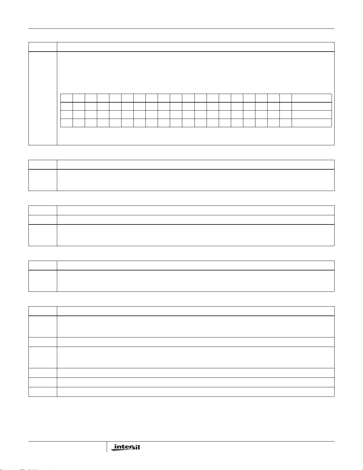
ISL5416
www.BDTIC.com/Intersil
TABLE 52. CHANNEL PROCESSING CONTROL (IWA = *001h) RESET STATE = 0x00000000h (Continued)
P(31:0) FUNCTION
2:0 AGC GAIN OUTPUT ROUNDING. The AGC gain is rounded to the selected number of bits. The AGC gain word into the rounder is:
E E E E M M M M M M M M M M M M M M.
The AGC gain is 2^E * (1.0 + M / 16384)
EEEE = 0 - 15, MMM...M = 0 - 16383
0 1. M M M M M M M M M M M M M M * 2^(E E E E)
TABLE 54.
FEDCBA9876543210 resolution
000=EE EEMMMMMMMMMMMM~ 96/65536dB
001=EE EEMMMMMMMMZ Z Z Z ~ 96/4096dB
010=EEEEMMMMZZZZZZZZ~ 96/256dB
Z = Zero
All other codes are reserved.
TABLE 55. NCO CENTER FREQUENCY (IWA = *002h) RESET STATE = 0x00000000h
P(31:0) FUNCTION
31:0 CARRIER CENTER FREQUENCY (CCF). The range is -Fs/2 to +Fs/2, where Fs is the input sample rate to the part. The carrier
frequency is: Fc = Fs * CCF / (2^32).
The CCF control is double buffered. The active carrier center frequency register is read at this address.
TABLE 56. NCO PHASE OFFSET (IWA = *003h) RESET STATE = 0x00000000h
P(31:0) FUNCTION
31:16 UNUSED.
15:0 PHASE OFFSET. This is the value of the phase offset added to the carrier NCO phase. This can be interpreted as either an unsigned
number with a range from 0 to 2π − (π / 32768) in 65536 steps, or as a signed number with a range of -π to π − (π / 32768) in 65536
steps.
TABLE 57. NCO CENTER FREQUENCY UPDATE (IWA = *004h) RESET STATE = INACTIVE
N/A FUNCTION
N/A STROBE. A write to this location generates a one-clock-wide strobe that transfers the carrier center frequency written to the holding
register (IWA = *002h) to the active register. The transfer can also be caused by a SYNCI signal (see IWA = *000h). The contents
of the active register are read at location IWA = *002h.
TABLE 58. NCO/MIXER/CIC CONTROL (IWA = *005h) RESET STATE = 0x00000000h
P(31:0) FUNCTION
31:29 MAXIMUM EXPONENT SHIFT SATURATION LEVEL. The maximum allowed shift factor from the input A/D range control block and
28 FORCE ZERO FEEDBACK. Set to 1 to force NCO phase accumulator feedback to 0. (Provided for test)
27 CLEAR FEEDBACK ON UPDATE.
26 RESERVED. Set to 0.
25:20 CIC BASE SHIFT FACTOR. The shift factor (exponents) from the input and the range control block are added to this value.
19 RESERVED. Set to 0.
the exponent from the input bus. If the sum exceeds this value, it will be saturated at this value. This is forced to 111 if the uP test
register is selected as the input source.
1 = clear NCO phase accumulator on frequency load/update (for synchronizing the NCO phase of multiple channels).
0 = phase continuous frequency updates.
50
Page 51

ISL5416
www.BDTIC.com/Intersil
TABLE 58. NCO/MIXER/CIC CONTROL (IWA = *005h) RESET STATE = 0x00000000h
P(31:0) FUNCTION
18:16 CIC STAGES. Number of CIC integrator/comb pairs (1-5). Stages are enabled starting with the largest accumulator.
000 = 1 stage;
001 = 2 stages;
010 = 3 stages;
011 = 4 stages;
100 = 5 stages;
Load with the number of stages minus 1.
15:0 CIC DECIMATION FACTOR. Load with (decimation - 1).
TABLE 59. PN GAIN (IWA = *006h) RESET STATE = 0x00000000h
P(31:0) FUNCTION
31:16 UNUSED.
15:0 PN LEVEL. Level of the PN generator data that is added to the mixer output when the PN generator is enabled in IWA = *001h, bit 16.
TABLE 60. FIR1, FIR2, POST-RESAMPLER CONTROL (IWA = *007h) RESET STATE = 0x00000000h
P(31:0) FUNCTION
31:19 UNUSED.
18:16 DECIMATION OF THE RESAMPLER DECIMATOR BLOCK. Load with the desired decimation factor minus one.
000 = Decimation of 1
111 = Decimation of 8
15 RESERVED. Set to 0.
14:12 FIR2 REQUIRED CLOCKS. This value should be set to: ceil (#TAPS/8) - 1.
11 RESERVED. Set to 0.
10:8 FIR2 DECIMATION. Available decimation through FIR2 block is 1-8. Set the value to: decimation factor - 1.
7 FIR1 ENABLE HBF MODE.
1 = Half Band Filter mode.
0 = normal mode.
6:4 FIR1 REQUIRED CLOCKS. Set to:
ceil (#TAPS/4) - 1.
3 RESERVED. Set to 0.
2:0 FIR1 DECIMATION. Available decimation through FIR1 block is 1-8. Set the value to: decimation factor - 1.
T ABLE 61. AGC CONTROL, MEAN/MEDIAN, DELAY, MODE (IWA = *008h) RESET STATE = 0x00000000h
P(31:0) FUNCTION
31:16 UNUSED.
15 RESERVED. Set to 0.
14 REAL TIME AGC GAIN OUTPUT SOURCE.
0 = the continuously updated loop filter output is provided to the output section as the “real time” AGC gain.
1 = the sampled loop filter output (sampled when the interval count is 0) is provided to the output section as the “real time” AGC gain.
13:8 DATA DELAY. This value is the number of samples that data is delayed to allow for AGC settling.
0x00 = no delay.
0x3F = 1 sample
. . .
0x01 = 63 samples.
7 LOOP GAIN 1 MEAN/MEDIAN.
1 = AGC settles to mean of the signal if LG1 is selected.
0 = AGC settles to median of the signal.
51
Page 52

ISL5416
www.BDTIC.com/Intersil
TABLE 61. AGC CONTROL, M EAN/ MED IAN, DELAY, MODE (IWA = *008h) RESET STATE = 0x00000000h (Continued)
P(31:0) FUNCTION
6 LOOP GAIN 2 MEAN/MEDIAN.
1 = AGC settles to mean of the signal if LG2 is selected.
0 = AGC settles to median of the signal.
5 uP LOOP GAIN SELECT. Set to:
1 = loop gain 2.
0 = loop gain 1.
4 uP LOOP GAIN CONTROL. Set to:
1 = uP loop gain select.
0 = counter controlled loop gain select.
3 DISABLE LOOP FILTER UPDATE. Set to:
1 = disable loop filter (holds the last value, the uP can load).
0 = normal AGC operation.
2 SAMPLED MODE.
1 = continuous forward gain updates.
0 = the forward gain held during the interval count (when loop gain 1 is used). The forward gain is continuously updated after the
interval count (when loop gain 2 is used).
1 ENABLE DELAY. Set to:
1 = enable delay
0 = no delay
NOTE: Delay must be enabled for Sampled Mode.
0 RESERVED. Set to 0.
TABLE 62. CONTROL BIT SETTINGS FOR AGC MODES
AGC MODE IWA=*001h IWA = *008h
BIT 20 BIT 4 BIT 2 BIT 1
CONTINUOUS UPDATE
µP controls loop gain
CONTIUOUS WITH DELAY 0 1 1 1
TIMED LOOP GAIN SELECTION 1 0 1 0
TIMED WITH DELAY 1 011
SAMPLED GAIN UPDATES
(always with delay)
TABLE 63. THRESHOLD (SET POINT) (IWA = *009h) RESET STATE = 0x00000000h
P(31:0) FUNCTION
31:16 UNUSED.
15:0 SET POINT. Bit weights:
2^
2 1 0. 1 2 3 4 5 6 7 8 9 0 1 2 3, 2
Note: There is a gain in the magnitude computation prior to the threshold compare. The gain versus number of clocks is:
CLOCKS GAIN
16 1.64676
8 1.647
4 1.642
3 1.630
2 1.581
The set point should be programmed to the desired level times the magnitude gain.
0
is the full scale vector magnitude on one axis before the magnitude computation gain is applied.
0 110
1 001
d
52
Page 53

ISL5416
www.BDTIC.com/Intersil
TABLE 64. UPPER/LOWER GAIN LIMIT (IWA = *00Ah) RESET STATE = 0x00000000h
P(31:0) FUNCTION
31:16 UPPER LIMIT.
E E E E M M M M M M M M M M M M
01.MMMMMMMMMMMM * 2^EEEE
Example: A gain of 48 (33.6 dB) would be:
5
or 0101100000000000
1.5 * 2
15:0 LOWER LIMIT. Same weighting as upper limit.
TABLE 65. LOOP GAINS (1 & 2) (IWA = *00Bh) RESET STATE = 0x00000000h
P(31:0) FUNCTION
31:24 ATTACK 1. Loop gain value used for increasing signal levels (decreasing gain). Bits 31:28 are the exponent, bits 27:24 are the
mantissa. Loop gain is 0.MMMM * 2
23:16 DECAY 1. Loop gain value used for decreasing signal levels (increasing gain).
15:8 ATTACK 2. Loop gain value used for increasing signal levels (decreasing gain). Bits 15:12 are the exponent, bits 11:8 are the
mantissa. Loop gain is 0.MMMM * 2
7:0 DECAY 2. Loop gain value used for decreasing signal levels (increasing gain).
TABLE 66. AGC COUNTER PRELOADS 1 (IWA = *00Ch) RESET STATE = 0x00000000h
P(31:0) FUNCTION
31:16 SLOT PERIOD (IN CLOCKS). Sets the timing interval (slot period) counter period. The interval counter can be reset by SYNCInX
(see IWA = *000h) to align it to the system timing. Load with number of clocks minus 1.
15:0 DELAY (In Clocks). Sets the delay from the start of the timing interval (bits (31:16 above) to the start of the interval set in IWA =
*00Dh. Load with number of clocks minus 1.
EEEE
. A loop gain of 00000000 weights the error by 2
EEEE
. A loop gain of 00000000 weights the error by 2
-19
to the input of the accumulator.
-19
to the input of the accumulator.
TABLE 67. AGC COUNTER PRELOADS 2 (IWA = *00Dh) RESET STATE = 0x00000000h
P(31:0) FUNCTION
31:16 UNUSED.
15:0 ADJUSTMENT INTERVAL (In Clocks). Sets the length of the adjustment period for timed AGC changes. (when loop gain 2 is used
in timed and sampled modes). Load with number of clocks minus 1.
TABLE 68. AGC uP GAIN LOAD VALUE (IWA = *00Eh) RESET STATE = 0x00000000h
P(31:0) FUNCTION
31:16 UNUSED.
15:0 GAIN. This location allows the uP to set the AGC gain directly. If the gain loaded by the uP is outside the limits set in IWA = *00Ah,
it will be set to the limit value. To set a fixed gain, set the loop gains to zero and the limits to full scale (or set both limits to the desired
gain). Bit weightings are the same as for the limits: EEEE MMMM MMMM MMMM.
TABLE 69. AGC uP GAIN LOAD STROBE (IWA = *00Fh) RESET STATE = INACTIVE
N/A FUNCTION
N/A STROBE. Writing to this location generates a strobe, synchronized to the clock, that updates the AGC with the gain value in register
N/A FUNCTION
N/A STROBE. Writing to this location copies the AGC loop filter accumulator contents to a holding register to stabilize it for reading by
IWA = *00Eh. The transfer can also be caused by a SYNCInX signal (see IWA = *000h).
TABLE 70. READBACK SAMPLE AGC GAIN AND MAGNITUDE (IWA = *010h) RESET STATE = INACTIVE
the uP at direct addresses 4 - 7. (The magnitude is read at this location after the strobe. Magnitude bit weightings are: 2
2
. . . 2
-13
)
53
Page 54

ISL5416
www.BDTIC.com/Intersil
TABLE 71. NCO 1 OUTPUT RATE -- TOP 32 BITS (IWA = *011h) RESET STATE = 0x00000000h
P(31:0) FUNCTION
31:0 RSout(48:16). This NCO sets the re-sampler output sample rate when the IHBF/Resampler block is enabled. If the HOIF is bypassed,
this is 2x the AGC (and FIR2) output rate. NOTE that the re-sampler only interpolates. The re-sampler output can be decimated using
a counter. The decimation is programmed in IWA = *007h, bits 18:16.
Fout = Fs * RSout / (2^48), where RSout = 0 to 2^48 -1, Fout = 0 to ~Fs.
Bits 48:16 of the active register are read back at this location.
must be
≤ F
If HOIF is enabled, then F
If IHBF is enabled, HOIF disabled, then F
TABLE 72. NCO 1 OUTPUT RATE -- LOWER 16 BITS (IWA = *012h) RESET STATE = 0x00000000h
P(31:0) FUNCTION
31:16 RSout(15:0). See IWA = *011h. Bits 15:0 of the active register are read back at this location.
15:0 UNUSED.
TABLE 73. NCO 2 INPUT RATE -- TOP 32 BITS (IWA = *013h) RESET STATE = 0x00000000h
P(31:0) FUNCTION
31:0 RSin(48:16). This NCO sets the output sample rate for the FIFO (input sample rate to the IHBF/Resampler block) when the
IHBF/Resampler block is enabled. If the HOIF is bypassed, this has no effect.
Fin = Fout * RSin / (2^48), where RSin = 0 to 2^48 -1, Fin = 0 to ~Fout.
Fin should be set equal to the output sample rate of FIR2 (Fs / (CICdeci * FIR1deci * FIR2deci)).
Bits 48:16 of the active register are read back at this location.
out
/2
CLK
must be ≤ F
out
CLK
TABLE 74. NCO 2 INPUT RATE -- LOWER 16 BITS (IWA = *014h) RESET STATE = 0x00000000h
P(31:0) FUNCTION
31:16 RSin(15:0). See IWA = *013.
15:0 UNUSED.
Bits 15:0 of the active register are read back at this location.
Register IWA = *015h is used to add delay to a channel. The output timing is unaffected (except at startup from reset). but the
group delay of the channel is adjusted. If the IHBF and HOIF are both enabled, the total delay range is 0 to 1023/256 FIR2 output
sample periods. NOTE: The HOIF can be enabled with no rate change by setting the NCO2 register (IWA = *013h and *014h) to
zero and setting the bit 22 of IWA = *001h.
TABLE 75. PHASE OFFSET (IWA = *015h) RESET STATE = 0x00000000h
P(31:0) FUNCTION
31:11 RESERVED. Set to 0.
10:9 FIFO DEPTH. After reset, the FIFO waits until it reaches a depth of 2 + this value (total of 2, 3, 4, or 5) before allowing FIFO reads.
7:0 RESAMPLER PHASE OFFSET. Allows the output sample timing to be shifted in increments of 1/256 the HOIF input period.
These bits can be used to add delay in increments of the FIR2 output sample rate.
HOIF or IHBF must be enabled.
8 HOIF INPUT DELAY.
1 = one HOIF input sample delay is added.
HOIF must be enabled.
00 = least delay.
FF = most delay.
HOIF must be enabled.
54
Page 55

ISL5416
www.BDTIC.com/Intersil
TABLE 76. LEAP COUNTER (IWA = *016h) RESET STATE = 0x00000000h
P(31:0) FUNCTION
31:0 LEAP COUNTER PRELOAD.
When the leap counter reaches zero, it resets the phase accumulators in NCO1 and NCO2 to zero (if enabled). Because some
frequencies cannot be represented exactly by the NCO control word, this function is provided to zero out any error that builds up due
to the limited NCO resolution. Load with the desired number of clocks between resets minus 1. Note that the ceiling function should
be used when computing the NCO frequency control words so that the NCOs build up a positive phase error and phase accumulator
carries are not suppressed.
TABLE 77. RESAMPLER FREQUENCY/PHASE UPDATE STROBE (IWA = *017h) RESET STATE = INACTIVE
N/A FUNCTION
N/A STROBE. A write to this location transfers the contents of IWA = *011/*012h and IWA = *013/*014h holding registers to the active
N/A FUNCTION
N/A SOFT RESET. A write to this location generates a soft reset of the channel. This clears the slave registers of master/slave pairs and
N/A FUNCTION
N/A STROBE. A write to this location updates the active data path control register from its holding register. The transfer can also be
resampler NCO frequency registers. The transfer can also be caused by a SYNCInX signal (see IWA = *000h).
TABLE 78. CHANNEL SOFT RESET (IWA = *018h) RESET STATE = INACTIVE
stops processing in the channel.
TABLE 79. UPDATE DATA PATH CONTROL REGISTER (IWA = *019h) RESET STATE = INACTIVE
caused by a SYNCInX signal (see IWA = *000h). The active register is cleared on reset, disabling channel processing, so this update
is used to synchronously start the channel processing.
TABLE 80. ADVANCE (IWA = *01Ah) RESET STATE = INACTIVE
N/A FUNCTION
N/A STROBE. A write to this location repeats one sample at the output of the CIC. Should only be used if there is sufficient overhead for
processing an extra sample.
Locations IWA = *01A and *01B delete or repeat a sample at
the input to FIR1 to shift the system timing. These locations
should not be used if the IHBF or re-sampler is enabled.
TABLE 81. RETARD (IWA = *01Bh) RESET STATE = INACTIVE
N/A FUNCTION
N/A STROBE. A write to this location deletes one sample at the output of the CIC.
TABLE 82. FIR 1 COEFFICIENTS (32 x 20) (IWA = *100h THRU *11Fh) RESET STATE = INACTIVE
P(31:0) FUNCTION
31:20 UNUSED.
19:0 COEFFICIENTS. Twos complement -524287 to +524287 (-524288 not allowed). +524288 would be unity gain.
TABLE 83. FIR 2 COEFFICIENTS (64 x 20) (IWA = *200h THRU *23Fh) RESET STATE = UNDEFINED
P(31:0) FUNCTION
31:20 UNUSED.
19:0 COEFFICIENTS. Twos complement -524287 to +524287 (-524288 not allowed). +524288 would be unity gain.
55
Page 56

s
e
ISL5416
www.BDTIC.com/Intersil
TABLE 83. FIR 2 COEFFICIENTS (64 x 20) (IWA = *200h THRU *23Fh) RESET STATE = UNDEFINED
P(31:0) FUNCTION
Each multiplier has up to 8 coefficients. If the six bit coefficient addresses are labeled M2 M1 M0 C2 C1 C0, where the M-bit
select the multiplier (000 is the first multiplier encountered by the data samples), and the C-bi ts select the coefficient (00 0 is th
first coefficient encountered by the data samples). M2 is not used for FIR1.
For example, if an eight tap filter is used for FIR1, the coefficients would be loaded:
(earliest)
C0 --- 000000 (*100h)
C1 --- 000001
C2 --- 001000
C3 --- 001001
C4 --- 010000
C5 --- 010001
C6 --- 011000
C7 --- 011010 (*11Ah)
When the Half Band Filter mode is enabled for FIR1, the zero valued zero crossing coefficients are not loaded, but the
coefficients must be centered around the hard wired center tap. This means that zeros valued coefficients must be added if the
number of coefficients per multiplier is not uniform. For example, with an 11-tap Half Band Filter with coefficients:
C0, 0, C1, 0, C2, 0.5, C3, 0, C4, 0, C5,
the coefficient loading would be:
0 ----- 000000 (*100h)
C0 --- 000001
C1 --- 001000
C2 --- 001001
C3 --- 010000
C4 --- 010001
C5 --- 011000
0 ----- 011001 (*119h)
The filter computation requires two clock cycles for the computation. Due to the added zero-valued coefficients, the group delay
has increased from 6 to 8 sample periods.
56
Page 57

ISL5416
www.BDTIC.com/Intersil
Absolute Maximum Ratings Thermal Information
Supply Voltage. . . . . . . . . . . . . . . . . . . . . . . . . . . . . . . . . . 2.5 (core)
4.6 (I/O’s)
Input, Output or I/O Voltage. . . . . . . . . . . . . . . . .GND -0.5V to 5.5V
ESD Classification . . . . . . . . . . . . . . . . . . . . . . . . . . . . . . . . . Class I
Operating Conditions
Voltage Range I/O, V
Voltage Range core, V
Temperature Range
Industrial. . . . . . . . . . . . . . . . . . . . . . . . . . . . . . . . . -40
Input Low Voltage . . . . . . . . . . . . . . . . . . . . . . . . . . . . . 0V to +0.8V
Input High Voltage . . . . . . . . . . . . . . . . . . . . . . . . . . 2V to I/O V
CAUTION: Stresses above those listed in “Absolute Maximum Ratings” may cause permanent damage to the device. This is a stress only rating and operation of the
device at these or any other conditions above those indicated in the operational sections of this specification is not implied.
NOTE: NOTE: θJA is measured with the component mounted on a high effective thermal conductivity test board with “direct attach” features in free
air or with the airflow. See Tech Brief TB379 for details
. . . . . . . . . . . . . . . . .+3.135V to +3.465V
CCIO
. . . . . . . . . . . . . . . . . .+1.71V to +1.89V
CCC
o
C to 85oC
CCIO
Thermal Resistance (Typical) θJA (oC/W)
256 Lead BGA Package. . . . . . . . . . . . . . . . . . . . . . 31
w/200 LFM Air Flow . . . . . . . . . . . . . . . . . . . . . . . . . 28
w/400 LFM Air Flow . . . . . . . . . . . . . . . . . . . . . . . . . 26
Maximum Junction Temperature . . . . . . . . . . . . . . . . . . . . . . .150
Maximum Storage Temperature Range. . . . . . . . . . -65
For recommended soldering conditions see Tech Brief 334.
o
C to 150oC
o
C
Electrical Specifications V
PARAMETER SYMBOL TEST CONDITIONS MIN TYPICAL MAX UNITS
Logical One Input Voltage V
Logical Zero Input Voltage V
Output High Voltage V
Output Low Voltage V
Input Leakage Current I
Output Leakage Current I
Standby Power Supply Current
(core)
Standby Power Supply Current
(IO’s)
Operating Power Supply Current
(core)
Operating Power Supply Current
(IO’s)
Operating Power Supply Core
Current (typical)
Input Capacitance C
CCC
I
CCSB-CRVCCC
I
CCSB-IOVCCC
I
CCOP-CR
I
CCOP-IO
I
CCOP-TYP
= Core supply: 1.8V ± 0.09V, TA = -40oC to 85oC, Industrial
V
IH
IL
OH
OL
I
O
IN
= 3.45V 2.0 V
CCIO
V
= 3.15V 0.8 V
CCIO
IOH = -2mA, V
IOL = 2mA, V
VIN = V
CCIO
VIN = V
CCIO
= 1.89V, See AC Test load circuit, No
CLK
= 1.89V, See AC Test load circuit,
No CLK
f = 80MHz, VIN = V
V
= 1.89V, See AC Test load circuit,
CCC
f = 80MHz, VIN = V
= 1.89V, See AC Test load circuit,
V
CCC
f = 80MHz, VIN = V
= 1.89V, See AC Test load circuit,
V
CCC
Freq = 1MHz, V
are referenced to device ground
= 3.15V 2.6 3 V
CCC
= 3.15V 0.1 0.4 V
CCC
or GND, V
or GND, V
CCC
CCC
CCC
open, all measurements
CCC
= 3.465V -10 < 1
CCIO
= 3.465V -10 10 µA
CCIO
or GND,
or GND,
or GND,
(NOTE 3)
500
(NOTE 1, 4)
10 µA
12
(NOTE 6)
0.75 mA
660 mA
150 mA
5pF
mA
mA
(Note 2)
Output Capacitance C
NOTES:
1. Power Supply current is proportional to frequency of operation and programmed configuration of the part. Typical rating for I
2. Capacitance: T
process or design changes.
3. Typical Pull-up/down resistance values are 60 kΩ.
4. Typical measured power on the Evaluation board:
•. UMTS: CLK = 76.8 MHz, Total Power = 1.1 W (core current = 500 mA; I/O current = 60 mA)
•. CDMA2000: CLK = 80 MHz, Total Power = 750 mW (core current = 360 mA; I/O current = 30 mA).
= 25oC, controlled via design or process parameters and not directly tested. Characterized upon initial design and at major
A
OUT
57
5pF
(Note 2)
is 6.5 mA/MHz.
CCOP
Page 58

ISL5416
www.BDTIC.com/Intersil
Electrical Specifications V
INPUT AND CONTROL TIMING, CLOCK SKEW (FIGURE 11 AND 12)
CLKC Frequency f
CLKC High t
CLKC Low t
Setup Time - Data Inputs, Input Enables to CLKX High t
Hold Time - Data Inputs, Input Enables to CLKX High t
Setup Time - SYNCInX to CLKC High t
Hold Time - SYNCInX to CLKC High t
CLKC to Output Valid - SYNCO t
Pulse Width Low t
RESET
Setup Time to CLKC High (Note 5) t
RESET
CLKX to CLKC skew 1 (FIGURE 12) t
CLKX to CLKC skew 2 (FIGURE 12) t
MICROPROCESSOR WRITE TIMING (µP mode = 0, FIGURE 13)
P(15:0) Setup Time to Rising Edge of WR
P(15:0) Hold Time from Rising Edge of WR
A(2:0) Setup Time to Rising Edge of WR
A(2:0) Hold Time from Rising Edge of WR
Setup Time to Rising Edge of WR t
CE
Hold Time from Rising Edge of WR t
CE
Low Time t
WR
MICROPROCESSOR READ TIMING (µP mode = 0, FIGURE 14)
A(2:0) Hold Time from RISING Edge of RD
A(2:0) to P(15:0) Data Valid Time t
Enable Time t
RD
Disable Time (Note 6) t
RD
Setup Time to Falling Edge of RD t
CE
Hold Time from Rising Edge of RD (Note 6) t
CE
READ Cycle Time (Note 7) t
MICROPROCESSOR WRITE TIMING (µP MODE = 1, FIGURE 15)
P(15:0) Setup Time to Rising Edge of DSTRB
P(15:0) Hold Time from Rising Edge of DSTRB
A(2:0) Setup Time to Rising Edge of DSTRB
A(2:0) Hold Time from Rising Edge of DSTRB
Setup Time to Rising Edge of DSTRB t
CE
Hold Time from Rising Edge of DSTRB t
CE
Setup Time to Falling Edge of DSTRB t
R/W
Hold Time from Rising Edge of DSTRB t
R/W
Low Time t
DSTRB
MICROPROCESSOR READ TIMING (µP MODE = 1, FIGURE 16)
A(2:0) Hold Time from RISING Edge of DSTRB
A(2:0) to P(15:0) Data Valid Time t
= Core supply: 1.8V ± 0.09V, V
CCC
PARAMETER SYMBOL MIN MAX UNITS
(Note 7) t
t
(Note 7) t
= IO’s supply: 3.3V ± 0.165V, TA = -40oC to 85oC Industrial
CCIO
CLK
CH
CL
DS
DH
SYNCS
SYNCH
PDC
RW
RS
CKS1
CKS2
t
PSW
t
PHW
t
ASW
t
AHW
CSW
CHW
WPWL
AHR
DV
RE
RD
CSF
CHR
RCY
t
PSR
t
PHR
t
ASR
AHR
CSR
CHR
R/WSF
R/WHR
DW
AHR
DV
-95MHz
3-ns
4-ns
5.5 - ns
0-ns
3
0
-5ns
5-ns
5-ns
2.5
2.5
7.5 - ns
-1 - ns
8.5 - ns
-2 - ns
7-ns
-2 - ns
5-ns
-4 - ns
-19ns
-8.5ns
-6ns
2.5 - ns
0-ns
25 - ns
8-ns
-0.5 - ns
7.5 - ns
-1.5 - ns
8-ns
-2 - ns
0-ns
-1 - ns
6-ns
-1 - ns
-16ns
58
Page 59

ISL5416
www.BDTIC.com/Intersil
Electrical Specifications V
= Core supply: 1.8V ± 0.09V, V
CCC
= IO’s supply: 3.3V ± 0.165V, TA = -40oC to 85oC Industrial
CCIO
PARAMETER SYMBOL MIN MAX UNITS
DSTRB Enable Time t
Disable Time (Note 6) t
DSTRB
Setup Time to Falling Edge of DSTRB t
CE
Hold Time from Rising Edge of DSTRB (Note 7) t
CE
Low Time t
DSTRB
READ Cycle Time (Note 8) t
RE
RD
CSF
CHR
DW
RCY
-14ns
-6.5ns
7.5 - ns
-2 - ns
5-ns
25 ns
JTAG TIMING (FIGURE 17)
TDI, TMS Set Up TS
TDI, TMS Hold TH
TCLK TO TDO VALID TOV
TCLK TO TDO DISABLED TOD
TCLK TO TDO ENABLED TOE
CAPTURE INPUT SETUP TIME t
CAPTURE INPUT HOLD TIME t
TCLK TO OUTPUT VALID (Note 6) t
DVLD
TT
TT
TDO
TDO
TDO
ISTP
IHLD
4.5 ns
1.5 ns
7ns
7ns
7ns
5ns
1.5 ns
26ns
CLOCK OUTPUT TIMING AND OUTPUT ENABLES (FIGURE 18)
CLKC to Parallel Data, FSYNCX and CLKO1 (Divide-by 2 thru 16 Modes) t
CLKC Low to CLKO1 Low (Divide-by 1 Mode) t
CLKC High to CLKO1 High (Divide-by 1 Mode) t
PD
PDL
PDH
2
(NOTE 6)
2
(NOTE 6)
2
6.5 ns
6.5 ns
6.5 ns
(NOTE 6)
Time Skew Between CLKO1 and Parallel Data or FSYNCX (Divide-by 2 thru 16 Modes) t
Time Skew Between CLKO1 and Parallel Data or FSYNCX (Divide-by 1 Mode) t
OUTPUT ENABLE TIME t
OUTPUT DISABLE TIME t
SKEW3
SKEW4
OEN
ODIS
-1.5 1.5 ns
-2.5 1.5 ns
6ns
4ns
NOTES:
5. The ISL5416 goes into reset immediately on RESET
going low and comes out of reset on the 4th rising edge of CLK after RESET goes high.
6. Controlled via design or process parameters and not directly tested. Characterized upon initial design and at major process or design changes.
7. t
AHR
and t
apply ONLY to direct reads of addresses 4 - 7.
CHR
8. Reading from direct addresses 4 - 7 (Sequential Read Mode).
AC Test Load Circuit
C
(NOTE)
L
S
1
EQUIVALENT CIRCUIT
DUT
NOTE - TEST HEAD CAPACITANCE, 50pF (TYP)
SWITCH S1 OPEN FOR I
CCSB
AND I
CCOP
59
±
I
OH
1.5V I
OL
Page 60
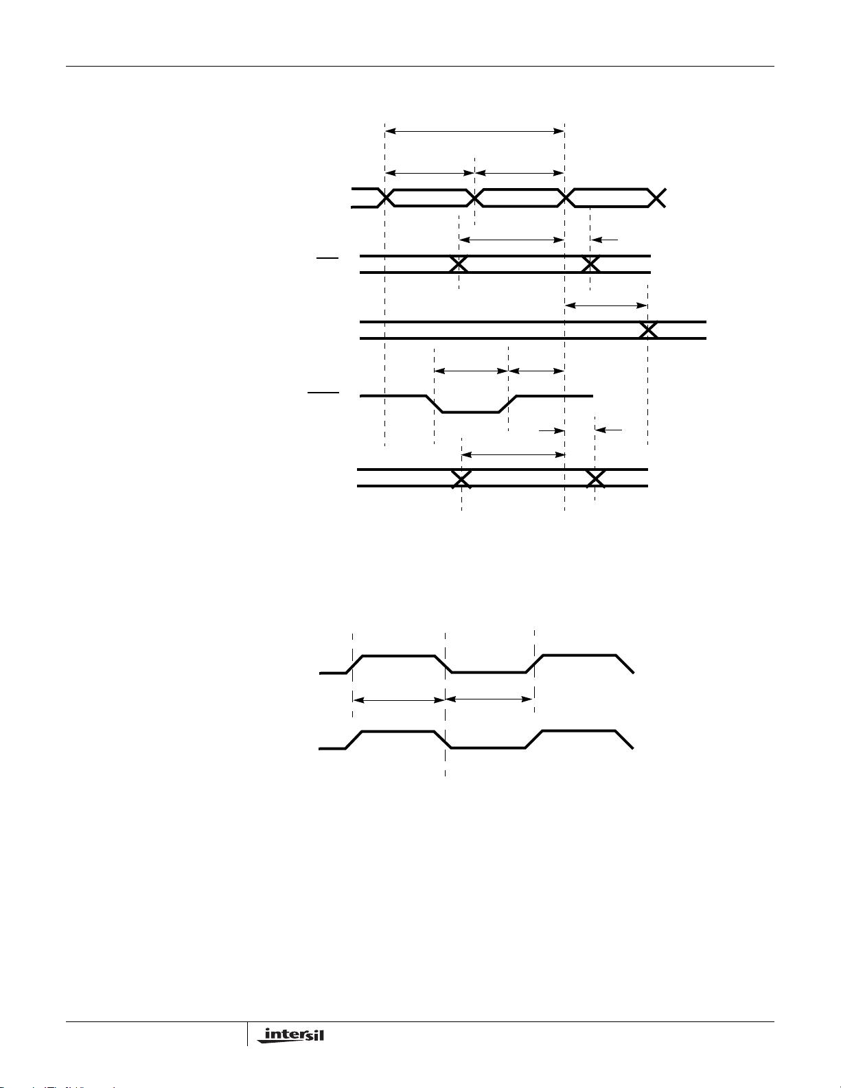
Waveforms
www.BDTIC.com/Intersil
ISL5416
1/f
CLKC
CLKC
Xin, ENIX
XOUT, SYNCO
RESET
SYNCInX
X = A, B, C or D
LOW to HIGH edge for active HIGH clock
HIGH to LOW edge for active LOW clock
t
CH
t
RW
t
CL
t
DS
t
SYNCS
t
DH
t
PDC
t
RS
t
SYNCH
X = A, B, C or D
CLKX
CLKC
FIGURE 11. CONTROL TIMING
t
CKS2
FIGURE 12. CLOCK SKEWS
t
CKS1
60
Page 61
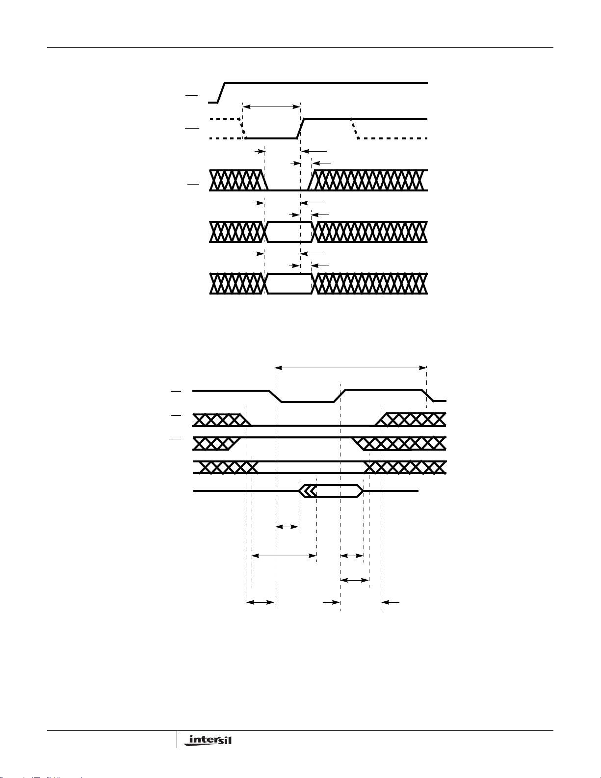
Waveforms (Continued)
www.BDTIC.com/Intersil
ISL5416
RD
t
WPWL
WR
t
CSW
t
CHW
CS
t
ASW
t
AHW
A<2:0>
P<15:0>
FIGURE 13. MICROPROCESSOR WRITE TIMING (µP mode = 0)
VALID
VALID
t
PSW
t
PHW
t
RCY
RD
CE
WR
ADD(2:0)
P(15:0)
t
RE
t
DV
t
CSF
FIGURE 14. MICROPROCESSOR READ TIMING (µP mode = 0)
t
RD
t
AHR
t
CHR
61
Page 62

Waveforms (Continued)
www.BDTIC.com/Intersil
ISL5416
CE
RD/WR
ADD(2:0)
P(15:0)
DSTRB
t
DW
t
R/WSF
t
PSR
t
CSR
t
ASR
FIGURE 15. MICROPROCESSOR WRITE TIMING (µP mode = 1))
t
PHR
t
AHR
t
CHR
t
R/WHR
CE
RD/WR
ADD(2:0)
P(15:0)
DSTRB
t
RCY
t
RE
t
t
CSF
t
RWSF
DV
t
DW
t
AHR
t
CHR
t
RD
FIGURE 16. MICROPROCESSOR READ TIMING (µP mode = 1))
62
Page 63

Waveforms (Continued)
www.BDTIC.com/Intersil
INPUTS
(CAPTURE)
TCLK
ISL5416
t
ISTPtIHLD
TDI, TMS
TDO
OUTPUTS
TOV
TDO
t
DVLD
TS
FIGURE 17. JTAG TIMING
TT
TH
TT
TOD
TDO
TOE
TDO
63
Page 64

Waveforms (Continued)
www.BDTIC.com/Intersil
ISL5416
CLKC
CLKO1
(/2 THRU /16)
FSYNCX
AOUT, BOUT, COUT, DOUT,
EOUT
OEX
XOUT
t
OEN
t
SKEW3
t
PD
CLKO1
(DIVIDE BY 1)
t
ODIS
t
PDH
t
SKEW4
t
PDL
FIGURE 18. OUTPUT TIMING
64
Page 65

ISL5416
www.BDTIC.com/Intersil
TABLE 84. CIC PASSBAND AND ALIAS LEVELS
FREQUENCY 5TH ORDER 4TH ORDER 3RD ORDER 2ND ORDER 1ST ORDER
/ R PASSBAND ALIAS PASSBAND ALIAS PASSBAND ALIAS PASSBAND ALIAS PASSBAND ALIAS
f
S
0 0<-2000<-2000<-2000<-2000<-200
0.01 -0.007 -199.564 -0.006 -159.651 -0.004 -119.738 -0.003 -79.825 -0.001 -39.913
0.02 -0.029 -169.041 -0.023 -135.233 -0.017 -101.425 -0.011 -67.617 -0.006 -33.808
0.03 -0.064 -151.023 -0.051 -120.818 -0.039 -90.614 -0.026 -60.409 -0.013 -30.205
0.04 -0.114 -138.129 -0.091 -110.503 -0.069 -82.877 -0.046 -55.252 -0.023 -27.626
0.05 -0.179 -128.048 -0.143 -102.438 -0.107 -76.829 -0.071 -51.219 -0.036 -25.610
0.06 -0.257 -119.749 -0.206 -95.799 -0.154 -71.849 -0.103 -47.900 -0.051 -23.950
0.07 -0.351 -112.683 -0.280 -90.146 -0.210 -67.610 -0.140 -45.073 -0.070 -22.537
0.08 -0.458 -106.522 -0.367 -85.218 -0.275 -63.913 -0.183 -42.609 -0.092 -21.304
0.09 -0.580 -101.054 -0.464 -80.843 -0.348 -60.633 -0.232 -40.422 -0.116 -20.211
0.10 -0.717 -96.135 -0.573 -76.908 -0.430 -57.681 -0.287 -38.454 -0.143 -19.227
0.11 -0.868 -91.662 -0.694 -73.330 -0.521 -54.997 -0.347 -36.665 -0.174 -18.332
0.12 -1.034 -87.558 -0.827 -70.047 -0.620 -52.535 -0.413 -35.023 -0.207 -17.512
0.13 -1.214 -83.766 -0.971 -67.013 -0.728 -50.260 -0.486 -33.507 -0.243 -16.753
0.14 -1.409 -80.241 -1.127 -64.193 -0.846 -48.145 -0.564 -32.096 -0.282 -16.048
0.15 -1.619 -76.947 -1.295 -61.558 -0.972 -46.168 -0.648 -30.779 -0.324 -15.389
0.16 -1.844 -73.855 -1.475 -59.084 -1.107 -44.313 -0.738 -29.542 -0.369 -14.771
0.17 -2.084 -70.943 -1.667 -56.754 -1.251 -42.566 -0.834 -28.377 -0.417 -14.189
0.18 -2.340 -68.189 -1.872 -54.551 -1.404 -40.913 -0.936 -27.276 -0.468 -13.638
0.19 -2.610 -65.579 -2.088 -52.463 -1.566 -39.347 -1.044 -26.231 -0.522 -13.116
0.20 -2.896 -63.098 -2.317 -50.478 -1.737 -37.859 -1.158 -25.239 -0.579 -12.620
0.21 -3.197 -60.734 -2.558 -48.587 -1.918 -36.440 -1.279 -24.294 -0.639 -12.147
0.22 -3.514 -58.477 -2.811 -46.782 -2.108 -35.086 -1.406 -23.391 -0.703 -11.695
0.23 -3.847 -56.319 -3.077 -45.055 -2.308 -33.792 -1.539 -22.528 -0.769 -11.264
0.24 -4.195 -54.252 -3.356 -43.402 -2.517 -32.551 -1.678 -21.701 -0.839 -10.850
0.25 -4.560 -52.269 -3.648 -41.815 -2.736 -31.361 -1.824 -20.907 -0.912 -10.454
0.26 -4.941 -50.363 -3.953 -40.291 -2.965 -30.218 -1.976 -20.145 -0.988 -10.073
0.27 -5.338 -48.531 -4.271 -38.825 -3.203 -29.119 -2.135 -19.412 -1.068 -9.706
0.28 -5.752 -46.767 -4.602 -37.413 -3.451 -28.060 -2.301 -18.707 -1.150 -9.353
0.29 -6.183 -45.066 -4.946 -36.053 -3.710 -27.040 -2.473 -18.026 -1.237 -9.013
0.30 -6.631 -43.426 -5.305 -34.740 -3.978 -26.055 -2.652 -17.370 -1.326 -8.685
0.31 -7.096 -41.842 -5.677 -33.473 -4.257 -25.105 -2.838 -16.737 -1.419 -8.368
0.32 -7.578 -40.311 -6.063 -32.249 -4.547 -24.187 -3.031 -16.125 -1.516 -8.062
0.33 -8.078 -38.832 -6.463 -31.066 -4.847 -23.299 -3.231 -15.533 -1.616 -7.766
0.34 -8.596 -37.401 -6.877 -29.921 -5.158 -22.440 -3.439 -14.960 -1.719 -7.480
0.35 -9.133 -36.015 -7.306 -28.812 -5.480 -21.609 -3.653 -14.406 -1.827 -7.203
0.36 -9.688 -34.674 -7.750 -27.739 -5.813 -20.804 -3.875 -13.869 -1.938 -6.935
0.37 -10.262 -33.374 -8.209 -26.699 -6.157 -20.024 -4.105 -13.349 -2.052 -6.675
0.38 -10.854 -32.114 -8.684 -25.691 -6.513 -19.268 -4.342 -12.845 -2.171 -6.423
0.39 -11.467 -30.892 -9.174 -24.713 -6.880 -18.535 -4.587 -12.357 -2.293 -6.178
0.40 -12.099 -29.707 -9.679 -23.766 -7.260 -17.824 -4.840 -11.883 -2.420 -5.941
0.41 -12.752 -28.557 -10.201 -22.846 -7.651 -17.134 -5.101 -11.423 -2.550 -5.711
0.42 -13.425 -27.442 -10.740 -21.953 -8.055 -16.465 -5.370 -10.977 -2.685 -5.488
0.43 -14.119 -26.359 -11.295 -21.087 -8.472 -15.815 -5.648 -10.544 -2.824 -5.272
0.44 -14.835 -25.308 -11.868 -20.246 -8.901 -15.185 -5.934 -10.123 -2.967 -5.062
0.45 -15.573 -24.287 -12.458 -19.430 -9.344 -14.572 -6.229 -9.715 -3.115 -4.857
0.46 -16.333 -23.296 -13.066 -18.637 -9.800 -13.978 -6.533 -9.318 -3.267 -4.659
0.47 -17.116 -22.334 -13.693 -17.867 -10.270 -13.400 -6.847 -8.933 -3.423 -4.467
0.48 -17.923 -21.399 -14.339 -17.119 -10.754 -12.840 -7.169 -8.560 -3.585 -4.280
0.49 -18.754 -20.492 -15.003 -16.393 -11.253 -12.295 -7.502 -8.197 -3.751 -4.098
0.50 -19.610 -19.610 -15.688 -15.688 -11.766 -11.766 -7.844 -7.844 -3.922 -3.922
65
Page 66

ISL5416
www.BDTIC.com/Intersil
TABLE 85. ISL5416 RANGE CONTROL BIT WEIGHTING
GFEDCBA9876543210.123456789ABCDEF
INPUT SXXXXXXXXXXXXXXX
DC OFFSET SXXXXXXXXXXXXXXX
MAGNITUDE 0000000000000000XXXXXXXXXXXXXXXX
IMMEDIATE
THRESHOLD
ACCUMULATOR 0 X X X XXXXXXXXXXXXXXXXXXXXXXXXXXXX
SHIFT:
0000 XXXXXXXXXXXXXXXX
0001 XXXXXXXXXXXXXXXX
0010 X XXXXXXXXXXXXXXX
0011 X X XXXXXXXXXXXXXX
0100 X X X XXXXXXXXXXXXX
0101 XXXXXXXXXXXXXXXX
0110 XXXXXXXXXXXXXXXX
0111 X XXXXXXXXXXXXXXX
1000 X X XXXXXXXXXXXXXX
1001 X X X XXXXXXXXXXXXX
1010 XXXXXXXXXXXXXXXX
1011 XXXXXXXXXXXXXXXX
1100 X XXXXXXXXXXXXXXX
1101 X X XXXXXXXXXXXXXX
1110 X X X XXXXXXXXXXXXX
1111 0 X X X XXXXXXXXXXXX
SHIFTER OUTPUT XXXXXXXXXXXXXXXX
THRESHOLD 1,
THRESHOLD 2
dB VALUE 24 12 6
GAIN
ACCUMULATOR
uP DELTA
PROGRAMMED
Max Delta = 12 dB
DELTA3 (LOWER) 111XXXXXXXXXXXXXX (accumulator + DELTA 1)
DELTA 2 (UPPER) 0 0 0 X XXXXXXXXXXXXX (accumulator + DELTA 2)
DELTA 1 (IMMED.) 000XXXXXXXXXXXXXX (accumulator + DELTA 3)
uP LOAD BITS 0XXXXXXXXXXXXXXXX
LEAK SSXXXXXXXXXXXXXXX (accumulator + leak)
MSB is sign extended
LIMITS 0XXX
TO MAPPING LUT X X X
0XXXXXXXXXXXXXXXX
XXXXXXXXXXXXXX (14 bits)
XXXXXXXXXXXXXXXX
→
→
XXXXXXXXXXXXXXXX
TABLE 86. AGC BIT WEIGHTS
AGC BIT
WEIGHTS FEDCBA9 8 7 6 5432 10. 12345678901234567890123456789
FORWARD
GAIN PATH
INPUTS I/Q
S.12345678901234567890123
66
Page 67

ISL5416
www.BDTIC.com/Intersil
TABLE 86. AGC BIT WEIGHTS (Continued)
AGC BIT
WEIGHTS FEDCBA9 8 7 6 5432 10. 12345678901234567890123456789
BARREL SHIFTER SHIFT
EEEE = 0 S.12345678901234567890123
EEEE = 4 S.12345678901234567890123GGGG
EEEE = 8 S.12345678901234567890123GGGGGGGG
EEEE = 15 S.12345678901234567890123GGGGGGGGGGGGGGG
------------SATURATE ON OVERFLOW---------
BS OUT /
MULT IN
MULT
1.0 <= M<= 2.0
MULT OUT S012345678901234567890123
SATURATE BASED ON SHIFT AND MULT OUT:
FEEDBACK
PATH;
OUTPUTS I/Q
MAG IN S.12345678901234567890123
MAGNITUDE (G = 1.647, MAX IN = 1.414, MAX OUT = 2.33):
THRESHOLD 2101234567890123
MEAN ERROR S101234567890123
MEDIAN
ERROR
LG MANTISSA G.1234
LG MANT
MULT OUT
LG EXP SHIFT
= 0
LG EXP SHIFT
= 4
LG EXP SHIFT
= 8
LG EXP SHIFT
= 15
LG ACCUM 3 2 1 0. 12345678901234567890123456789
LL / UL GGG0123456789012345
OUTPUT FWD
GAIN
OUTPUT uP /
PARALLEL
BIT WEIGHTS (dB); MAX GAIN = 96.3293 dB
S = SIGN ..................
G = LOGIC 0 1 00005731000000000
E=EXPONENT 684210578942100000
M =
MANTISSA
V = LOGIC 1 842631531105799574
-S.12345678901234567890123
GV12345678901234
S.12345678901234567890123
G1012345678901234567890123
GGG.VGGGGGGGGGGGG
VVV.VGGGGGGGGGGGG
S10123456789012345
SSSSSSSSSSSSSSSSS1012345678901234
SSSSSSSSSSSSS10123456789012345GGG
SSSSSSSSS10123456789012345GGGGGGG
SS10123456789012345GGGGGGGGGGGGGG
E EEEMMMMMMMMMMMMMM
GE EEEMMMMMMMMMMM
421
842631000000000000
421005268473152100
67
Page 68

ISL5416
www.BDTIC.com/Intersil
0.0
-1.0
-2.0
-3.0
dB
-4.0
-5.0
-6.0
0.0 0.1 0.2 0.3 0.4 0.5
N = 5
N = 4
/R
f
S
N = 1
N = 2
N = 3
FIGURE 19. CIC PASSBAND ROLLOFF (N = # OF STAGES,
R = DECIMATION FACTOR, f
OUTPUT RATE)
0
N = 1
-20
-40
-60
dB
-80
-100
-120
-140
0.00 0.10 0.20 0.30 0.40 0.50
N = 4
N = 5
N = 2
N = 3
f
/R
S
/R = 1 is CIC
S
FIGURE 19A. CIC FIRST ALIAS LEVEL (N = # OF STAGES,
R = DECIMATION FACTOR, f
OUTPUT RATE)
/R = 1 is CIC
S
0
-2 0
-4 0
-6 0
-8 0
-100
-120
-140
-160
-180
0 1 2 3 4 5 6
FIGURE 20. A TYPICAL CARRIER NCO SPECTRUM
PLOT (65536 POINT FFT, BLACKMAN WINDOW,
800 Hz BIN NBW (29 dB). PEAK BIN IS AT -132
dBc, NOISE FLOOR AT -190 dBc/Hz.
x 1 0
4
0
-20
-40
-60
dB
-80
-100
-120
-140
0.0 0.5 1.0 1.5 2.0 2.5
/R
f
S
3.0
FIGURE 19B. 5TH ORDER (N = 5) CIC RESPONSE
(R = DECIMATION FACTOR, f
/R = 1 is CIC
S
68
Page 69

ISL5416
www.BDTIC.com/Intersil
Data Sheet Revisions:
TABLE 87. REVISION HISTORY
REVISION DATE DESCRIPTION
6006.2 January 10, 2003 - TRST
CDMA2000-1XRTT:
Figure below shows the o verall response using 5-stage CIC filter ,
32-tap first FIR filter bloc k an d 64-tap second FIR filter b loc k.
Pin Description text added for Circuit Board schematics
- Added text in the VGA/RF Attenuator (Range Control) section, last paragraph
- Figure 3, “NCO, Mixer and CIC Block Diagram”, corrected FIR coefficients table
- Figure 4, “FIR1 and FIR2 Block Diagrams”, updated
- Added Power-up Sequencing Explanation on Page 27
- Table 24, IWA = 0*01h, updated register description (bit values remained the same)
- Table 51, IWA = *000h, updated register description (bit values remained the same)
- Table 52, IWA = *001h, bits 31:29, updated description (bit values remained the same)
- Table 52, IWA = *001h, bits 2:0, updated description (bit values remained the same)
- Table 61, IWA = *008h, bit 0 changed to “RESERVED, Set to 0”
- Table 62, “Control Bit Settings for AGC Modes” added
- Table 83, Added the FIR coefficient loading procedure at the bottom of the table
- In Electrical Specifications table added the following values: t
- Figure 12, “Clock Skews”, updated
- Added package drawing note (last page)
CHR
, t
RCY
, t
DW
-20
-40
-60
-80
-100
-120
1 2 3 4 5 6 7 8 9 10
FIGURE 21. OVERALL FILTER RESPONSE OF A SINGLE CDMA2000 CHANNEL
x 10
6
69
Page 70

UMTS / W-CDMA:
www.BDTIC.com/Intersil
Figure below shows the overall response using 5-stage CIC
filter, 32-tap first FIR filter block and 64-tap second FIR filter
block.
0
-20
-40
-60
-80
ISL5416
-100
0.5 1 1.5 2 2.5 3
FIGURE 22. OVERALL FILTER RESPONSE OF A SINGLE UMTS CHANNEL
x 10
7
70
Page 71

Plastic Ball Grid Array Packages (BGA)
www.BDTIC.com/Intersil
o
CORNER I.D.
CORNER
0.15
M A BC
0.006
0.08
M
0.003
S
A
C
A1
D
A1
TOP VIEW
C
b
A
A1
1516
A2
D1
81314 12 11 10 9
765 342
S
A
BOTTOM VIEW
SIDE VIEW
ALL ROWS AND COLUMNS
A
E
B
A1
1
CORNER I.D.
A
B
C
D
E
F
G
H
E1
J
K
L
M
N
P
R
T
e
bbb
SEATING PLANE
A1
CORNER
C
aaa
C
ISL5416
V256.17x17
256 BALL PLASTIC BALL GRID ARRAY PACKAGE
INCHES MILLIMETERS
SYMBOL
A - 0.059 - 1.50 A1 0.012 0.016 0.31 0.41 A2 0.037 0.044 0.95 1.13 -
b 0.016 0.020 0.41 0.51 7
D/E 0.665 0.673 16.90 17.10 -
D1/E1 0.587 0.595 14.90 15.10 -
N 256 256 -
e 0.039 BSC 1.0 BSC -
MD/ME 16 x 16 16 x 16 -
bbb 0.004 0.10 3
ααα 0.005 0.12 -
NOTES:
1. Controlling dimension: MILLIMETER. Converted inch
dimensions are not necessarily exact.
2. Dimensioning and tolerancing conform to AMSE Y14.5M-1994.
3. “MD” and “ME” are the maximum ball matrix size for the “D” and
“E” dimensions, respectively.
4. “N” is the maximum number of balls for the specific array size.
5. Primary datum C and seating plane are defined by the spherical
crowns of the contact balls.
6. Dimension “A” includes standoff height “A1”, package body thickness and lid or cap height “A2”.
7. Dimension “b” is measured at the maximum ball diameter, parallel to the primary datum C.
8. Pin “A1” is marked on the top and bottom sides adjacent to A1.
9. “S” is measured with respect to datum’s A and B and defines the
position of the solder balls nearest to package centerlines. When
there is an even number of balls in the outer row the value is
“S” = e/2.
NOTESMIN MAX MIN MAX
Rev. 2 01/03
All Intersil U.S. products are manufactured, assembled and tested utilizing ISO9000 quality systems.
Intersil Corporation’s quality certifications can be viewed at www.intersil.com/design/quality
Intersil products are sold by description only. Intersil Corporation reserves the right to make changes in circuit design, software and/or specifications at any time without
notice. Accordingly, the reader is cautioned to ver ify that data sheets are current before placing orders. Information furnished by Intersil is believed to be accurate and
reliable. However, no responsibility is assumed by Intersil or its subsidiaries for its use; nor for any infringements of patents or other rights of third parties which may result
from its use. No license is granted b y implica tion or ot herw ise un der any patent or patent rights of Intersil or its subsidiaries.
For information regarding Intersil Corporation and its products, see www.intersil.com
71
 Loading...