

Intersil ISL54059EVAL1Z, ISL54061EVAL1Z, ISL54060EVAL1Z, ISL54062EVAL1Z, ISL54063EVAL1Z User Manual
...Page 1
®
ISL54059EVAL1Z Through ISL54064EVAL1Z
Evaluation Board User’s Manual
Application Note February 3, 2009
Description
The ISL54059EVAL1Z, ISL54060EVAL1Z,
ISL54061EVAL1Z, ISL54062EVAL1Z, ISL54063EVAL1Z
and ISL54064EVAL1Z evaluation board is designed to
provide a quick and easy method for evaluating the
ISL54059 through ISL54064 ICs.
The ISL54059 and ISL54062 ICs are a single supply Dual
Single-Pole Double Throw (SPDT) analog switches while the
ISL54060, ISL54061, ISL54063 and ISL54064 IC’s are
single supply Dual Single-Pole Single Throw (SPST) analog
switches. All devices feature negative swing capability,
sub-
Ω ON-resistance, and low power dissipation. The ICs
are designed for applications that require an analog switch
that may see voltages below ground at the switch terminals,
such as audio and video. The evaluation board is developed
to evaluate the ISL540XX ICs, integrating many features for
ease of use in examining the performance of the device
under various operating conditions. To help understand the
operation of the ISL540XX IC and the ISL540XXEV AL1Z
evaluation board, it is recommended to study the evaluation
board schematic found on page 4 of this document and the
datasheet for the IC under evaluation.
The ICs are analog switches that are capable of swinging
down to 6.5V below the positive supply rail. For example, if
the supply is at +1.8V, the switch terminal analog operating
range is from -4.3V to +1.8V. The ISL54062, ISL54063, and
ISL54064 also integrate Click and Pop Elimination Circuitry
to remove transient noises at th e speaker during power
ON/OFF of an audio system. The evaluation board contains
standard RCA/BNC connectors and a single headphone jack
to allow the user to easily interface with the IC to evaluate its
functions, features, and performance.
This application note will guide the user through the process
of configuring and using the evaluation board to evaluate the
ISL540XX devices.
Key Features
• RCA Audio Input/Output Jacks, Stereo Headphone Output
Jack and BNC Connectors
• Convenient Test Points and Connections for Test
Equipment
• Click and Pop Elimination Circuitry (ISL54062, ISL54063,
and ISL54064)
• Manual or External Logic Input Control
AN1369.0
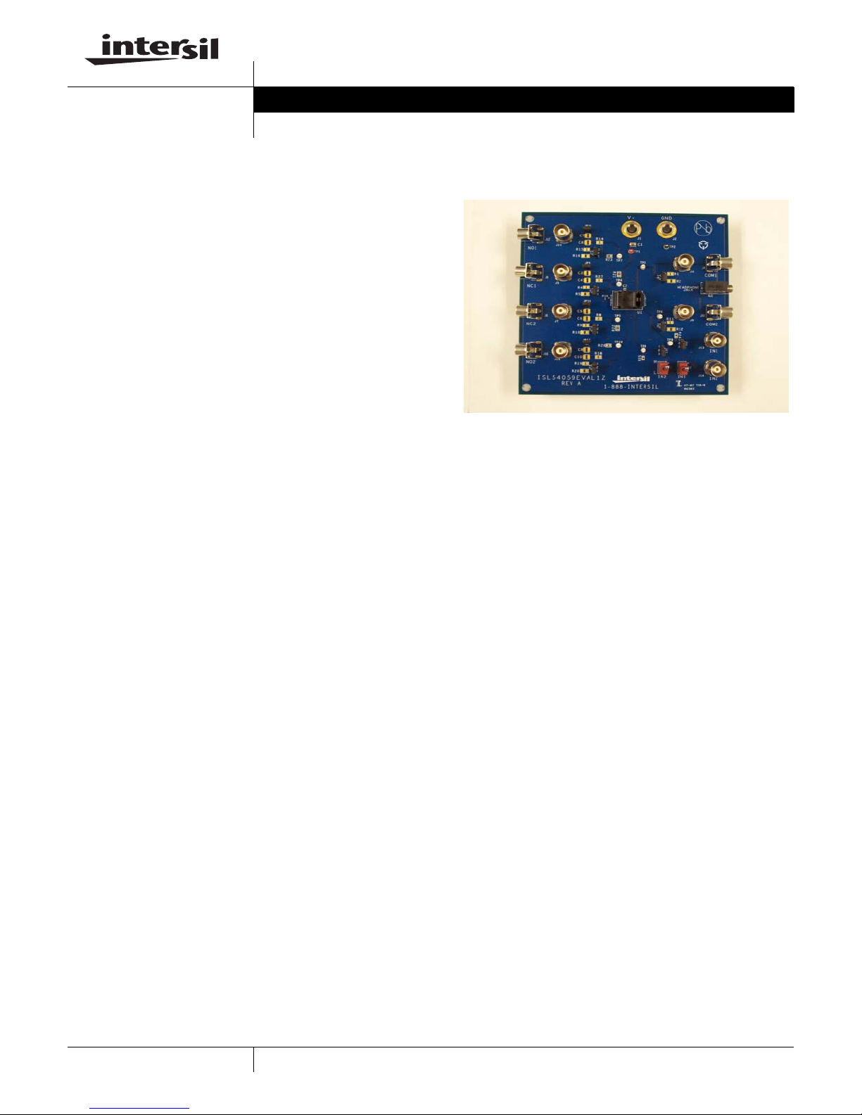
Picture of Evaluation Board (Top View)
FIGURE 1. ISL54059EVAL1Z THROUGH ISL54064EV AL1Z
EVALUATION BOARD
Board Architecture/Layout
Basic Layout of Evaluation Board
A picture of the evaluation board is located in Figure 1. The
ISL540XX IC is located inside socket U1 located at the
center of the evaluation board. The IC needs to be
orientated inside the socket such that the pin 1 indicator on
the IC is aligned with the pin 1 indicator dot inside the
socket. The evaluation board integrates the necessary
connections and components to interface with the ICs for
ease of operation.
Power Supply
The ISL540XX IC requires a supply voltage in the range of
+1.8V to +6.5V for proper operation. Banana jacks for V
(J1) and GND (J2) are located at the top of the board. The
evaluation board contains a 10µF bulk capacitor and a 0.1µF
high frequency decoupling capacitor at the supply lines.
Logic Control
The evaluation board contains two types of logic control to
the digital logic inputs of the IC available to the user. The
logic pins can be controlled either through manual or
external operation. The logic control pins are manually
toggled by the SPST switches mounted on the evaluation
board (S1-S2). When the switch is in the up position (H), the
associated logic pin is pulled to V
the switch is in the down position (L), the associated logic
pin is pulled to GND for logic LOW. For manual operation,
the jumpers JP6-JP7 need to be in the 2-3 position.
for logic HIGH. When
CC
CC
1
For external control via a function generator or switch ed
source, set the jumpers JP6-JP7 in the 1-2 position. This
by-passes the SPST switches and routes the logic control to
CAUTION: These devices are sensitive to electrostatic discharge; follow proper IC Handling Procedures.
1-888-INTERSIL or 1-888-468-3774
| Intersil (and design) is a registered trademark of Intersil Americas Inc.
All other trademarks mentioned are the property of their respective owners.
Copyright Intersil Americas Inc. 2009. All Rights Reserved
Page 2
Application Note 1369
the BNC connectors J13-J14 located on the bottom right side
of the board.
Note: There are 500k
Ω logic pull-down resistors on the INx
control pins. In external control mode when the digital logic
input lines are left in a floating state, these pull-down resistors
bias the logic inputs to ground.
Switch Terminals
The evaluation board contains components to interface with
all six terminals of the Dual SPDT switch (four terminals for
the SPST switches). The common (COM) terminals of the
switch are located on the right side of the evaluation board.
The Normally Open (NO) and Normally Closed (NC) terminals
of the switch are located on the left side of the evaluation
board. All switch terminals include both RCA jacks and BNC
connectors. The COM terminals also include a headphone
jack (HJ1) for connecting a stereo headphone or li ne level
plug.
Note: There are 10kΩ pull-down resistors on the NCx and
NOx pins of the evaluation board (R21, R22, R23, and R26).
They will need to be depopulated if the user does not desire to
have them.
Refer to Table 1 for a list of the connections on the
ISL540XXEV AL1Z and the associated pin of the IC. The
evaluation board also includes Test Points for convenient
locations to probe specific pins on the IC.
TABLE 1. BOARD COMPONENT TABLE
DEVICE
PIN
V
CC
GND J2 TP2 All
IN1 S2, J13 TP8 All
IN2 S1, J14 TP9 All
NO1 J11, J12 TP7 ISL54059,
NC1 J5, J6 TP4 ISL54059,
COM1 J3, J4, HJ1 TP3 All
NO2 J15, J16 TP10 ISL54059,
NC2 J7, J8 TP5 ISL54059,
COM2 J9, J10, HJ1 TP6 All
EVAL UA TION BOARD
CONNECTION
J1 TP1 All
TEST
POINT
APPLICABLE
IC
ISL54060,
ISL54062,
ISL54063
ISL54061,
ISL54062,
ISL54064
ISL54060,
ISL54062,
ISL54063
ISL54061,
ISL54062,
ISL54064
Note: All switch terminals on the evaluation board have
place holders that can have surface mounted components
placed either in series with the switch path or shunted to
ground. Jumpers on these components allow flexible
configurations. Refer to the Evaluation Board Schematics
located on page 4 for clarification.
Power Supply
The DC power supply connected at banana jacks J1 (VCC)
and J2 (GND) provides power to the evaluation board. The
evaluation board requires a +1.8V to +6.5V DC power
supply for proper operation. The power supply should be
capable of delivering 100µ
A of current.
Logic Control
The state of the ISL540XX IC is determined by the Truth
Table as defined in their respective datasheet. When in
manual operation mode, the logic being toggled by the
SPST switches (S1-S2) will always drive the voltage of the
logic pin to V
for a HIGH and GND for a LOW. In external
CC
control mode, the voltages being driven by an external
source must meet appropriate V
and VIL levels as defined
IH
in the datasheet.
The control pins are 1.8V logic compatible up to a +3.3V
supply, which allows for control via a standard µcontroller.
Logic “0” (LOW) when ≤ 0.5V (or floating)
Logic “1” (HIGH) when ≥1.4V
When operating above +3.3V supply, refer to the datasheet
for appropriate logic levels to drive the logic pins. It is always
recommended to drive the logic pins to the positive supply
rail (V
) and GND to minimize power consumption.
CC
Logic States
INPUT SELECT (INX) PINS
If the INx Pins are logic “HIGH”, then the NOx switches are
turned ON and the NCx switches are turned OFF. If the INx
Pins are logic “LOW”, then the NCx switches are turned ON
and the NCx switches are turned OFF.
CLICK AND POP OPERATION (ISL54062, ISL54063,
ISL54064 ONLY)
Single supply audio sources are biased at a DC offset that
generates transients during power ON/OFF of the audio
source. This DC offset is coupled through a blocking
capacitor that is need to remove the DC bias to the speaker,
causing a transient voltage at the load. For example, when
the source is OFF and suddenly turned ON with a DC offset,
the capacitor will develop a voltage equal to the DC offset.
This voltage gets discharged by the speaker causing a click
and pop noise. The ISL54062, ISL54063, and ISL54064 ICs
integrate circuitry to eliminate click and pop noises to the
speaker.
For proper operation of Click and Pop elimination, the switch
terminal that is being connected to the speaker should be
connected through the integrated shunt resistor before
2
AN1369.0
February 3, 2009
Page 3

AUDIO SOURCE
SIGNAL
LEFT
RIGHT
Application Note 1369
DC POWER
SUPPLY
+1.8V TO +6.5V
-
+
FIGURE 2. BASIC EVALUATION TEST SETUP BLOCK DIAGRAM
AUDIO SIGNAL
OSCILLOSCOPE
CHA
LOGIC CONTROL
CHB
connecting to the load. This allows any transients generated
by the source to be discharged through the shunt resistor
first, eliminating any audible click and pop noises. With a
typical DC blocking capacitor of 200µF and the shunt
resistance having a typical value of 140Ω, allowing a 250ms
dead time in for discharging a transient will eliminate the
click and pop noise.
Applications
The ISL540XX ICs are designed to be a Dual SPDT or
SPST switch for multiplexing or switching of signals that
require low insertion loss, low power consumption, and
negative voltage swing capability. Such applications include
Audio/Video equipment, battery or portable devices and
medical equipment. In addition, the Click and Pop
Elimination Circuitry makes it ideal for portable audio such
as MP3 players and cell phones.
Using The Board (Refer to Figure 2)
Lab Equipment
The equipment, external supplies and signal sources
needed to operate the board are listed below:
1. +1.8V to +6.5V DC Power Supply
2. Audio Signal Generator
3. Audio Signal Oscilloscope
4. Logic Control Generator and/or Pulse Generator
Initial Board Setup Procedure
1. Attach the evaluation board to the DC power supply at J1
) and J2 (GND). Positive terminal at J1 and negative
(V
CC
terminal at J2. The supply should be capable of delivering
+1.8V to +6.5V and 100µA of current.
2. Connect the Audio Source Signal to the NOx or NCx BNC
inputs . The analog input voltage range can be from
VCC-6.5V up to VCC.
3. Connect the Audio Signal Oscilloscope to the COMx BNC
outputs .
4. Connect the Logic Control generator to the INx logic
inputs.
NCx Switches Active
1. Drive the INx pins to logic “LOW”.
2. The NCx switches are now connected to the COMx
terminals (ISL54059, ISL54061, ISL54062, and
ISL54064 only).
3. The NOx switches have shunt resistors on the terminals
to ground (ISL54062 and ISL54063 only).
NOx Switches Active
1. Drive the INx pins to logic “HIGH”.
2. The NOx switches are now connected to the COMx
terminals (ISL54059, ISL54060, ISL54062 and ISL54063
only).
3. The NCx switches have shunt resistors on the terminals
to ground (ISL54062 and ISL54064 only).
Intersil Corporation reserves the right to make changes in circuit design, software and/or specifications at any time without notice. Accordingly, the reader is cautioned to
verify that the Application Note or Technical Brief is current before proceeding.
For information regarding Intersil Corporation and its products, see www.intersil.com
3
AN1369.0
February 3, 2009
Page 4

4
AN1369.0
February 3, 2009
ISL54059EVAL1Z Through ISL54064EVAL1Z Evaluation Board Schematic
COM1
COM1
NC2
NC1
NO1
IN2
NO2
JACK
HEADPHONE
NC2
V+
IN2
NC1
GND
NO2
IN1
NO1
COM2
COM2
IN1
IN1
IN2
R14
2
2
TP9
TP4
DNP
U1
4
1
TP5
10k
JP4
1
OPEN
2
1
J10
J1
8
R23
R24
10k
U1
9
1
499k
JP6
2
1
1
0.1µF
10µF
1
1
1
1
J2
C6
2
R25
2
21
R26
21
21
R21
21
R22
2
1
R1
21
R4
21
R9
21
R11
21
R19
21
R15
21
R16
21
R20
21
21
R12
21
R10
21
R2
21
JP10
21
JP9
21
JP12
21
JP11
5
4
3
2
1
HJ1
10
U1
U1
7
U1
6
U1
5
U1
3
U1
2
U1
1
U1
21
C4
1
21
C10
1
TP8
1
313
2
1
JP7
1
3
2
S1
5
4
3
2
1
J13
3
2
1
JP5
1
TP7
432
1
J12
21
C8
1
1
C7
5
4
3
2
1
J11
3
2
1
JP8
1
1
432
1
5
4
3
2
1
J9
3
2
1
1
TP6
4
3
2
J8
3
2
1
JP3
21
R8
5
4
3
2
1J72
C5
1
TP3
3
2
1
JP1
21
R27
2
C3
4
3
2
1
J6
5
4
3
2
1
1
TP10
TP2
TP1
1
3
2
S2
3
2
1
JP2
21
C2
21
C9
21
R18
2
C1
4
3
2
1
J4
4
3
2
1
J16
5
4
3
2
1
J15
5
43
2
1
J3
5
4
3
2
1
J14
499k
DNP
DNP
10k
DNP
DNP
DNP
DNP
DNP
DNP
DNP
DNP
DNP
OPEN
OPEN
OPEN
DNP
DNP
DNP
OPEN
OPEN
OPEN
OPEN
DNP
10k
R5
J5
V+
V+
V+
5
Application Note 1369
 Loading...