

®
ISL54000, ISL54001, ISL54002
Data Sheet June 28, 2007
Integrated Audio Amplifier Systems
The Intersil ISL54000, ISL54001, ISL54002 family of devices
are integrated audio power amplifier systems that combine
stereo BTL 8Ω amplifiers in a single package. The devices are
designed to operate from a single +2.7V to +5V power supply .
All devices are offered in a 2 0 Ld 4x4 thin QFN p ackag e.
Targeted applications include handheld equipment such as
cell-phones, MP3 players, and games/toys.
The ISL54000, ISL54001, ISL54002 parts contain two class
AB bridge-tied (BTL) type power amplifiers for driving stereo
8Ω speakers. Each BTL is capable of delivering 800mW (typ)
with 0.4% THD+N and 941mW (typ) with 1% THD+N of
continuous average power into an 8Ω BTL speaker load
when using a 5V supply.
The ISL54001 and ISL54002 feature a 2:1 stereo input
multiplexer front-end. This allows selection between two
stereo sources. In addition the ISL54002 has the capability
of mixing the stereo inputs.
All devices in this family feature low power shutdown,
thermal overload protection and click/pop suppression. The
click and pop circuitry eliminates audible transients during
audio source changes and transitioning in and out of
shutdown.
FN6458.1
Features
• Pb-Free Plus Anneal (RoHS Compliant)
• Class AB 941mW Stereo BTL Speaker Amplifiiers
• Single Supply Operation . . . . . . . . . . . . . . . . .+2.7V to +5.5V
• THD+N at 1kHz, 800mW into 8Ω . . . . . . . . . . . . . . . . . .0.4%
• THD+N at 1kHz, 941mW into 8Ω . . . . . . . . . . . . . . . . . . . 1%
• Low Power Shutdown
• Thermal Shutdown Protection
• “Click and Pop” Suppression Circuitry
• 2:1 Stereo Input Mux (ISL54001, ISL54002)
• Mixing of Two Stereo Inputs (ISL54002)
• TTL Logic-Compatible
• Available in 20 Ld 4x4 Thin QFN
Applications
• Battery powered, Handheld, and Portable Equipment
- Cellular/mobile Phones
- PDA’s, MP3 Players, DVD Players, Cameras
- Laptops, Notebooks, Palmtops
- Handheld Games and Toys
• Desktop Computers
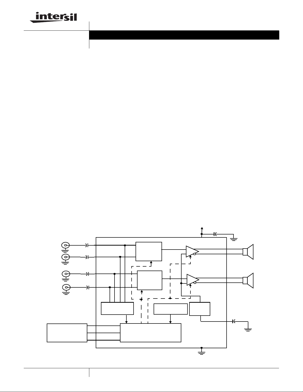
ISL54002 Typical Application Circuit and Block Diagram
RIGHT AUDIO 1
RIGHT AUDIO 2
LEFT AUDIO 1
LEFT AUDIO 2
CONTROLLER
0.22µF
0.22µF
0.22µF
0.22µF
MICRO
IN
1R
IN
2R
IN
1L
IN
2L
CLICK AND POP
SD
INS
MIX
MUX/MIXER
MUX/MIXER
THERMAL
PROTECTION
LOGIC CONTROL
BTL
BTL
V
DD
BIAS
GND
0.1µF
OUTR+
OUTR-
OUTL+
OUTL-
REF
C
1µF
REF
1
CAUTION: These devices are sensitive to electrostatic discharge; follow proper IC Handling Procedures.
1-888-INTERSIL or 1-888-468-3774
| Intersil (and design) is a registered trademark of Intersil Americas Inc.
All other trademarks mentioned are the property of their respective owners.
Copyright Intersil Americas Inc. 2007. All Rights Reserved
ISL54000, ISL54001, ISL54002
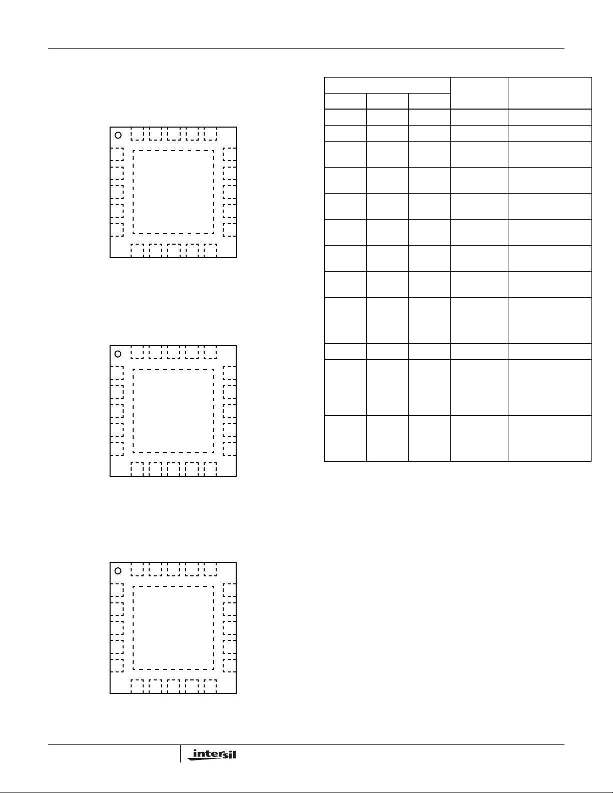
Pinouts
OUTL+
OUTR+
OUTL+
OUTR+
OUTL-
V
DD
GND
OUTL-
V
DD
GND
ISL54000
(20 LD 4X4 TQFN)
TOP VIEW
GND
20 19 18 17 16
1
2
3
4
5
678910
DD
V
NC
NC
DD
V
OUTR-
ISL54001
(20 LD 4X4 TQFN)
TOP VIEW
2R
GND
20 19 18 17 16
1
2
3
4
5
678910
INS
IN
R
IN
GND
1R
IN
N.C.
REF
N.C.
Pin Descriptions
PIN
NAME FUNCTIONISL54000 ISL54001 ISL54002
3, 6, 8, 12 3, 6, 8, 12 3, 6, 8, 12 V
DD
4, 9, 20 4, 9, 20 4, 9, 20 GND Ground Connection
N.C.
15
SD
14
NC
13
11 11 11 IN
-1313IN
17 17 17 IN
V
12
DD
IN
11
L
-1919IN
1L
2L
1R
2R
2, 5 2, 5 2, 5 OUT_+ Positive Speaker
1, 7 1, 7 1, 7 OUT_- Negative Speaker
14 14 14 SD Shutdown, High to
- 18 18 INS Input Select
NC
15
SD
14
IN
13
2L
V
12
DD
IN
11
1L
- - 16 MIX Mixer, High to mix
10 10 10 REF Common-mode Bias
System Power Supply
Left Channel Audio
Input 1
Left Channel Audio
Input 2
Right Channel Audio
Input 1
Right Channel Audio
Input 2
Output
Output
disable amplifiers,
Low for normal
operation.
Right and Left Audio
Inputs, Low to pass
Audio Inputs without
mixing
Voltage, Bypass with
a 1µF capacitor to
GND.
OUTL-
OUTL+
V
DD
GND
OUTR+
DD
V
DD
V
OUTR-
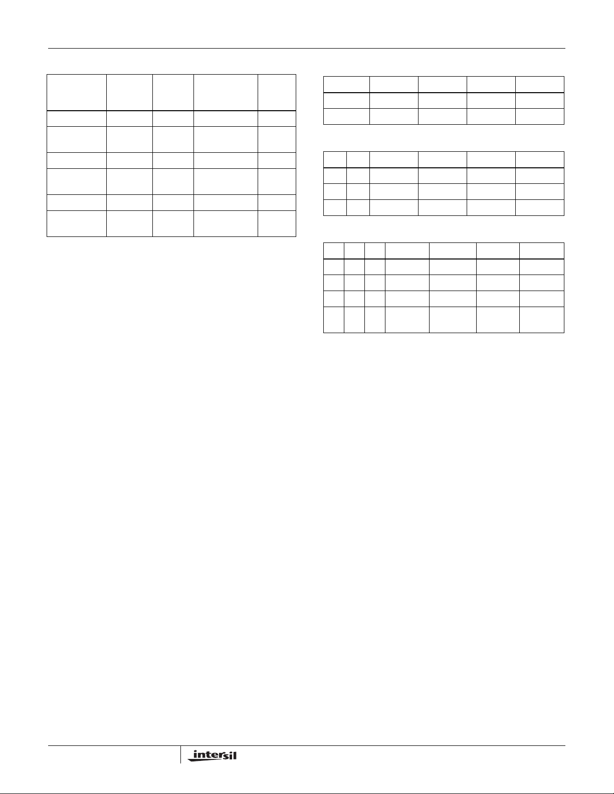
ISL54002
(20 LD 4X4 TQFN)
TOP VIEW
2R
GND
20 19 18 17 16
1
2
3
4
5
678910
DD
V
INS
IN
DD
V
OUTR-
2
GND
1R
IN
GND
REF
MIX
REF
NC
15
SD
14
IN
13
2L
V
12
DD
IN
11
1L
FN6458.1
June 28, 2007
ISL54000, ISL54001, ISL54002
Ordering Information
TEMP.
PART
NUMBER
PART
MARKING
RANGE
(°C) PACKAGE
ISL54000IR* 540 00IR -40 to +85 20 Ld 4x4 TQFN L20.4x4A
ISL54000IRTZ*
(Note)
540 00IRTZ -40 to +85 20 Ld 4x4 TQFN
(Pb-free)
ISL54001IR* 540 01IRT -40 to +85 20 Ld 4x4 TQFN L20.4x4A
ISL54001IRTZ*
(Note)
540 01IRTZ -40 to +85 20 Ld 4x4 TQFN
(Pb-free)
ISL54002IR* 540 02IRT -40 to +85 20 Ld 4x4 TQFN L20.4x4A
ISL54002IRTZ*
(Note)
540 02IRTZ -40 to +85 20 Ld 4x4 TQFN
(Pb-free)
*Add “-T” suffix for tape and reel.
NOTE: Intersil Pb-free products employ special Pb-free material sets;
molding compounds/die attach materials and 100% matte tin plate
termination finish, which are RoHS compliant and compatible with both
SnPb and Pb-free soldering operations. Intersil Pb-free products are
MSL classified at Pb-free peak reflow temperatures that meet or
exceed the Pb-free requirements of IPC/JEDEC J STD-020C.
PKG.
DWG. #
L20.4x4A
L20.4x4A
L20.4x4A
ISL54000 Truth Table
SD OUTR+ OUTR- OUTL+ OUTL-
1 Disabled Disabled Disabled Disabled
0IN
R
IN
R
IN
L
IN
ISL54001 Truth Table
SD INS OUTR+ OUTR- OUTL+ OUTL-
1 X Disabled Disabled Disabled Disabled
00 IN
01 IN
1R
2R
IN
IN
1R
2R
IN
1L
IN
2L
IN
IN
ISL54002 Truth Table
SD MIX INS OUTR+ OUTR- OUTL+ OUTL-
1 X X Disabled Disabled Disabled Disabled
000 IN
001 IN
1R
2R
01XIN1R +
IN
2R
IN
1R
IN
2R
IN1R +
IN
2R
IN
1L
IN
2L
IN1L +
IN
2L
IN
IN
IN1L +
IN
L
1L
2L
1L
2L
2L
3
FN6458.1
June 28, 2007
ISL54000, ISL54001, ISL54002
Absolute Maximum Ratings Thermal Information
VDD to GND . . . . . . . . . . . . . . . . . . . . . . . . . . . . . . . -0.3V to +6.0V
Input Voltages
In_R, In_L, SD, INS, MIX . . . . . . . . . . . . . . -0.3V to (VDD + 0.3V)
Output Voltages
OUT_+, OUT_-. . . . . . . . . . . . . . . . . . . . . . -0.3V to (VDD + 0.3V)
Continuous Current (VDD, OUT_, GND). . . . . . . . . . . . . . . . 750mA
ESD Rating
Human Body Model . . . . . . . . . . . . . . . . . . . . . . . . . . . . . . . .>2kV
Machine Model. . . . . . . . . . . . . . . . . . . . . . . . . . . . . . . . . . .>200V
Charged Device Model. . . . . . . . . . . . . . . . . . . . . . . . . . . . . .>1kV
Operating Conditions
Temperature Range. . . . . . . . . . . . . . . . . . . . . . . . . .-40°C to +85°C
CAUTION: Do not operate at or near the maximum ratings listed for extended periods of time. Exposure to such conditions may adversely impact product reliability and
result in failures not covered by warranty.
NOTE:
is measured in free air with the component mounted on a high effective thermal conductivity test board with “direct attach” features. θ
1. θ
JA
“case temp” is measured at the center of the exposed metal pad on the package underside. See Tech Brief TB379.
2. For θ
, the “case temp” location is the center of the exposed metal pad on the package underside.
JC
Thermal Resistance (Typical, Notes 1, 2) θ
(°C/W) θJC (°C/W)
JA
20 Ld 4x4 TQFN Package . . . . . . . . . . 45 6.5
Maximum Junction Temperature . . . . . . . . . . . . . . . . . . . . . . +150°C
Maximum Stor age Temperat ure Rang e. . . . . . . . . . . -65°C to +150°C
Pb-free reflow profile . . . . . . . . . . . . . . . . . . . . . . . . . .see link below
http://www.intersil.com/pbfree/Pb-FreeReflow.asp
the
JC,
Electrical Specifications - 5V Supply Test Conditions: V
C
= 1µF, RL is terminated between OUT_+ and OUT_ -, Unless Otherwise Specified
REF
= +5V, GND = 0V, V
DD
= 2.4V, V
INH
= 0.8V, SD = MIX = INS = V
INL
INL
(Note 3).
PARAMETER TEST CONDITIONS
TEMP
(°C)
MIN
(Notes 4, 5) TYP
MAX
(Notes 4, 5) UNITS
GENERAL
Power Supply Range, V
DD
Quiescent Supply Current, I
Shutdown Supply Current, I
Input Resistance, R
Thermal Shutdown, T
IN
SD
DD
SD
INS = MIX = V
coupled to ground (0.1μF)
INS = MIX = V
coupled to ground (0.1μF)
SD = V
INH
or V
INL
INH
or V
INL
INH
, INS = MIX = V
, RL = 8Ω (BTL) , Inputs A C
, RL = None, Inputs AC
or V
INL
INH
Inputs AC coupled to ground (0.1μF)
INS = 0V or V
INS = MIX = 0V or V
DD
DD
, RL = 8Ω (BTL),
Full 2.7 - 5.5 V
25 - 4.7 50 mA
Full - 10 - mA
25 - 4.6 12 mA
Full - 5.5 - mA
25 - 28 50 μA
Full - 31 - μA
25 - 100 - kΩ
25 - 150 - °C
Thermal Shutdown Hysteresis 25 - 10 - °C
SD to Full Operation, t
SD(ON)
INS = 0V or 5V, MIX = 0V or 5V Full - 1 - ms
BTL AMPLIFIER DRIVER
Output Offset Voltage, V
OS
Power Supply Rejection Ratio,
PSRR
Output Power, P
OUT
Total Harmonic Distortion + Noise,
THD + N
Max Output V oltage Swing, V
OUT
Signal to Noise Ratio, SNR RL = 8Ω, P
Measured OUT_+ and OUT_-, Input AC coupled to
ground (0.1μF)
V
RIPPLE
= 200mV
, RL = 8Ω,
P-P
Input AC coupled to ground
(0.1μF)
F
RIPPLE
F
RIPPLE
= 217Hz 25 - 49 - dB
= 1kHz 25 - 47 - dB
25 -150 45 150 mV
Full - 49 - mV
RL = 8Ω, THD + N = 1%, f = 1kHz 25 - 941 - mW
= 8Ω, THD + N = 10%, f = 1kHz 25 - 1.23 - W
R
L
R
= 8Ω, P
L
= 8Ω, P
R
L
RL = 8Ω, V
= 800mW, f = 1kHz 25 - 0.4 - %
OUT
= 800mW, f = 20Hz to 20kHz 25 - 0.7 - %
OUT
= 5V
SIGNAL
= 900mW, f = 1kHz 25 - 85 - dB
OUT
, f = 1kHz 25 7.2 7.7 - V
P-P
,
P-P
4
FN6458.1
June 28, 2007

ISL54000, ISL54001, ISL54002
Electrical Specifications - 5V Supply Test Conditions: V
C
= 1µF, RL is terminated between OUT_+ and OUT_ -, Unless Otherwise Specified
REF
(Note 3). (Continued)
PARAMETER TEST CONDITIONS
Output Noise, N
OUT
Crosstalk
R
to LCH, LCH to R
CH
CH
Off-Isolation SD = V
Channel Gain Matching
R
to L
CH
CH
Channel Phase Matching
R
to L
CH
CH
LOGIC INPUT
Input Leakage Current, I
Input Leakage Current, I
V
INH
V
INL
SD
SD
, I
INS
, I
INS
A - Weight filter, BW = 22Hz to 22kHz 25 - 125 - μV
RL = 8Ω, P
from the input of active amplifier to the output of an
= 800mW, f = 1kHz, Signal coupled
OUT
adjacent amplifier with its input AC coupled to ground.
INH, POUT
coupled from input to output of a disabled amplifier.
= 800mW, f = 10kHz, Signal
RL = 8Ω, VINxR = VINxL = 3.88V
same source)
RL = 8Ω, VINxR = VINxL= 3.88V
same source)
, I
MIXVDD
, I
MIXVDD
= 5V, SD = 0V, INS = 0V, MIX = 0V 25 -3 1.9 3 μA
= 5V, SD = VDD, INS = VDD, MIX = V
= +5V, GND = 0V, V
DD
(Connect to the
P-P
(Connect to the
P-P
DD
INH
TEMP
(°C)
= 2.4V, V
(Notes 4, 5) TYP
= 0.8V, SD = MIX = INS = V
INL
MIN
(Notes 4, 5) UNITS
INL
MAX
25 - 80 - dB
25 - 110 - dB
25 - +-0.1 - dB
25 - 0.01 - °
Full - 1.9 - μA
25 -1 0.02 -1 μA
Full - 0.02 - μA
Full 2.4 - - V
Full - - 0.8 V
,
RMS
Electrical Specifications - 3.6V Supply Test Conditions: V
GSO = GS1 = V
Unless Otherwise Specified (Note 3).
PARAMETER TEST CONDITIONS
GENERAL
Quiescent Supply Current, I
Shutdown Supply Current, I
DD
SD
BTL AMPLIFIER DRIVER, HD = V
Output Offset Voltage, V
OS
Power Supply Rejection Ratio, PSRR V
Output Power, P
OUT
Total Harmonic Distortion + Noise,
THD + N
Max Output Voltage Swing, V
OUT
INS = 0V or VDD, MIX = 0V or VDD, RL = 8Ω (BTL) ,
Input AC coupled to ground (0.1μF)
INS = 0V or V
, MIX = 0V or VDD, RL = None, Input
DD
AC coupled to ground (0.1μF)
INS = 0V or VDD, MIX = 0V or VDD, RL = 8Ω (BTL),
Input AC coupled to ground (0.1μF)
INH,
HO = V
UNLESS OTHERWISE SPECIFIED
INH,
Measured between OUT_+ and OUT_-, Input AC
coupled to ground (0.1μF)
= 200mV
RIPPLE
Input AC coupled to ground
, RL = 8Ω,
P-P
(0.1μF)
F
F
RL = 8Ω, THD + N = 1%, f = 1kHz 25 - 310 - mW
R
= 8Ω, THD + N = 10%, f = 1kHz 25 - 528 - mW
L
= 8Ω, P
R
L
= 8Ω, P
R
L
RL = 8Ω, V
= 200mW, f = 1kHz 25 - 0.4 - %
OUT
= 200mW, f = 20Hz to 20kHz 25 - 0.4 - %
OUT
SIGNAL
= 3.6V
, f = 1kHz 25 - 5.8 - V
P-P
= +3.6V, GND = 0V, V
DD
, C
INL
= 1µF. RLis terminated between OUT_+ and OUT_ -,
REF
TEMP
(°C)
= 1.4V. V
INH
INL
MIN
(Notes 4, 5) TYP
= 0.4V, SD = MIX = INS =
25 - 4 50 mA
Full - 10 - mA
25 - 2.7 12 mA
Full - 3 - mA
25 - 13 50 μA
Full - 15 - μA
25 -150 38 150 mV
Full - 58 - mV
= 217Hz 25 - 49 - dB
RIPPLE
= 1kHz 25 - 47 - dB
RIPPLE
MAX
(Notes 4, 5) UNITS
P-P
5
FN6458.1
June 28, 2007

ISL54000, ISL54001, ISL54002
Electrical Specifications - 3.6V Supply Test Conditions: V
GSO = GS1 = V
Unless Otherwise Specified (Note 3). (Continued)
PARAMETER TEST CONDITIONS
= +3.6V, GND = 0V, V
DD
, C
INL
= 1µF. RLis terminated between OUT_+ and OUT_ -,
REF
TEMP
(°C)
= 1.4V. V
INH
INL
MIN
(Notes 4, 5) TYP
= 0.4V, SD = MIX = INS =
MAX
(Notes 4, 5) UNITS
LOGIC INPUT
Input Leakage Current, I
SD
INS
, I
MIXVDD
= 5V, SD = 0V, INS = 0V, MIX = 0V 25 -3 1.9 3 μA
, I
Full - 1.9 - μA
Input Leakage Current, I
SD
, I
INS
, I
MIXVDD
= 5V, SD = VDD, INS = VDD, MIX = V
DD
25 -1 0.02 1 μA
Full - 0.02 - μA
V
INH
V
INL
Full 1.4 - - V
Full - - 0.4 V
NOTES:
= input voltage to perform proper function.
3. V
IN
4. The algebraic convention, whereby the most negative value is a minimum and the most positive a maximum, is used in this data sheet.
5. Parts are 100% tested at +25°C. Over temperature limits established by characterization and are not production tested.
ISL54000 Typical Application Circuit and Block Diagram
0.1µF
RIGHT AUDIO
LEFT AUDIO
CONTROLLER
MICRO
0.22µF
0.22µF
IN
R
IN
L
CLICK AND POP
SD
THERMAL
PROTECTION
LOGIC CONTROL
BTL
BTL
V
BIAS
GND
DD
OUTR+
OUTR-
OUTL+
OUTL-
REF
C
1µF
REF
6
FN6458.1
June 28, 2007

ISL54000, ISL54001, ISL54002
ISL54001 Typical Application Circuit and Block Diagram
0.1µF
RIGHT 1 AUDIO
RIGHT 2 AUDIO
LEFT 1 AUDIO
LEFT 2 AUDIO
CONTROLLER
0.22µF
0.22µF
0.22µF
0.22µF
MICRO
IN
1R
IN
2R
IN
1L
IN
2L
CLICK AND POP
SD
INS
MUX
MUX
THERMAL
PROTECTION
LOGIC CONTROL
BTL
BTL
ISL54002 Typical Application Circuit and Block Diagram
V
DD
BIAS
GND
OUTR+
OUTR-
OUTL+
OUTL-
REF
C
1µF
REF
RIGHT 1 AUDIO
RIGHT 2 AUDIO
LEFT 1 AUDIO
LEFT 2 AUDIO
CONTROLLER
MICRO
0.22µF
0.22µF
0.22µF
0.22µF
IN
1R
IN
2R
IN
1L
IN
2L
CLICK AND POP
SD
INS
MIX
MUX/MIXER
MUX/MIXER
THERMAL
PROTECTION
LOGIC CONTROL
BLT
BLT
V
DD
BIAS
GND
0.1µF
OUTR+
OUTR-
OUTL+
OUTL-
REF
C
1µF
REF
7
FN6458.1
June 28, 2007

ISL54000, ISL54001, ISL54002
Detailed Description
The Intersil ISL54000, ISL54001, ISL54002 family of devices
are integrated audio power amplifier systems designed to
drive 8
Ω speaker loads. They can operate with a supply
voltage of +2.7V to +5V and provide good quality audio, while
requiring minimal external components. Its low 0.4% THD+N
while driving 800mW into an 8
distortion amplification of the audio signals. The devices are
offered in a 20 Ld 4x4 TQFN package. Targeted applications
include handheld equipment such as cell-phones, MP3
players, and games/toys.
The ISL54000, ISL54001, ISL54002 parts contain two class
AB bridge-tied (BTL) type power amplifiers for driving stereo
8Ω speakers. When powered with a 5V supply, each BTL is
capable of delivering 941mW (typ) of continuous average
power to an 8Ω speaker load with 1% THD+N performance.
When the speaker load is connected across the positive and
negative terminals of the BTL driver, the voltage is doubled
across the load and the power is quadrupled.
The ISL54001 and ISL54002 feature a 2:1 stereo input
multiplexer front-end. This allows selection between two
stereo sources. The INS control pin determines which stereo
input is active. Applying a logic “0” to the INS control pin
selects stereo input 1 (R1 and L1). Applying a logic “1” to the
INS control pin selects stereo input 2 (R2 and L2).
The ISL54002 has the capability of mixing the two stereo
inputs. When in MIX Mode (MIX = “1”) the ISL54002 mixes
the R1 input with the R2 input and sends the combined
signal to the OUTR_ BTL driver and it mixes the L1 input
with the L2 input and sends the combined signal to the
OUTL_ BTL driver.
All devices in this family feature low power shutdown,
thermal overload protection and click/pop suppression. The
click and pop circuitry prohibits switching between input
channels until the audio input signals are at their lowest
point, which eliminates audible transients in the speakers
when changing audio input sources. The click/pop circuitry
also keeps speaker transients to an inaudibile level when
entering and leaving shutdown.
Typical application circuits and block diagrams for each
device in the family are on page 6 and page 7.
Ω speaker ensures clean, low
required to calculate the capacitor value is:
C 1 6.28 f 100kΩ••⁄≥
The 100k
ISL54000, ISL54001, and ISL54002 devices.
Ω is the impedance looking into the input of the
(EQ. 1)
BTL Speaker Amplifiers
The ISL54000, ISL54001, and ISL54002 contains two
bridge-tied load (BTL) amplifiers designed to drive a speaker
load differentially. The output from one BTL is OUTL+ and
OUTL-. The output of the other BTL is OUTR+ and OUTR-.
A single BTL driver consists of inverting and non-inverting
power op amps. The AC signal out of each op amp are equal
in magnitude but 180° out of phase,so the AC signal at
OUTL+ and OUTL- have the same amplitude but are 180°
out of phase. The same is true of OUTR+ and OUTR-. The
speaker load gets connected between the + terminal and terminal outputs.
Driving the load differentially using a BTL configuration
doubles the output voltage across the speaker load and
quadruples the power to the load. In effect you get a gain of
two due to this configuration at the load as compared to
driving the load with a single-ended amplifier with its load
connected between a single amplifier ’s output and ground.
The outputs of each BTL are biased at V
load gets connected across the + and - terminal of the BTL,
the mid supply DC bias voltage at each output gets
cancelled out eliminating the need for large bulky output
coupling capacitors.
/2. When the
DD
Low Power Shutdown
With a logic “1” at the SD control pin the device enters the
low power shutdown state. When in shutdown the output
amplifiers go into an high impedance state and supply
current is reduced to 26
In shutdown mode before the amplifiers enter the high
impedance/low current drive state, the bias voltage of V
remains connected at the output through a 100kΩ resistor.
This resistor is not present during active operation of the
drivers but gets switched in when the SD pin goes high and
disconnected when the SD pin goes low.
μA (typ).
DD
/2
DC Bias Voltage
The ISL54000, ISL54001, and ISL54002 have internal DC
bias circuitry, which DC offsets the incoming audio signal at
V
/2. When using a 5V supply, the DC offset will be 2.5V.
DD
When using a 3.6V supply, the DC offset will be 1.8V.
Since the signal gets biased internally at V
signals need to be AC coupled to the inputs of the device.
The value of the AC coupling capacitor depends on the low
frequency range required for the application. A capacitor of
0.22
μF will pass a signal as low as 7.2Hz. The formula
8
/2, the audio
DD
Leaving the DC bias voltage connected through this 100kΩ
resistor reduces the transient that is generated across the
speaker, while going into or out of shutdown, to a level that
does not produce clicking or popping in the speaker.
QFN Thermal Pad Considerations
The QFN package features an exposed thermal pad on its
underside. This pad lowers the package’s thermal resistance
by providing a direct heat conduction path from the die to the
PCB. Connect the exposed thermal pad to GND by using a
large copper pad and multiple vias to the GND plane. The
FN6458.1
June 28, 2007

ISL54000, ISL54001, ISL54002
vias should be plugged and tented with plating and solder
mask to ensure good thermal conductivity.
Best thermal performance is achieved with the largest
practical copper ground plane area.
PCB Layout Considersations and Power
Supply Bypassing
To maintain the highest load dissipation and widest output
voltage swing the power supply PCB traces and the traces
that connect the output of the drivers to the speaker loads
should be made as wide as possible to minimize losses due
to parasitic trace resistance.
Typical Performance Curves T
1.0
0.9
VDD = 5V
0.8
BTL
= 8Ω
R
0.7
L
P
= 800mW
O
0.6
0.5
0.4
0.3
THD+N (%)
0.2
= +25°C, Unless Otherwise Specified.
A
Proper supply bypassing is necessary for high power supply
rejection and low noise performance. A filter network
consisting of a 10µF capacitor in parallel with a 0.1µF
capacitor is recommended at the voltage regulator that is
providing the power to the ISL54000, ISL54001, and
ISL54002 IC.
Local bypass capacitors of 0.1µF should be put at each V
DD
pin of the ISL54000, ISL54001, ISL54002 devices. They
should be located as close as possible to the pin, keeping
the length of leads and traces as short as possible.
A 1µF capacitor from the REF pin (pin 10) to ground is
needed for optimum PSRR and internal bias voltage stability.
1.0
VDD = 3.6V
0.9
0.8
BTL
R
0.7
= 8Ω
L
P
= 200mW
0.6
O
0.5
0.4
0.3
THD+N (%)
0.2
0.1
20 20k50 100 200 500 1k 2k 5k 10k
FREQUENCY (Hz)
FIGURE 1. THD+N vs FREQUENCY
10
VDD = 5V
5
BTL
= 8Ω
R
L
2
f = 1kHz
1
0.50
0.20
THD+N (%)
0.10
0.05
0.02
0.01
10m 120m 50m 100m 200m 500m
OUTPUT POWER (W)
FIGURE 3. THD+N vs OUTPUT POWER FIGURE 4. THD+N vs OUTPUT POWER
0.1
20 20k50 100 200 500 1k 2k 5k 10k
FREQUENCY (Hz)
FIGURE 2. THD+N vs FREQUENCY
10
VDD = 3.6V
5
BTL
= 8Ω
R
L
f = 1kHz
2
1
0.50
0.20
THD+N (%)
0.10
0.05
0.02
0.01
10m 600m20m 40m 70m 100m 200m
OUTPUT POWER (W)
9
FN6458.1
June 28, 2007

ISL54000, ISL54001, ISL54002
Typical Performance Curves T
-40
VDD = 5V
-45
= 800mW
P
O
-50
-55
-60
-65
-70
-75
-80
-85
-90
CROSSTALK (dB)
-95
-100
-105
-110
-115
-120
20 20k50 100 200 500 1k 2k 5k 10k
FIGURE 5. CROSSTALK vs FREQUENCY FIGURE 6. OFFISOLATION vs FREQUENCY
-20
-22
VDD = 5V
-24
BTL
-26
-28
-30
-32
-34
-36
-38
-40
-42
-44
-46
-48
-50
PSRR (dB)
-52
-54
-56
-58
-60
-62
-64
-66
-68
-70
10 20k20 50 100 200 500 1k 2k 5k 10k
V
RIPPLE
= 200mV
P-P
FIGURE 7. PSRR vs FREQUENCY
RCH TO L
LCH TO R
FREQUENCY (Hz)
FREQUENCY (Hz)
CH
= +25°C, Unless Otherwise Specified. (Continued)
A
-80
VDD = 5V
-82
P
= 800mW
-84
O
-86
-88
-90
-92
-94
-96
-98
-100
-102
CH
-104
-106
-108
OFFISOLATION (dB)
-110
-112
-114
-116
-118
-120
20 20k50 100 200 500 1k 2k 5k 10k
700
VDD = 5V
BTL
600
R
= 8Ω
L
500
400
300
200
POWER DISSIPATION (mW)
100
0
0 250 500 750 1000
FIGURE 8. POWER DISSIPATION vs OUTPUT POWER
FREQUENCY (Hz)
P
(mW)
OUT
400
VDD = 3.6V
BTL
350
R
= 8
Ω
L
300
250
200
150
100
POWER DISSIPATION (mW)
50
0
0 100 200 300 400 500
P
OUT
(mW)
FIGURE 9. POWER DISSIPATION vs OUTPUT POWER
10
Die Characteristics
SUBSTRATE POTENTIAL (POWERED UP):
GND
PROCESS:
Submicron CMOS
FN6458.1
June 28, 2007

ISL54000, ISL54001, ISL54002
Thin Quad Flat No-Lead Plastic Package
(TQFN)
Thin Micro Lead FramePlastic Package
(TMLFP)
L20.4x4A
20 LEAD QUAD FLAT NO-LEAD PLASTIC PACKAGE
(COMPLIANT TO JEDEC MO-220WGGD-1 ISSUE I)
MILLIMETERS
SYMBOL
A 0.70 0.75 0.80 -
A1 - 0.02 0.05 -
A2 - 0.55 0.80 9
A3 0.20 REF 9
b 0.18 0.25 0.30 5, 8
D 4.00 BSC -
D1 3.75 BSC 9
D2 1.95 2.10 2.25 7, 8
E 4.00 BSC -
E1 3.75 BSC 9
E2 1.95 2.10 2.25 7, 8
e 0.50 BSC -
k0.20 - - -
L 0.35 0.60 0.75 8
N202
Nd 5 3
Ne 5 3
P- -0.609
θ --129
NOTES:
1. Dimensioning and tolerancing conform to ASME Y14.5-1994.
2. N is the number of terminals.
3. Nd and Ne refer to the number of terminals on each D and E.
4. All dimensions are in millimeters. Angles are in degrees.
5. Dimension b applies to the metallized terminal and is measured
between 0.15mm and 0.30mm from the terminal tip.
6. The configuration of the pin #1 identifier is optional, but must be
located within the zone indicated. The pin #1 identifier may be
either a mold or mark feature.
7. Dimensions D2 and E2 are for the exposed pads which provide
improved electrical and thermal performance.
8. Nominal dimensions are provided to assist with PCB Land Pattern
Design efforts, see Intersil Technical Brief TB389.
9. Features and dimensions A2, A3, D1, E1, P & θ are present when
Anvil singulation method is used and not present for saw
singulation.
NOTESMIN NOMINAL MAX
Rev. 0 11/04
All Intersil U.S. products are manufactured, assembled and tested utilizing ISO9000 quality systems.
Intersil Corporation’s quality certifications can be viewed at www.intersil.com/design/quality
Intersil products are sold by description only. Intersil Corporation reserves the right to make changes in circuit design, software and/or specifications at any time without
notice. Accordingly, the reader is cautioned to verify that data sheets are current before placing orders. Information furnished by Intersil is believed to be accurate and
reliable. However, no responsibility is assumed by Intersil or its subsidiaries for its use; nor for any infringements of patents or other rights of third parties which may result
from its use. No license is granted by implicat ion or oth erwise u nde r any p a tent or p at ent r ights of Intersil or its subsidiaries.
For information regarding Intersil Corporation and its products, see www.intersil.com
11
FN6458.1
June 28, 2007
 Loading...