

®
www.BDTIC.com/Intersil
ISL5314
Data Sheet July 28, 2005
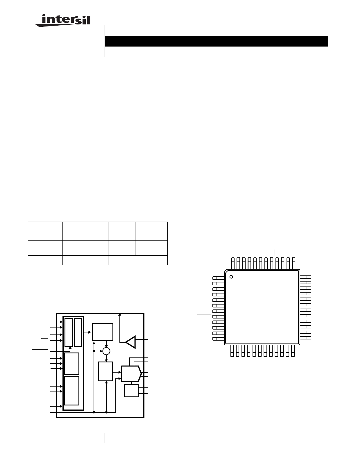
Direct Digital Synthesizer
The 14-bit ISL5314 provides a complete Direct Digital
Synthesizer (DDS) system in a single 48-pin LQFP package.
A 48-bit Programmable Carrier NCO (numerically controlled
oscillator) and a high speed 14-bit DAC (digital to analog
converter) are integrated into a stand alone DDS.
The DDS accepts 48-bit center and offset frequency control
information via a parallel processor interface. A 40-bit
frequency tuning word can also be loaded via an asynchronous
serial interface. Modulation control is provided by 3 external
pins. The PH0 and PH1 pins select phase offsets of 0, 90,
180 and 270 degrees, while the ENOFR pin enables or zeros
the offset frequency word to the phase accumulator.
The parallel processor interface has an 8-bit write-only data
input C(7:0), a 4-bit address A(3:0) bus, a Write Strobe
(WR), and a Write Enable (WE
). The processor can update
all registers simultaneously by loading a set of master
registers, then transfer all master registers to the slave
registers by asserting the UPDATE
pin.
Ordering Information
PART # TEMP. RANGE (°C) PACKAGE PKG. DW G . #
ISL5314IN -40 to 85 48 LQFP Q48.7x7A
ISL5314INZ
(See Note)
-40 to 85 48 LQFP
(Pb-free)
Q48.7x7A
ISL5314EVAL2 25 Evaluation Board
NOTE: Intersil Pb-free plus anneal products employ special Pb-free material
sets; molding compounds/die attach materials and 100% matte tin plate
termination finish, which are RoHS compliant and compatible with both SnPb
and Pb-free soldering operations. Intersil Pb-free products are MSL classified
at Pb-free peak reflow temperatures that meet or exceed the Pb-free
requirements of IPC/JEDEC J STD-020.
Block Diagram
C(7:0)
A(3:0)
WR
WE
UPDATE
SDATA
SSYNC
SCLK
ENOFR
PH(1:0)
MASTER
SLAVE
CONTROL
SERIAL
MODULATION
CONTROL
PHASE
ACCUM.
∑
SINE
WAVE
ROM
COMPOUT
+
14 BIT
DAC
INT
REF
ININ+
COMP1
COMP2
IOUTA
IOUTB
REFIO
REFLO
FN4901.2
Features
• 125MSPS output sample rate with 5V digital supply
• 100MSPS output sample rate with 3.3V digital supply
• 14-bit digital-to-analog (DAC) with internal reference
• Parallel control interface for fast tuning (50MSPS control
register write rate) and serial control interface
• 48-bit programmable frequency control
• Offset frequency register and enable pin for fast FSK
• Small 48-pin LQFP packaging
• Pb-Free plus anneal available (RoHS compliant)
Applications
• Programmable local oscillator
• FSK, PSK modulation
• Direct digital synthesis
• Clock generation
Pinout
48-PIN LQFP (Q48.7X7A)
TOP VIEW
WR
DGND
AVDD
COMP2
WE
AGND
NC
IN+
A0
IN-
A1
373839404142434445464748
36
35
34
33
32
31
30
29
28
27
26
25
2423222120191817
AGND
A2
A3
PH0
PH1
SSYNC
DVDD
SCLK
DGND
DGND
SDATA
DVDD
DGND
C2
C1
C0
ENOFR
DGND
CLK
DVDD
RESET
UPDATE
COMPOUT
REFLO
REFIO
C3
C4
1
2
3
4
5
6
7
8
9
10
11
12
13 14 15 16
FSADJ
COMP1
C6
C7
DVDD
C5
ISL5314
AGND
AGND
IOUTA
IOUTB
RESET
CLK
1
CAUTION: These devices are sensitive to electrostatic discharge; follow proper IC Handling Procedures.
1-888-INTERSIL or 1-888-468-3774
| Intersil (and design) is a registered trademark of Intersil Americas Inc.
All other trademarks mentioned are the property of their respective owners.
Copyright Intersil Americas Inc. 2000, 2005. All Rights Reserved
ISL5314
www.BDTIC.com/Intersil
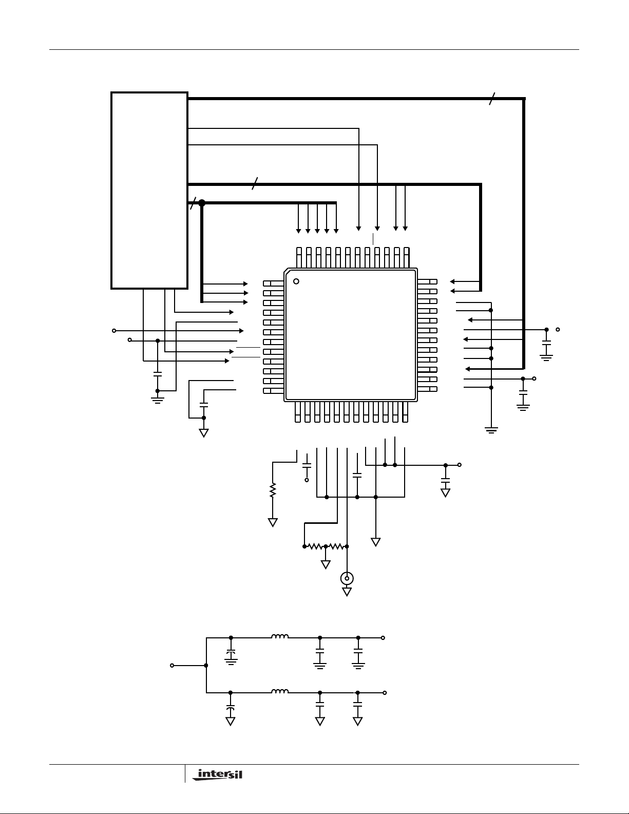
Typical Application Circuit (Parallel Control Mode, Sinewave Generation)
CLOCK
SOURCE
f
CLK
µPROCESSOR/
FPGA/CPLD
DV
PP
0.1µF
SDATA, SSYNC, SCLK (IN PARALLEL CONTROL MODE,
SERIAL CONTROL CAN ALSO BE USED IF DESIRED.)
WRITE CLOCK (WR)
WRITE ENABLE
C2
C1
C0
ENOFR
DGND
CLK
DVDD
RESET
UPDATE
REFLO
REFIO
4
C3
C6
C7
C5
DVDD
ISL5314
WR
1
2
3
4
5
6
7
8
9
10
11
12
13 14 15 16
C4
A3:A0 BUS
8
C7:C0 BUS
0.1µF
COMPOUT
DGND
WE
NC
A0
3
A1
373839404142434445464748
36
35
34
33
32
31
30
29
28
27
26
25
2423222120191817
A2
A3
PH0
PH1
SSYNC
DVDD
SCLK
DGND
DGND
SDATA
DVDD
DGND
DV
0.1µF
PP
DV
PP
0.1µF
+5V POWER SOURCE
+
+
10µF
10µF
R
SET
2kΩ
0.1µF
FERRITE
BEAD
10µH
FERRITE
BEAD
10µH
AV
FSADJ
PP
AGND
COMP1
50Ω
0.1µF
0.1µF
AGND
50Ω
DGND
AGND
AVDD
AGND
IOUTA
IOUTB
COMP2
0.1µF
(IOUTA) ANALOG OUTPUT
1µF
1µF
IN-
IN+
AGND
0.1µF
(DIGITAL POWER PLANE)
DVPP
AVPP
(ANALOG POWER PLANE)
AV
PP
2

ISL5314
www.BDTIC.com/Intersil
Functional Description
The ISL5314 is an NCO with an integrated 14-bit DAC
designed to run in excess of 125MSPS. The NCO is a 16-bit
output design, which is rounded to fourteen bits for input to the
DAC. The frequency control is the sum of a 48-bit center
frequency word, a 48-bit offset frequency word, and a 40-bit
serially loaded tuning word. The three components are added
modulo 48 bits with the alignment shown in T able 1. Each of the
three terms can be zeroed independently (via the
microprocessor interface for the center and serial frequency
registers and via the ENOFR pin for the offset frequency term).
Frequency Generation
The output frequency of the part is determined by the
summation of three registers:
f
= f
OUT
where CF is the center frequency register, OF is the offset
frequency register, SF is the serial frequency register and
f
CLK
With a 125MSPS clock rate, the center frequency can be
programmed to
(125 x 10
The addition of the frequency control words can be interpreted
as two’s complement if conv enient. F or example, if the center
frequency is set to 4000...00h and the offset frequency set to
C000..00h, the programmed center frequency would be f
and the programmed offset frequency -f
be 10000..00h, but because only the lower 48 bits are retained,
the effective frequency would be 0. In reality, frequencies above
8000...00h alias below f
the MSB is only provided as a convenience for two’s
complement calculations.
The frequency control of the NCO is the change in phase per
clock period or dφ/dt. This is integrated by the phase
accumulator to obtain frequency . The most significant 24 bits
of phase are then mapped to 16 bits of amplitude in a sine
look-up table function. The range of dφ/dt is 0–1 with 1
equaling 360 degrees or (2 x pi) per clock period. The phase
accumulator output is also 0–1 with 1 equaling 360 degrees.
The operations are modulo 48 bits because the MSB (bit 47)
aligns with the most significant address bit of the sine ROM
and the ROM contains one cycle of a sinusoid. The MSB is
weighted at 180 degrees. Full scale is 360 degrees minus
one LSB and the phase then rolls over to 0 degrees for the
next cycle of the sinusoid.
The DDS can be clocked with either a sinusoidal or a square
wave. Refer to the digital inputs V
electrical specifications table.
x ((CF + OF +SF) mod (248))/ (248),
CLK
is the DDS clock rate.
6
)/(248) = 0.4 µHz resolution.
/2 (the output of the part is real), so
CLK
/4. The sum would
CLK
and VIL values in the
IH
CLK
/4
four address pins (A3:A0), a write strobe (WR), and a write
enable (WE
processor interface loads a set of master registers. The
contents of the master set of registers is then transferred to a
slave set of registers by asserting a pin (UPDATE
allows all of the bits of the frequency control to be updated
simultaneously.
The rate which the user writes (WR) to these registers does not
have to be the same rate as the DDS clock rate (the rate of the
NCO and DAC; pin CLK). It is e x pected that most applications
will have a slower register write rate than the DDS clock rate. It
takes one WR cycle at the write rate for each register that is
written and another eleven CLK cycles at the DDS r ate to write
and obtain a new output, assuming that the UPDATE
always active . If the UPD ATE
word has been written, it takes fourteen CLK cycles, rather than
eleven. F or cases which require the output to be updated with
all of the new frequency information present, it is necessary that
the UPDATE
has been written to the device. See the Timing Diagrams for
more information. The parallel registers can be written at a rate
of CLK/2, such that updated control words can be pipelined. If
the application does not require all registers to be written, then
the output frequency can be changed more quickly . For
example, if only 32 bits of frequency information are needed
and it is desired that the output be updated all at once, then it
takes four WR cycles, then the ass ertion low of the UPD ATE
pin, plus another fourteen CLK cycles at the DDS rate to write
and update a new frequency.
The timing is the same whether writing to the center or offset
frequency registers. For f aster frequ ency update, consider the
ENOFR (Enable Offset Fr equency Register) option. Once the
values have been written to the center and offset frequency
registers, the user can enable and disab le the offset frequency
register, which is added to the center frequency value when
enabled. The ENOFR pin has a latency of fourteen CLK
cycles, but simplifies the interface because the only pin that
has to be toggled is the ENOFR pin. See the FSK explanation
for more information.
). The interface is a master/slave type. The
). This
pin is
pin is not active until after the new
be inactive until after all of the new frequency word
Serial Interface
A serial interface is provided for loading a tuning frequency .
This interface can be asynchronous to the master clock of the
part. When the tuning word has been shifted into the part, it is
loaded into a holding register by the serial interface clock,
SCLK. This loading triggers a synchronization circuit to transfer
the data to a slave register synchronous with the master clock.
A minimum of eleven serial clocks (at minimum serial word size
of eight) are necessary to complete the transfer to the slave
register. Another twelv e DDS CLK cycles are necessary before
the output of the DDS reflects the new frequency .
Parallel Interface
The processor interface is an 8-bit parallel write only
interface. The interface consists of eight data bits (C7:C0),
3
Serial loading latency = ((8 x N + 3) x SCLK)+ 12 x f
CLK
,
ISL5314
www.BDTIC.com/Intersil
TABLE 1. FREQUENCY CONTROL BIT ALIGNMENTS
48 Bits
(Individual Bit Alignment)
Phase Accumulator xxxx xxxx xxxx xxxx xxxx xxxx xxxx xxxx xxxx xxxx xxxx xxxx
Center Frequency xxxx xxxx xxxx xxxx xxxx xxxx xxxx xxxx xxxx xxxx xxxx xxxx
Offset Frequency xxxx xxxx xxxx xxxx xxxx xxxx xxxx xxxx xxxx xxxx xxxx xxxx
Serial Frequency, 8 Bits xxxx xxxx 0000 0000 0000 0000 0000 0000 0000 0000 0000 0000
Serial Frequency, 16 Bits xxxx xxxx xxxx xxxx 0000 0000 0000 0000 0000 0000 0000 0000
Serial Frequency, 24 Bits xxxx xxxx xxxx xxxx xxxx xxxx 0000 0000 0000 0000 0000 0000
Serial Frequency, 32 Bits xxxx xxxx xxxx xxxx xxxx xxxx xxxx xxxx 0000 0000 0000 0000
Serial Frequency, 40 Bits xxxx xxxx xxxx xxxx xxxx xxxx xxxx xxxx xxxx xxxx 0000 0000
4444 4444 3333 3333 3322 2222 2222 1111 1111 1100 0000 0000
7654 3210 9876 5432 1098 7654 3210 9876 5432 1098 7654 3210
where N = 1–5 (for 8–40 bit serial data) and f
clock rate. Three e xtr a SCLKs are required (one f or the SYNC
pulse plus two additional for register transfer). The latency in
seconds depends on how many bits of serial data are being
written and the speeds of both clocks. The center and offset
frequency registers cannot be written using the serial pins.
They must be programmed using the parallel interface.
In order to use the three wire serial interface in a mode that is
not the default mode, the parallel control bus must be used to
reprogram register 12. Register 12 can be set according to the
desired options of the serial interface that are described in the
register description table. Since the serial register defaults
enabled, it must be disabled in register 13 (bit 6) if it is not used.
is the DDS
CLK
Register 14
The parallel control bus must be used to program register 14
with 0x00h or 0x30h after assertion of RESET
Register table in the back of the datasheet for more information.
. See the Control
Control Pins
There are three control pins provided for phase and frequency
control. The PH0 and PH1 pins select phase offsets of 0, 90,
180, and 270 degrees and can be used for low speed,
unfiltered BPSK or QPSK modulation. These pins can also be
used for providing sine/cosine when using two ISL5314s
together as quadrature local oscillators. The ENOFR pin
enables or zeros the offset frequency word to the phase
accumulator and can be used for FSK or MSK modulation.
These control pins and the UPDATE
special cells to minimize the probability of metastability . Writing
anything to register 15 behaves like an UPDA TE
user can save one control pin if desired.
pin are passed through
so that the
Reset
A RESET pin is available which resets all registers to their
defaults. Register 14 must always be written with 0x00h or
0x30h after a RESET
take the RESET
and then take the RESET
the RESET
is eleven CLK cycles. See the register description table in
the back of the data sheet for the default states of all bits in
pin going high until the output reflects the reset
. In order to reset the part, the user must
pin low, allow at least one CLK rising edge,
pin high again. The latency from
all registers. After RESET
is required before the control registers can be written to
again. The center frequency register resets to f
offset frequency register resets to an unknown frequency but
is disabled. The serial frequency register resets to an
unknown frequency and is enabled. If the serial register is
not used, disable it in register 13 using the parallel interface.
goes high, one rising edge of CLK
/4. The
CLK
Comparator
A comparator is provided for square wave output generation.
The user can take the DDS analog output, filter it, and then
send it back into the comparator. A square wa ve will be
generated at the comparator output (COMPOUT pin) at an
amplitude level that is dependent on the digital power supply
(DV
). The comparator was designed to operate at speeds
DD
comparable to the DDS output frequency range (approximately
0–50MHz). It is not intended for low jitter applications (<0.5ns).
The comparator has a sleep mode that is activated by
connecting both inputs (IN- and IN+) to the analog power
supply plane. This will save appro ximately 4mA of current (as
shown in the Typical Application Circuit). If the comparator is
not used, leave the COMPOUT pin floating.
DAC Voltage Reference
The internal voltage reference for the DAC has a nominal
value of +1.2V with a ±60ppm/
full temperature range of the converter. It is recommended
that a 0.1µF capacitor be placed as close as possible to the
REFIO pin, connected to the analog ground. The REFLO pin
(11) selects the reference. The internal reference can be
selected if pin 11 is tied low (ground). If an external reference
is desired, then pin 11 should be tied high (the analog supply
voltage) and the external reference driven into REFIO, pin
12. The full-scale output current of the converter is a function
of the voltage reference used and the value of R
should be within the 2mA–20mA range, though operation
below 2mA is possible, with performance degradation.
If the internal reference is used, V
approximately 1.2V (pin 13). If an external reference is used,
V
I
will equal the external reference.
FSADJ
(Full Scale) = (V
OUT
FSADJ/RSET)
o
C drift coefficient over the
. I
SET
will equal
FSADJ
X 32.
OUT
4
ISL5314
www.BDTIC.com/Intersil
Analog Output
IOUT A and IOUTB are complementary current outputs. They
are generated by a 14-bit DA C that is capab le of running at the
full 125MSPS rate. The DDS clock also clocks the D A C. The
sum of the two output currents is always equal to the full scale
output current minus one LSB. If single-ended use is desired, a
load resistor can be used to convert the output current to a
voltage. It is recommended that the unused output be equally
terminated. The voltage developed at the output must not
violate the output voltage compliance range of -1.0V to +1.25V.
R
(the impedance loading each current output) should be
LOAD
chosen so that the desired output voltage is produced in
conjunction with the output full scale current. If a known line
impedance is to be driven, then the output load resistor should
be chosen to match this impedance. The output voltage
equation is:
V
= I
OUT
X R
OUT
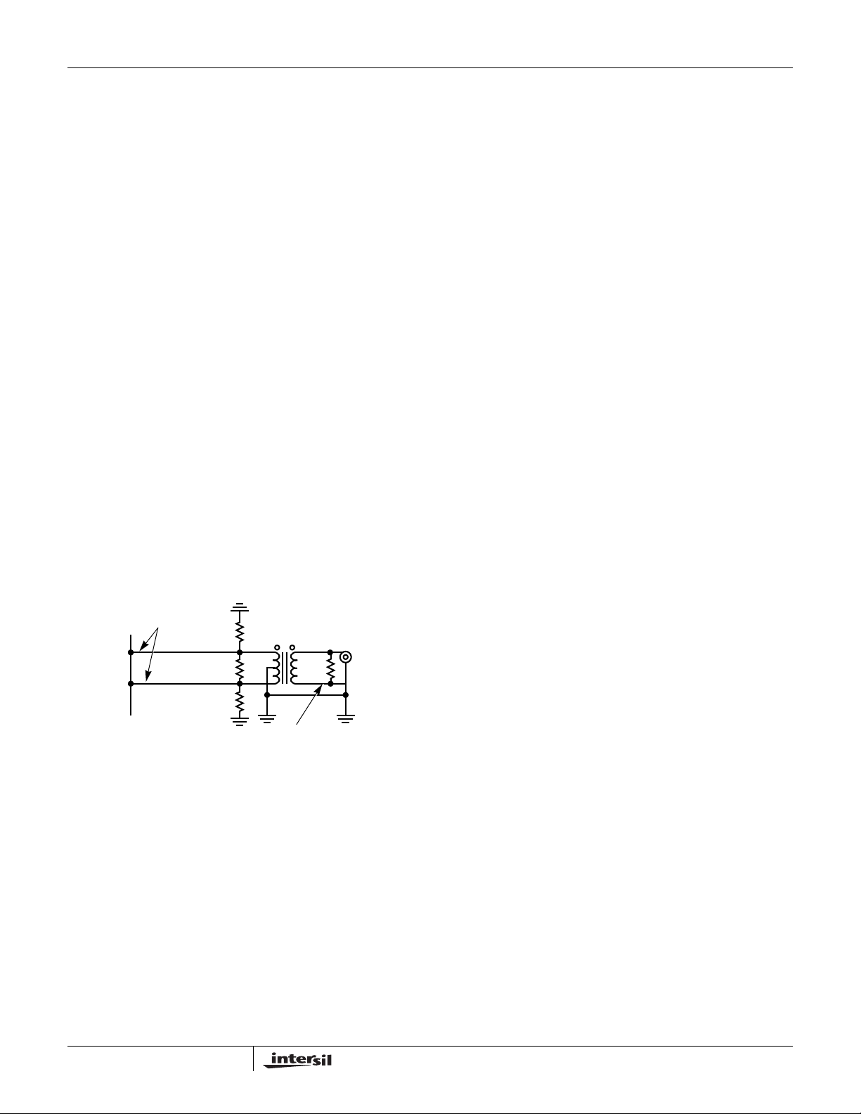
These outputs can be used in a differential-to-single-ended
arrangement. This is typically done to achieve better harmonic
rejection. Because of a mismatch in IOUT A and IOUTB , the
transformer does not improve the harmonic rejection. Howev er ,
it can provide voltage gain without adding distortion. The SFDR
measurements in this data sheet were performed with a 1:1
transformer on the output of the DDS (see Figure 1). With the
center tap grounded, the output swing of pins 17 and 18 will be
biased at zero volts. The loading as shown in Figure 1 will result
in a 500mV
signal at the output of the transformer if the full
P-P
scale output current of the DAC is set to 20mA.
REQ IS THE IMPEDANCE
LOADING EACH OUTPUT
PIN 17
PIN 18
ISL5314
FIGURE 1. TRANSFORMER OUTPUT CIRCUIT OPTION
V
= 2 x I
OUT
OUT
center tap to float will result in identical transformer output,
howeve r the output pins of the DAC will have positive DC
offset, which could limit the voltage swing available due to
the output voltage compliance range. The 50Ω load on the
output of the transformer represents the load at the end of a
‘transmission line’, typically a spectrum analyzer,
oscilloscope, or the next function in the signal chain. The
necessity to have a 50Ω impedance looking back into the
transformer is negated if the DDS is only driving a short
trace. The output voltage compliance range does limit the
impedance that is loading the DDS output.
.
LOAD
IOUTB
IOUTA
50Ω
100Ω
50Ω
= (2 x I
V
OUT
50Ω REPRESENTS THE
SPECTRUM ANALYZER
50Ω
OUT
x REQ)V
x REQ, where REQ is 12.5Ω. Allowing the
PP
Application Considerations
Ground Plane
Separate digital and analog ground planes should be used. All
of the digital functions of the device and their corresponding
components should be located over the digital ground plane
and terminated to the digital ground plane. The same is true for
the analog components and the analog ground plane. Pins 11
through 24 are analog pins, while all the others are digital.
Noise Reduction
To minimize power supply noise, 0.1µF capacitors should be
placed as close as possible to the power supply pins, AV
and DV
. Also, the layout should be designed using
DD
separate digital and analog ground planes and these
capacitors should be terminated to the digital ground for
DV
and to the analog ground for A VDD. Additional filtering
DD
of the power supplies on the board is recommended.
Power Supplies
The DDS will provide the best SFDR (spurious free dynamic
range) when using +5V analog and +5V digital power supply .
The analog supply must always be +5V (±10%). The digital
supply can be either a +3.3V (±10%), a +5V (±10%) supply,
or anything in between. The DDS is rated to 125MSPS when
using a +5V digital supply and 100MSPS when using a
+3.3V digital supply.
Improving SFDR
+5V power supplies provides the best SFDR. Under some
clock and output frequency combinations, particularly when
the f
CLK/fOUT
ratio is less than 4, the user can improve
SFDR even further by connecting the COMP2 pin (19) of the
DDS to the analog power supply. The digital supply must be
+5V if this option is explored. Improvements as much as
6dBc in the SFDR-to-Nyquist measurement were seen in the
lab.
FSK Modulation
Binary frequency shift keying (BFSK) can be done by using
the offset frequency register and the ENOFR pin. M-ary FSK
or GFSK (Gaussian) can be done by continuously loading in
new frequency words. The maximum FSK data rate of the
ISL5314 depends on the way the user programs the device
to do FSK, and the form of FSK.
For example, simple BFSK is efficiently performed with the
ISL5314 by loading the center frequency register with one frequency, the offset frequency register with another frequency ,
and toggling the ENOFR (enable offset frequency register)
pin. The latency is fourteen CLK cycles between assertion of
the ENOFR pin and the change occurring at the analog output. However, the change in frequency can be pipelined such
that the ENOFR can be toggled at a rate up to
ENOFR
where f
= f
MAX
is the frequency of the master CLK.
CLK
CLK
/2,
DD
5

ISL5314
www.BDTIC.com/Intersil
If M-ary FSK is required (more than two frequencies), the user
will have to continually reprogram the center frequency register.
The maximum write rate to the same parallel register is the
lesser of 50MSPS or f
/2. One WR clock cycle is required for
CLK
every register updated. The maximum possible rate occurs if
the user only needs to change eight bits (one register). For Mary FSK, the output frequency rate of change is
M-ary FSK Rate = WR
/ REG,
where REG = quantity of registers being written and WR =
write rate.
PSK Modulation
Binary or quadrature phase shift keying (PSK) can be done
by using the phase pins, PH0 and PH1. The change in
phase can be pipelined such that the PH pins can be toggled
at a rate up to
PH
= f
MAX
where f
/2,
CLK
is the frequency of the master CLK.
CLK
Quadrature Local Oscillators
Two ISL5314s can be used as sine/cosine generators for
quadrature local oscillator applications. It is important to note
that the phase accumulator feedback needs to be zeroed in
both devices if it is desired that both DDSs restart with a
known phase, which is determined by the use of the phase
control pins, PH1 and PH0. To zero the phase accumulator,
pull bit 5 of address 13 low and then high again at the same
time in both devices.
Squarewave Clock Source
The on-chip comparator can be used to generate a square
wave. The analog output is filtered and then fed into the
comparator input. Because the analog output is a sampledwavef orm, a high DA C output frequency (relative to the clock
rate) creates large amplitude steps in the sampled
wavef orm. These steps hav e to be smoothed with a lowpass
filter in order for the comparator to operate properly,
otherwise the zero-order hold nature of the sampled analog
output could possibly hold at the comparator’s trigger point
temporarily causing the comparator to toggle unexpectedly.
For this reason, it is very important that a lowpass filter be
used on the analog output prior to the input of the
comparator. The user can set one input to the comparator at
a DC reference point (typically the mid-point of the filtered
signal) and feed the filtered analog output into the other
input. See Figure 2 for an example of a square wave circuit
using this method. Since IOUTA and IOUTB are differential,
the mid-point between the 10k resistors will always be the
average value of each signal. The large resistors have to be
used so that the parallel resistance of the intended load and
the extra load of the averaging circuit yields a negligible
effect on the intended load. The average value is used as the
reference voltage for one input to the comparator, with a
capacitor to filter off any high frequency noise. The other
comparator input is connected to the lowpass filter output. It
is important that both IOUTA and IOUTB are equally loaded
so that each generates the same amplitude and therefore
has the same average value.
ISL5314
PIN 23
PIN 22
IN-
IN+
PIN 18
IOUTA
IOUTB
PIN 17
PIN 10
FIGURE 2. SQUAREWA VE GENERATION USING THE
COMPARATOR INPUTS
>1nF
100Ω
LPF (100Ω)
>10kΩ
>10kΩ
COMPOUT
ON-CHIP COMPARATOR
(TYP 20-40MHz)
50Ω
100Ω
The user can filter both IOUTA and IOUTB and feed them
differentially into the comparator. It is difficult to perfectly
match the differential option, so the single-ended option is
recommended. The jitter of the comparator is typically 500ps
peak to peak. The actual jitter achieved is partially
dependent on the quality of the signal at the comparator
input, which is dictated by the amount of oversampling of the
analog output and the quality of the lowpass filter.
The user also has the option to evaluate the comparator
circuit in Figure 2 with lower output current in order to save
power consumption in the ISL5314. The DAC output current
can be set to 5 or 10mA instead of 20mA and evaluated to
determine if the comparator performance is still suitable for
the application. Since the output current is derived from the
+5V analog supply , reducing the output from 20mA to 10mA
saves approximately 50mW of power. The recommended
minimum amplitude of the comparator input is 100mV, so
operation of the analog outputs with less than 20mA of
output current should be possible with appropriate resistive
loading (for example, 5mA into a 50Ω load provides 250mV
of amplitude).
If needed, series resistance on the comparator output can
be used to reduce overshoot and/or ringing. The comparator
can be used to drive a 50Ω load.
6

ISL5314
www.BDTIC.com/Intersil
Absolute Maximum Ratings Thermal Information
Digital Supply Voltage DVDD to DGND . . . . . . . . . . . . . . . . . . +5.5V
Analog Supply Voltage AV
Grounds, AGND To DGND. . . . . . . . . . . . . . . . . . . . . -0.3V To +0.3V
Digital Input Voltages . . . . . . . . . . . . . . . . . . . . . . . . . DV
Reference Input Voltage Range. . . . . . . . . . . . . . . . . . AV
Analog Output Current (I
to AGND. . . . . . . . . . . . . . . . . . +5.5V
DD
) . . . . . . . . . . . . . . . . . . . . . . . . . 24mA
OUT
DD
DD
+ 0.3V
+ 0.3V
Operating Conditions
Temperature Range . . . . . . . . . . . . . . . . . . . . . . . . . . -40oC to 85oC
CAUTION: Stresses above those listed in “Absolute Maximum Ratings” may cause permanent damage to the device. This is a stress only rating and operation of the
device at these or any other conditions above those indicated in the operational sections of this specification is not implied.
NOTE:
is measured with the component mounted on a low effective thermal conductivity test board in free air. See Tech Brief TB379 for details.
1. θ
JA
Thermal Resistance (Typical, Note 1) θ
LQFP Package. . . . . . . . . . . . . . . . . . . . . . . . . . . . . 68
Maximum Junction Temperature . . . . . . . . . . . . . . . . . . . . . . .150
Maximum Storage Temperature Range. . . . . . . . . . -65
Maximum Lead Temperature (Soldering 10s) . . . . . . . . . . . . .300
(oC/W)
JA
o
C to 150oC
o
o
C
C
Electrical Specifications AV
PARAMETER TEST CONDITIONS MIN TYP MAX UNITS
DAC CHARACTERISTICS
DAC Resolution 14 - - Bits
Integral Linearity Error, INL “Best Fit” Straight Line (Note 7) -5 +2.5 +6 LSB
Differential Linearity Error, DNL (Note 7) -2 +1.5 +4 LSB
Offset Error, I
Offset Drift Coefficient (Note 7) - 0.1 - ppm
Full Scale Gain Error With Internal Reference (Notes 2, 7) -10 ±1+10% FSR
Full Scale Gain Drift With Internal Reference (Note 7) - ±50 - ppm
Full Scale Output Current (Note 3) 2 - 20 mA
Output Voltage Compliance Range (Note 3, 7) -1.0 - 1.25 V
DAC DYNAMIC CHARACTERISTICS
Maximum Clock Rate, f
Maximum Clock Rate, f
Output Settling Time, (t
Output Rise Time Full Scale Step - 2.5 - ns
Output Fall Time Full Scale Step - 2.5 - ns
Output Capacitance -25- pF
Output Noise IOUTFS = 20mA - 50 - pA/√Hz
AC CHARACTERISTICS
Spurious Free Dynamic Range,
SFDR Within a Window (Notes 4, 7)
(Note 7) -0.025 +0.025 % FSR
OS
CLK
CLK
) ±0.05% (±8 LSB) (Note 7) - 35 - ns
SETT
= DVDD = +5V (unless otherwise noted), V
DD
all Min and Max Values. T
+5V DVDD, +5V AVDD (Note 3) 125 - - MSPS
+3.3V DVDD, +5V AVDD (Note 3) 100 - - MSPS
IOUTFS = 2mA - 30 - pA/√Hz
f
= 100MSPS, f
CLK
= 100MSPS, f
f
CLK
= 50MSPS, f
f
CLK
= 25oC for All Typical Values
A
= 20MHz, 5MHz Span - 93 - dBc
OUT
= 5MHz, 8MHz Span - 93 - dBc
OUT
= 5MHz, 8MHz Span - 93 - dBc
OUT
= Internal 1.2V , IOUTFS = 20mA, TA = -40oC to 85oC for
REF
FSR/
FSR/
o
C
o
C
7

ISL5314
www.BDTIC.com/Intersil
Electrical Specifications AV
= DVDD = +5V (unless otherwise noted), V
DD
all Min and Max Values. T
= 25oC for All Typical Values (Continued)
A
= Internal 1.2V , IOUTFS = 20mA, TA = -40oC to 85oC for
REF
PARAMETER TEST CONDITIONS MIN TYP MAX UNITS
Spurious Free Dynamic Range,
SFDR to Nyquist (f
/2) (Notes 4,
CLK
Notes 4, 7)
= 125MSPS, f
f
CLK
= 125MSPS, f
f
CLK
= 125MSPS, f
f
CLK
= 100MSPS, f
f
CLK
= 100MSPS, f
f
CLK
= 100MSPS, f
f
CLK
f
= 100MSPS, f
CLK
= 50MSPS, f
f
CLK
= 50MSPS, f
f
CLK
= 50MSPS, f
f
CLK
= 50MSPS, f
f
CLK
= 25MSPS, f
f
CLK
= 40.4MHz - 40 - dBc
OUT
= 10.1MHz 57 63 - dBc
OUT
= 5.02MHz - 72 - dBc
OUT
= 40.4MHz - 40 - dBc
OUT
= 20.2MHz - 49 - dBc
OUT
= 5.04MHz - 72 - dBc
OUT
= 2.51MHz - 73 - dBc
OUT
= 20.2MHz - 45 - dBc
OUT
= 5.02MHz - 68 - dBc
OUT
= 2.51MHz - 72 - dBc
OUT
= 1.00MHz - 71 - dBc
OUT
= 1.0MHz - 72 - dBc
OUT
DAC REFERENCE VOLTAGE
Internal Reference Voltage, V
FSADJ
Internal Reference Voltage Drift - ±60 Internal Reference Output Current
Pin 13 Voltage with Internal Reference 1.13 1.2 1.28 V
ppm/
- ±0.1 - µA
Sink/Source Capability
Reference Input Impedance -1-MΩ
Reference Input Multiplying Bandwidth (NoteNotes 4, 7) - 1.4 - MHz
DIGITAL INPUTS
Input Logic High Voltage with
5V Digital Supply, V
IH
Input Logic High Voltage with
3V Digital Supply, V
IH
Input Logic Low Voltage with
5V Digital Supply, V
IL
Input Logic Low Voltage with
3V Digital Supply, V
Input Logic Current, I
Input Logic Current, I
IL
IH
IL
Digital Input Capacitance, C
IN
(Note 3) 3.5 5 - V
(Note 3) 2.0 3 - V
(Note 3) - 0 1.3 V
(Note 3) - 0 0.8 V
-10 - +10 µA
-10 - +10 µA
-4- pF
TIMING CHARACTERISTICS
Maximum Clock Rate, f
Maximum Clock Rate, f
CLK Pulse Width, t
CW
CLK
CLK
+5V DVDD, +5V AVDD (Note 3) 125 - - MSPS
+3.3V DVDD, +5V AVDD (Note 3) 100 - - MSPS
CLK pin (Note 3) 5 - - ns
Maximum Parallel Write Rate Rate of WR pin 50 - - MSPS
WR Pulse Width, t
Data Setup Time, t
Data Hold Time, t
WW
DS
DH
Address Setup Time, t
AS
(Note 3) 5 - - ns
Between DATA and WR (Note 3) 10 - - ns
Between DATA and WR (Note 3) 0 - - ns
Between ADDR and WR (Note 3) 12 - - ns
o
C
8

ISL5314
www.BDTIC.com/Intersil
Electrical Specifications AV
PARAMETER TEST CONDITIONS MIN TYP MAX UNITS
Address Hold Time, t
UPDATE
UPDATE
UPDATE
UPDATE
UPDATE
Maximum PH Rate Rate of PH1 and PH0 pins (Note 3) f
Phase Pulse Width, t
Phase Setup Time, t
Phase Hold Time, t
Phase Latency, t
Maximum ENOFR Rate Rate of ENOFR (Note 3) f
ENOFR Pulse Width, t
ENOFR Setup Time, t
ENOFR Hold Time, t
ENOFR Latency, t
Write Enable Pulse Width, t
Write Enable Setup Time, t
Write Enable Hold Time, t
RESET
RESET
RESET
RESET
Maximum SCLK Rate See Figure 6 Timing Diagrams (Note 3) 50 - - MSPS
SCLK Pulse Width, t
SDATA Pulse Width, t
SDATA Setup Time, t
Pulse Width, t
Setup Time, t
Hold Time, t
Latency, t
Latency, t
Pulse Width, t
Setup Time, t
Latency to Output, t
Latency to Write, t
AH
UW
US
UH
UL
UL
PW
PS
PH
PL
EW
ES
EH
EL
WR
WS
WH
RW
RS
RL
RE
SCW
SDW
SDS
= DVDD = +5V (unless otherwise noted), V
DD
all Min and Max Values. T
Between ADDR and WR (Note 3) 0 - - ns
(Note 3) 5 - - ns
Between UPDATE and CLK (Note 3) 1 - - ns
Between UPDATE and CLK (Note 3) 3 - - ns
After UPDATE, before analog output change, if asserted after
writing to the control registers
After UPDATE, before analog output change, if asserted before
writing to the control registers
PH(1:0) (Note 3) 5 - - ns
Between PH(1:0) change and CLK (Note 3) 1 - - ns
Between PH(1:0) change and CLK (Note 3) 3 - - ns
Between PH(1:0) change and analog output change - 12 - Clock
ENOFR (Note 3) 5 - - ns
Between ENOFR and CLK (Note 3) 1 - - ns
Between ENOFR and CLK (Note 3) 3 - - ns
After ENOFR, before analog output change - 14 - Clock
WE (Note 3) 5 - - ns
Between WE and WR (Note 3) 2 - - ns
Between WE and WR (Note 3) 4 - - ns
RESET (Note 3) 5 - - ns
Between RESET and CLK 1 - - ns
After RESET, before analog output reflects reset values - 11 - Clock
After RESET, before the control registers can be written to - 1 - Clock
See Figure 6 Timing Diagrams (Note 3) 5 - - ns
See Figure 6 Timing Diagrams (Note 3) 5 - - ns
Between SDATA and SCLK. See Figure 6 Timing Diagrams. (Note 3)6- - ns
= 25oC for All Typical Values (Continued)
A
= Internal 1.2V , IOUTFS = 20mA, TA = -40oC to 85oC for
REF
-14-Clock
-11-Clock
/2 - - Hz
CLK
/2 - - Hz
CLK
Cycles
Cycles
Cycles
Cycles
Cycles
Cycles
SDATA Hold Time, t
SSYNC Pulse Width, t
SSYNC Setup Time, t
SSYNC Hold Time, t
SDH
SSW
SSS
SSH
Between SDATA and SCLK. See Figure 6 Timing Diagrams. (Note 3)1- - ns
See Figure 6 Timing Diagrams (Note 3) 5 - - ns
Between SSYNC and SCLK. See Figure 6 Timing Diagrams.
(Note 3)
Between SSYNC and SCLK. See Figure 6 Timing Diagrams.
(Note 3)
9
6- - ns
1- - ns

ISL5314
www.BDTIC.com/Intersil
Electrical Specifications AV
PARAMETER TEST CONDITIONS MIN TYP MAX UNITS
COMPARATOR CHARACTERISTICS
Input Capacitance -4- pF
Input Resistance ->1- MΩ
Input Current -1- µA
Maximum Input Voltage Allowed (Excluding Comparator Sleep Mode) - 4.0 3.75 V
Minimum Input Voltage, Peak-to-Peak (Dependent on Noise) - 0.1 - V
Propagation Delay, High to Low (Note 8) - 6 - ns
Propagation Delay, Low to High (Note 8) - 5 - ns
Output Rise Time (Note 8) - 1.5 - ns
Output Fall Time (Note 8) - 1.3 - ns
Output High Voltage, V
Output Low Voltage, V
Output Jitter -0.5- ns
Maximum Output Toggle Rate High Z Load (~1MΩ) - 100 - MHz
POWER SUPPLY CHARACTERISTICS
(Analog) Power Supply 4.5 5.0 5.5 V
AV
DD
(Digital) Power Supply 3.0 3.3 5.5 V
DV
DD
Analog Supply Current (I
Digital Supply Current (I
Power Dissipation AV
Power Supply Rejection Single 5V Supply (Note 7) -0.2 - +0.2 % FSR/V
NOTES:
2. Gain error for the DAC is measured as the error in the ratio between the full scale output current and the current through R
ideally the ratio should be 32.
3. Parameter guaranteed by design or characterization and not production tested.
4. Spectral measurements made with differential transformer coupled output and no external filtering.
5. Measured with the clock at 125MSPS and the output frequency at 10MHz.
6. Measured with the clock at 100MSPS and the output frequency at 10MHz.
7. See Definition of Specifications.
8. 50MHz, High Z Load (~1MΩ), 15pF capacitance, (IN- = 0.5V
9. For maximum value, 5.5V AV
10. For maximum value, 5.5V AV
OH
OL
) 5V, IOUTFS = 20mA (Note 10) - 25 30 mA
AVDD
) 5V (Notes 5, 10) - 90 100 mA
DVDD
= DVDD = +5V (unless otherwise noted), V
DD
all Min and Max Values. T
IOH = -4mA 2.6 - - V
I
= +4mA - - 0.4 V
OL
5V, IOUTFS = 2mA - 7 - mA
3.3V (Notes 6, 9) - 50 55 mA
= 5V, DVDD = 3.3V, IOUTFS = 20mA (Notes 6, 9) - 290 363 mW
DD
= 5V, DVDD = 5V, IOUTFS = 20mA (Notes 5, 10) - 625 715 mW
AV
DD
and 3.6V DV
DD
and 5.5V DV
DD
are used.
DD
are used.
DD
= 25oC for All Typical Values (Continued)
A
), (IN+ = 0.25VDC).
P-P
= Internal 1.2V , IOUTFS = 20mA, TA = -40oC to 85oC for
REF
SET
P-P
(typically 625µA);
Definition of Specifications
Differential Non-Linearity (DNL) is the measure of the step
size output deviation from code to code. Ideally the step size
should be one LSB. A DNL specification of one LSB or less
guarantees monotonicity.
Integral Non-Linearity (INL) is the measure of the worst
case point that deviates from a best fit straight line of data
values along the transfer curve.
Full Scale Gain Drift is measured by setting the DAC inputs
to be all logic high (all 1’s) and measuring the output voltage
through a known resistance as the temperature is varied
from T
MIN
to T
10
. It is defined as the maximum deviation
MAX

ISL5314
www.BDTIC.com/Intersil
from the value measured at room temperature to the value
measured at either T
(full scale range) per
MIN
o
C.
or T
. The units are ppm of FSR
MAX
Full Scale Gain Error is the error from an ideal ratio of 32
between the DAC output current and the full scale adjust
current (through R
SET
).
Internal Reference Voltage Drift is defined as the
maximum deviation from the value measured at room
temperature to the value measured at either T
The units are ppm per
o
C.
MIN
or T
MAX
Offset Drift is measured by setting the DAC inputs to all
logic low (all 0’s) and measuring the output voltage through a
known resistance as the temperature is varied from T
T
. It is defined as the maximum deviation from the value
MAX
MIN
to
measured at room temperature to the value measured at
either T
Range) per degree
MIN
or T
. The units are ppm of FSR (Full Scale
MAX
o
C.
Offset Error is measured by setting the DAC inputs to all
logic low (all 0’s) and measuring the output voltage through a
known resistance. Offset error is defined as the maximum
deviation of the output current from a value of 0mA.
Output Settling Time is the time required for the output
voltage to settle to within a specified error band measured
from the beginning of the output transition. The
measurement is done by switching quarter scale.
Termination impedance was 25Ω due to the parallel
resistance of the 50Ω loading on the output and the
oscilloscope’s 50Ω input. This also aids the ability to resolve
the specified error band without overdriving the oscilloscope.
Output Voltage Compliance Range is the voltage limit
imposed on the output. The output impedance should be
.
chosen such that the voltage developed at either IOUTA or
IOUTB does not violate the compliance range.
Power Supply Rejection is measured using a single power
supply. The nominal supply is varied
±10% and the change
in the DAC full scale output current is noted.
Reference Input Multiplying Bandwidth is defined as the
3dB bandwidth of the voltage reference input. It is measured
by using a sinusoidal waveform as the external reference
with the digital inputs to the DAC set to all 1’s . The frequency
is increased until the amplitude of the output waveform is
0.707 (-3dB) of its original value.
Spurious Free Dynamic Range (SFDR) is the amplitude
difference from the fundamental signal to the largest
harmonically or non-harmonically related spur within the
specified frequency window.
Timing Diagrams
WE
ADDR
ADDR
DAT A
WRITE
CLK (f
ANALOG OUT
CLK
UPDATE
)
t
WS
t
AS
t
DS
t
AH
A
0
W
A
1
W
0
t
DH
1 WRITE CYCLE FOR EVERY REGISTER
A
W
1
DON’T CARE
2
2
t
WH
A
N
W
N
t
US
t
UL
t
UD
DON’T CARE
DON’T CARE
DON’T CARE
= 14 CLK RISING EDGES
OLD FREQ
NEW FREQ
FIGURE 3. PARALLEL-LOAD METHOD 1, UPDATE ACTIVE AFTER LOADING REGISTERS (RESET = HIGH)
11

Timing Diagrams (Continued)
www.BDTIC.com/Intersil
ISL5314
WE
ADDR
DAT A
WRITE
CLK (f
CLK
UPDATE
ANALOG OUT
t
WS
t
t
AS
AH
A
0
W
t
DS
)
A
1
W
0
t
DH
1 WRITE CYCLE FOR EVERY REGISTER
A
2
W
1
DON’T CARE
2
PREVIOUS FREQ
t
WH
A
N
W
N
tUL= 11 CLK RISING EDGES
PARTIAL UPDATES
DON’T CARE
DON’T CARE
DON’T CARE
ENTIRE NEW FREQ
FIGURE 4. PARALLEL-LOAD METHOD 2, UPDATE ACTIVE WHILE LOADING REGISTERS (RESET = HIGH)
ONE CLK RISING EDGE
REQUIRED WHILE RESET LOW
CLK (f
ANALOG OUT
CLK (f
ENOFR
ANALOG OUT
CLK
RESET
)
CLK
)
t
RS
t
= 11 CLK RISING EDGES
RL
PREVIOUS REGISTER VALUES
FIGURE 5. RESET
t
ES
CENTER FREQUENCY ONLY CENTER + OFFSET
TIMING AND LATENCY
t
EH
RESET REGISTER VALUES
CENTER ONLY
CENTER
+ OFFSET
t
= 14 CLK RISING EDGES
EL
FIGURE 6. ENOFR (ENABLE OFFSET FREQUENCY REGISTER) TIMING AND LATENCY (RESET
12
= HIGH)

Timing Diagrams (Continued)
www.BDTIC.com/Intersil
ISL5314
RESET
SDATA
SCLK
SERIAL FREQ
REGISTER
SSYNC
CLK (f
ANALOG OUT
CLK
t
)
SSS
t
SDS
DON’T CARE (ASSUMED CONTINUOUSLY RUNNING)
t
SDH
SCLK EDGES = SERIAL BITS + 3
t
SSH
t
SCW
t
SSW
t
SDW
SERIAL DATA (8 BITS SHOWN; MAX IS 40)
OLD FREQ IN THE
SERIAL REGISTER
IN THE SERIAL REGISTER
t = 12 f
DON’T CARE
DON’T CARE (CAN FREE RUN)
NEW FREQ LOADED
RISING EDGES
CLK
DON’T CARE
OLD FREQ
NEW FREQ
FIGURE 7. SERIAL PROGRAMMING, SYNC EARLY MODE (REPRESENTS MINIMUM SCLKS REQUIRED . SCLK CAN FREE RUN.)
CONTROL REGISTER 12 IS SET TO 0001 00XX.
RESET
SERIAL DATA (8 BITS SHOWN; MAX IS 40)
SDATA
SCLK
SERIAL FREQ
REGISTER
SSYNC
CLK (f
ANALOG OUT
CLK
)
SCLK EDGES = SERIAL BITS + 3
OLD FREQ IN THE
SERIAL REGISTER
DON’T CARE (ASSUMED CONTINUOUSLY RUNNING)
DON’T CARE
DON’T CARE (CAN FREE RUN)
NEW FREQ LOADED
IN THE SERIAL REGISTER
t = 12 f
RISING EDGES
CLK
OLD FREQ
DON’T CARE
NEW FREQ
FIGURE 8. SERIAL PROGRAMMING, SYNC LATE BURST MODE (REPRESENTS MINIMUM SCLKS REQUIRED; SCLK CAN FREE RUN);
CONTROL REGISTER 12 IS SET TO 0000 00XX.
13

ISL5314
www.BDTIC.com/Intersil
Pin Descriptions
PIN NO. PIN NAME TYPE PIN DESCRIPTION
44-48, 1-3 C(7:0) Input 8-bit processor input data bus. C7 is the MSB. Data is written to the control register selected on
A(3:0) on the rising edge of WR when WE
42 WR Input Write clock for the processor interface. Parallel data is clocked into the chip on the rising edge of
WR.
40 WE
35-38 A(3:0) Input Processor interface address bus. These pins select the destination register for data on the C(7:0)
6 CLK Clock NCO and DAC clock. The phase accumulator and DAC output update on the rising edge of this
8 RESET
30 SCLK Input Serial clock. Polarity is programmable. See control word 12. May be asynchronous to CLK. If not
27 SDATA Input Serial data. See control word 12. If not used, connect to DGND.
32 SSYNC Input Serial sync. See control word 12. If not used, connect to DGND.
9 UPDATE
33, 34 PH(1:0) Input Phase offset bits. The phase of the output is shifted. If not used, these pins should be grounded.
4 ENOFR Input Enable offset frequency. Active high. When high, the offset frequency bus is enabled to the phase
10 COMPOUT Output Comparator output.
11 REFLO Input Connect to analog ground to enable the DAC’s internal 1.2V reference or connect to AV
12 REFIO Input Reference voltage input for the DAC if internal reference is disabled. Recommend the use of a
13 FSADJ Full scale current adjust for the DAC. Use a resistor to ground (R
14 COMP1 Noise reduction for the DAC. Connect a 0.1µF cap to AV
19 COMP2 Noise reduction for the DAC. Connect a 0.1µF cap to AGND plane.
18 IOUTA Output DAC current output.
17 IOUTB Output DAC complementary current output.
20 AV
15, 16, 21, 24 AGND GND Analog ground.
7, 26, 31, 43 DV
5, 25, 28, 29, 41 DGND GND Digital ground.
22, 23 IN+, IN- Input Comparator inputs. To power down the comparator, connect both of these pins to the analog
39 NC NC No connect.
DD
DD
Input Write enable. Active low. WE must be active when writing data to the chip.
bus. A3 is the MSB.
clock. CLK can be asynchronous to the WR clock.
Input Reset. Active low. Resets control registers to their default states (see register description table)
and zeroes the feedback in the phase accumulator. UPDATE
used, connect to DGND.
Input Active low. Updates the active control registers only. It has no effect on the ENOFR or PH(1:0)
pins. This pin is provided for updating an entire frequency word at once rather than byte by byte.
00 – 0 degrees reference
01 – 90 degrees shift
10 – 180 degrees shift
11 – 270 degrees shift
accumulator. When low, the offset frequency bus is zeroed. This pin does not affect the contents
of the offset frequency registers. If not used, the pin should be grounded.
disable the internal reference.
0.1µF cap to ground from the REFIO pin when a DC reference voltage is used.
output current. Full Scale Output Current = 32 x V
reference voltage.
Power Analog supply voltage.
Power Digital supply voltage.
power supply. This will conserve ~4mA of current.
is active.
FSADJ/RSET
plane.
DD
must be low for Reset to occur.
) to adjust the full scale
SET
, where V
FSADJ
equals the
DD
to
14

ISL5314
www.BDTIC.com/Intersil
Control Register Description
ADDRESS BITS DESCRIPTION
0 7:0 Center frequency bits CF(7:0) (LSB). 00h
1 7:0 Center frequency bits CF(15:8). 00h
2 7:0 Center frequency bits CF(23:16). 00h
3 7:0 Center frequency bits CF(31:24). 00h
4 7:0 Center frequency bits CF(39:32). 00h
f
5 7:0 Center frequency bits CF(47:40) (MSB). (Reset gives
6 7:0 Offset frequency bits OF(7:0) (LSB). 00h
7 7:0 Offset frequency bits OF(15:8). 00h
8 7:0 Offset frequency bits OF(23:16). 00h
9 7:0 Offset frequency bits OF(31:24). 00h
10 7:0 Offset frequency bits OF(39:32). 00h
11 7:0 Offset frequency bits OF(47:40) (MSB). 00h
12 7:0 Serial input control word. 01h
7:5 Select number of serial frequency input bits:
1xx = 40-bit word (weighting same as CF(47:8))
011 = 32-bit word (weighting same as CF(47:16))
010 = 24-bit word (weighting same as CF(47:24))
001 = 16-bit word (weighting same as CF(47:32))
000 = 8-bit word (weighting same as CF(47:40))
4 Serial input sync position select:
1 = sync early. Sync is expected one serial clock period before the first data bit.
0 = sync late. Sync is expected one serial clock after the last data bit.
3 Serial sync polarity: 1 = active low, 0 = active high. 0b
2 Serial clock polarity: 0 = rising edge, 1 = falling edge. 0b
1 Shift direction: 0 = MSB first, 1 = LSB first. 0b
0 Center frequency enable: 1 = enable, 0 = disable.
This bit can be used to zero the center frequency (CF(47:0)) to the phase accumulator. This does not zero
the processor interface registers—just the data path from the center frequency register to the phase
accumulator. The center frequency resets to f
13 7:0 NCO control word. F8h
7 Intersil reserved. Do not change. 1b
6 Serial output frequency register enable: 1 = enable, 0 = disable.
This bit enables/disables the data path from the serial frequency register to the phase accumulator,
without changing the value of the register. Should be disabled after RESET
5 Phase accumulator feedback: 0 = accumulator feedback disabled, 1 = accumulator enabled. 1b
4:0 Intersil reserved. Do not change. 11000b
14 7:0 Test and timing control register. User must write 00h or 30h to register 14 after RESET
5:4 NCO-to-DAC setup and hold timing control. Write either 11b or 00b to these bits. 01b
15 7:0 Register 15 does not actually exist. Any write to register 15 is an UPDATE
save one microprocessor control pin from being used for the UPDATE
* b=binary, h=hex
CLK
/4.
/4 output). 40h
CLK
if not used.
. 10h
. This function is provided to
pin, if the user chooses.
RESET
STATE*
000b
0b
1b
1b
N/A
15

ISL5314
www.BDTIC.com/Intersil
Thin Plastic Quad Flatpack Packages (LQFP)
D
D1
-D-
E
E1
GAGE
PLANE
0o-7
-A-
PIN 1
-H-
0.08
M
0.003
o
0.020
MIN
0.008
0o MIN
L
0.25
o
0.010
11o-13
11o-13
A2
A1
o
0.09/0.16
0.004/0.006
BASE METAL
WITH PLATING
-B-
e
SEATING
PLANE
A
0.08
0.003
-C-
D
A-B
C
S
b
b1
0.09/0.20
0.004/0.008
S
Q48.7x7A (JEDEC MS-026BBC ISSUE B)
48 LEAD THIN PLASTIC QUAD FLATPACK PACKAGE
INCHES MILLIMETERS
SYMBOL
A - 0.062 - 1.60 A1 0.002 0.005 0.05 0.15 A2 0.054 0.057 1.35 1.45 -
b 0.007 0.010 0.17 0.27 6
b1 0.007 0.009 0.17 0.23 -
D 0.350 0.358 8.90 9.10 3
D1 0.272 0.280 6.90 7.10 4, 5
E 0.350 0.358 8.90 9.10 3
E1 0.272 0.280 6.90 7.10 4, 5
L 0.018 0.029 0.45 0.75 -
N48 487
e 0.020 BSC 0.50 BSC -
NOTES:
1. Controlling dimension: MILLIMETER. Converted inch
dimensions are not necessarily exact.
2. All dimensions and tolerances per ANSI Y14.5M-1982.
3. Dimensions D and E to be determined at seating plane .
4. Dimensions D1 and E1 to be determined at datum plane
-H-
.
5. Dimensions D1 and E1 do not include mold protrusion.
Allowable protrusion is 0.25mm (0.010 inch) per side.
6. Dimension b does not include dambar protrusion. Allowable
dambar protrusion shall not cause the lead width to exceed
the maximum b dimension by more than 0.08mm (0.003
inch).
7. “N” is the number of terminal positions.
NOTESMIN MAX MIN MAX
Rev. 2 1/99
-C-
All Intersil U.S. products are manufactured, assembled and tested utilizing ISO9000 quality systems.
Intersil Corporation’s quality certifications can be viewed at www.intersil.com/design/quality
Intersil products are sold by description only. Intersil Corporation reserves the right to make changes in circuit design, software and/or specifications at any time without
notice. Accordingly, the reader is cautioned to verify that data sheets are current before placing orders. Information furnished by Intersil is believed to be accurate and
reliable. However, no responsibility is assumed by Intersil or its subsidiaries for its use; nor for any infringements of patents or other rights of third parties which may result
from its use. No license is granted by implication or otherwise under any patent or patent rights of Intersil or its subsidiaries.
For information regarding Intersil Corporation and its products, see www.intersil.com
16
 Loading...