

Page 1

®
www.BDTIC.com/Intersil
ISL5239
Data Sheet September 2, 2005 FN8039.2
Pre-Distortion Linearizer
The ISL5239 Pre-Distortion Linearizer (PDL) is a full featured
component for P o wer Amplifier (PA) linearization to improve PA
power efficiency and reduce PA cost.
The Radio Frequency (RF) PA is one of the most expensive and
power-consuming devices in any wireless communication
system. The ideal RF P A would hav e an entirely linear
relationship between input and output, expressed as a simple
gain which applies at all power levels. Unf ortunately, realizable
RF amplifiers are not completely linear and the use of predistortion techniques allows the substitution of lower cost/power
PA’s for higher cost/power PA’s.
The ISL5239 pre-distortion linearizer enables the linearization of
less expensive PA’s to provide more efficient operation closer to
saturation. This provides the benefit of improved linearity and
efficiency , while reducing PA cost and operational expense.
The ISL5239 features a 125MHz pre-distortion bandwidth
capable of full 5th order intermodulation correction for signal
bandwidths up to 20MHz. This bandwidth is particularly well
suited for 3G cellular deployments of UMTS and CDMA2000.
The device also corrects for PA memory effects that limit predistortion performance including self heating.
The ISL5239 combines an input formatter and interpolator, predistortion linearizer, an IF converter, correction filter ,
gain/phase/offset adjustment, output formatter, and input and
feedback capture memories into a single chip controlled by a 16bit linearizer interface.
The ISL5239 supports log of power, linear magnitude, and linear
power based pre-distortion, utilizing two Look-Up T ab le (LUT)
based algorithms for the pre-distortion correction. The device
provides progr ammable scaling and offset corre ction, a nd
provides for phase imbalance adjustment.
Features
• Output Sample Rates Up to 125MSPS
• Full 20MHz Signal Bandwidth
• Dynamic Memory Effects Compensation
• Input and Feedback Capture Memories
• LUT-based Digital Pre-distortion
• Two 18-bit Output Busses with Programmable Bit-Width
• 16-Bit Parallel µProcessor Interface
• Input Interpolator x2, x4, x8
• Programmable Frequency Response Correction
• Low Power Architecture
• Threshold Comparator for Internal Triggering
• Quadrature or Digital IF Architecture
• Lowest-Cost Full-Featured Part Available
• Pb-Free Plus Anneal Available (RoHS Compliant)
Applications
• Base Station Power Amplifier Linearization
• Operates with ISL5217 in Software Radio Solutions
• Compatible with the ISL5961 or ISL5929 D/A Converters
Ordering Information
PART
NUMBER
ISL5239KI ISL5239KI -40 to 85 196 Ld BGA V196.15x15
ISL5239KIZ
(Note)
ISL5239EVAL1 25 Evaluation Kit
NOTE: Intersil Pb-free plus anneal products employ special Pb-free
material sets; molding compounds/die attach materials and 100%
matte tin plate termination finish, which are RoHS compliant and
compatible with both SnPb and Pb-free soldering operations. Intersil
Pb-free products are MSL classified at Pb-free peak reflow
temperatures that meet or exceed the Pb-free requirements of
IPC/JEDEC J STD-020.
PART
MARKING
ISL5239KIZ -40 to 85 196 Ld BGA
TEMP
RANGE
o
C) PACKAGE
(
(Pb-free)
PKG. DWG.
#
V196.15x15
1
CAUTION: These devices are sensitive to electrostatic discharge; follow proper IC Handling Procedures.
1-888-INTERSIL or 1-888-468-3774
| Intersil (and design) is a registered trademark of Intersil Americas Inc.
All other trademarks mentioned are the property of their respective owners.
Copyright Intersil Americas Inc. 2002, 2005. All Rights Reserved
Page 2
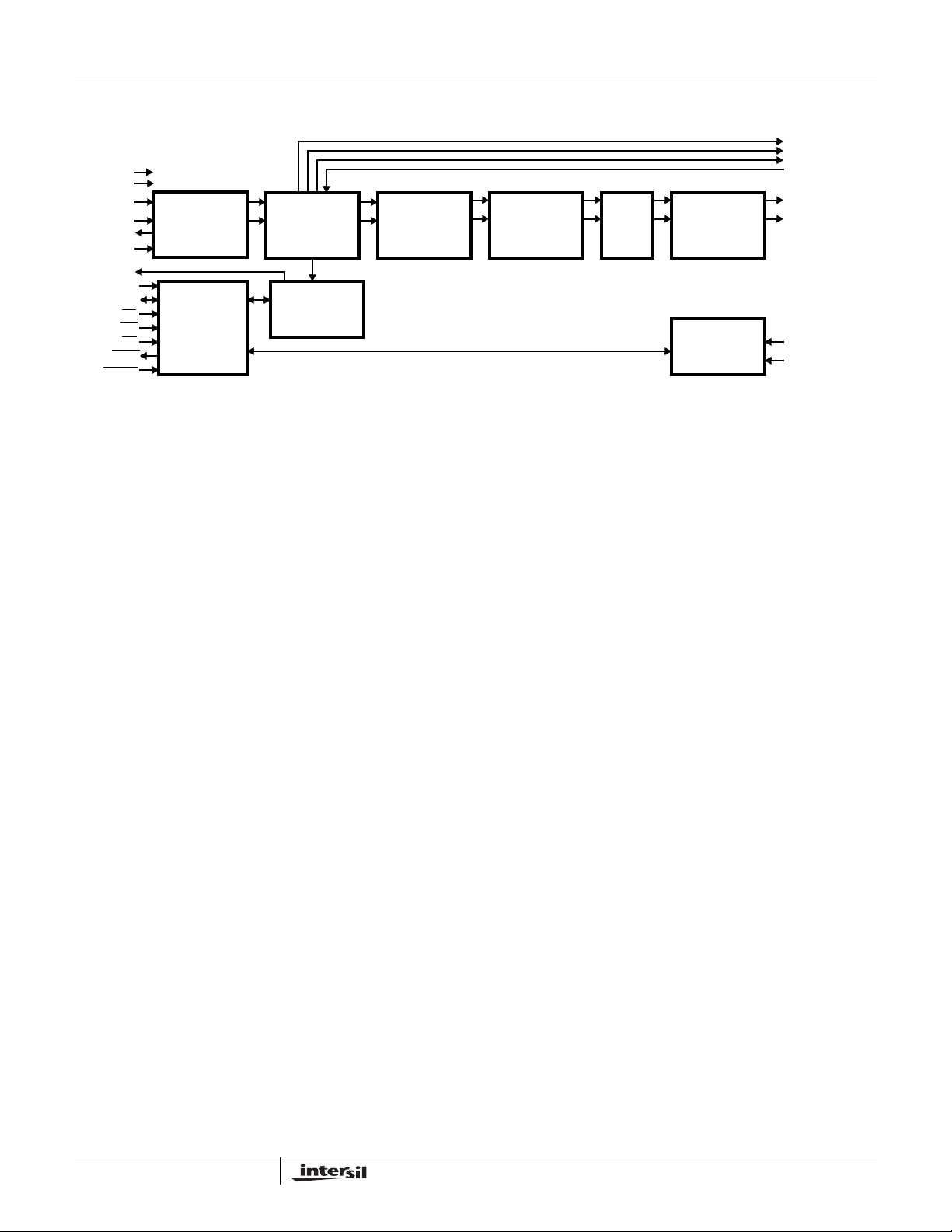
Block Diagram
www.BDTIC.com/Intersil
CLK
TRIGIN
IIN<17:0>
QIN<17:0>
CLKOUT
ISTRB
TRIGOUT
A<5:0>
P<15:0>
CS
WR
RD
BUSY
RESET
INPUT
FORMATTER
AND
INTERPOLATOR
X1, X2, X4, X8
uP INTERFACE
PRE-DISTORTER
WITH
TWO 1K x 60
LUTs
INPUT
MEMORY
(2k x 32)
ISL5239
IF CONVERTER
REAL 1X
REAL 2X
COMPLEX
CORRECTION
FILTER
REAL 1X
REAL 2X
COMPLEX
GAIN /
PHASE
OFFSET
ADJUST
OUTPUT
DAT A
FORMATTER
8-18 BIT-WIDTH
FEEDBACK
MEMORY
(1k x 20)
SERCLK
SERSYNC
SEROUT
SERIN
IOUT<17:0>
QOUT<17:0>
FBCLK
FB<19:0>
2
Page 3
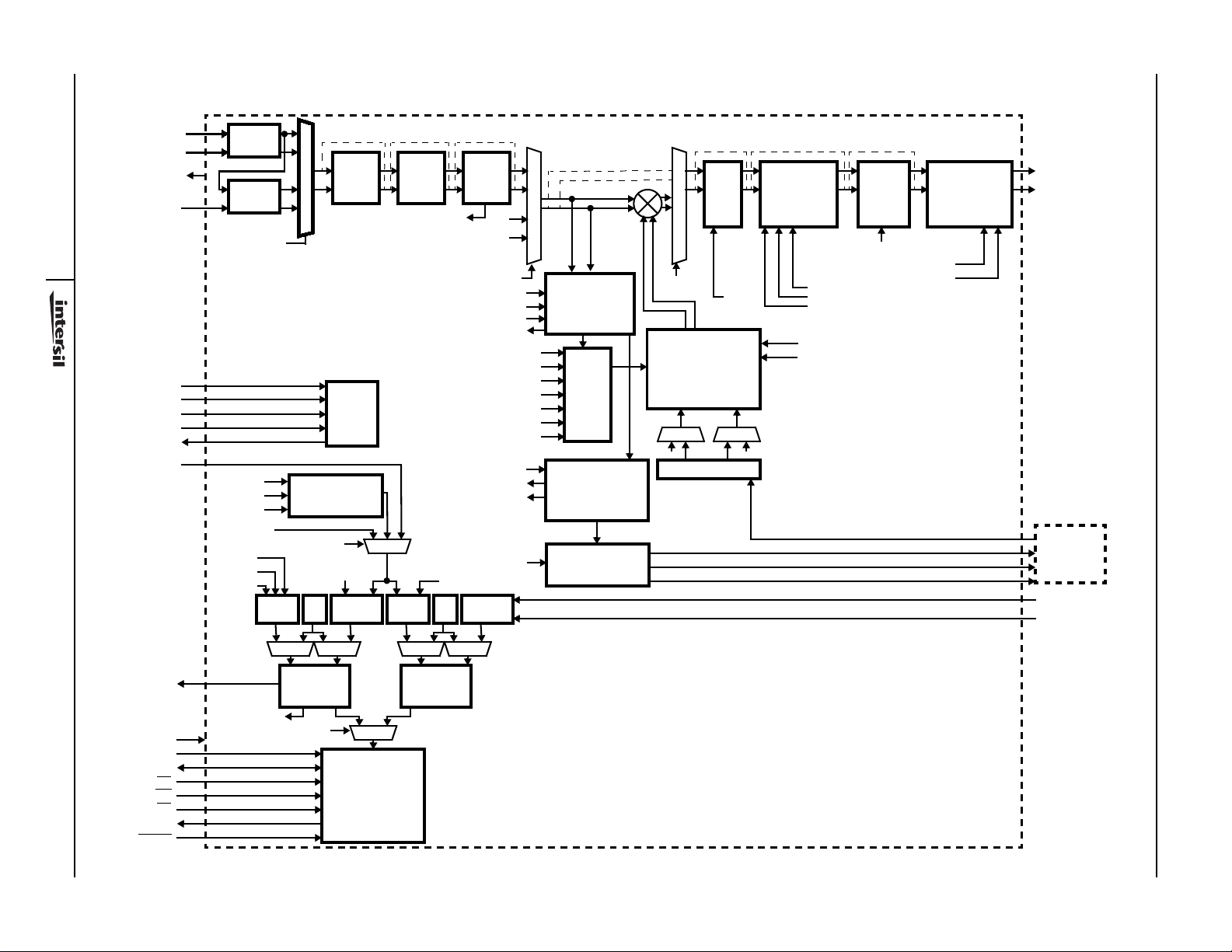
Functional Block Diagram
www.BDTIC.com/Intersil
ISL5239 Pre-Distortion Linearizer
IIN<17:0>
QIN<17:0>
CLKOUT
ISTRB
3
TMS
TDI
TCK
TRST
TDO
TRIGIN
OFFSET
BINARY
DE-MUX
INPUT TYPE
(PAR/SERIAL)
PD MAG.
MAX
IFIP I,Q
PD I,Q
PD MAG.
THRESHOLD
MIN
uP
TRIG SEL
INPUT
SEL STATE
BYPASS BYPASS BYPASS
HALF
BAND
FILTER
MUX
/
1
18
JTAG
COMPARE
INPUT DELAY
COUNT
INPUT
uP
HALF
BAND
FILTER
/ /
/
2
20
IFIP I,Q
LUT DELTA DATA Q
LUT ADDR AUTO INCR.
PWR INTGR PER.
TRIG
FB
STATE
SER. OUTPUT EN.
HALF
I
BAND
FILTER
/
20
CM TEST
FUNC. SEL.
LUT DELTA DATA I
PWR HIGH
FB DELAY COUNT
FORMAT
uP
/
Q
3
I
Q
TEST
OFFSET
SCALE
PD MAG.
LUT DATA I
LUT DATA Q
ACTIVE LUT
LUT ADDR
PWR LOW
INPUT OR TEST
LUT
ADDRESS
CALCULATION
ADDR
DATA
LUT
POWER
INTEGRATOR
PAR. TO SERIAL
BYPASS BYPASS BYPASS
IF
CONV.
PD I,Q
PRE-D OR BYPASS
BYPASS
CHANNEL 3
MEMORY EFFECT
COMPENSATION
POWER
COEF. A COEF. B
SERIAL TO PAR.
MODE
CORRECTION
FILTER
REAL 1X
REAL 2X
COMPLEX
HM, KM, LM, GM, DC OFFSETS
OUTPUT WORD WIDTH SEL.
COEF. DATA
REAL PIPELINE SEL.
COEF. ADDR.
SERIAL INPUT EN.
COEF . B SELECT
GAIN /
PHASE
OFFSET
ADJUST.
OUTPUT VALUE TYPE
OUTPUT
DATA
FORMATTER
8-18 BIT-WIDTH
SERIN
SERCLK
SERSYNC
SEROUT
IOUT<17:0>
QOUT<17:0>
EXTERNAL
MEMORY
EFFECTS
FPGA
FBCLK
FB<19:0>
ISL5239
ADDR DATA
FEEDBACK
CAPTURE
MEMORY 1K
TRIGOUT
CLK
A<5:0>
P<15:0>
CS
WR
RD
BUSY
RESET
DATA ADDR
CM TEST I,Q
MEMORY SELECT
INPUT
CAPTURE
MEMORY 2K
uP INTERFACE
Page 4
Pinout
www.BDTIC.com/Intersil
ISL5239
196 CABGA
TOP VIEW
123456789 1110
A
NC
B
NCISTRB IIN3
C
A3
A0
D
E
F
G
H
J
K
P13
L
M
N
TRST NC IOUT1
P
A1 A5 IIN13 IIN1 QOUT2 QOUT5
CS
P0
VCCC RD
P7 FB11 SERINP6
GND
TDO VCCC
NC QIN10 VCCC IOUT17
A2
QOUT17 FB17IIN10 IIN6
P1 GND
P2
P5
GND FB9
VCCIO
RESET
BUSY
TCK FB3 FB4
TMS
QIN11 IOUT16QIN4 IOUT0 IOUT2
P4
P11
P9
P15
QIN6
QIN9
QIN5 GND
QOUT11 GNDGNDQOUT15 VCCIO VCCC NCVCCC IIN16 IIN12 IIN9 IIN4 IIN0
QOUT9VCCIOVCCIOIIN17 IIN14 IIN7VCCC
VCCCQOUT12QOUT16 QOUT1 QOUT3IIN15 IIN11 IIN8 IIN2
QOUT8
QOUT13
QOUT14VCCCWR IIN5 GND QOUT10
FB13
SEROUT
SERSYNC
TRIGOUT
IOUT11GNDQIN0 VCCC
GND
VCCCIOUT9DCTEST FB2QIN2 VCCIO
VCCIO IOUT3IOUT7QIN16 GND
IOUT8QIN14 QIN3 IOUT10
QOUT6 QOUT4 NC GND
QOUT7
FB14 VCCCA4
FB16VCCIO FB15 FB10P3
GNDP10 VCCIO CLKOUTP12 P8
FB7CLK FB8P14
FB0
GNDIIOUT12
IOUT6VCCIONC IOUT14 IOUT5 VCCC NCVCCC QIN12 QIN8 QIN1 IOUT15
12
VCCIO
FB12
FB6
FB1IOUT4IOUT13QIN17TDI
VCCIO
13 14
QOUT0
FB18FB19
SERCLK
FB5
TRIGIN
FBCLKQIN15 QIN13 QIN7
POWER PIN
GROUND PIN
SIGNAL PIN
THERMAL BALL
NC (Do not connect)
Pin Descriptions
NAME TYPE DESCRIPTION
POWER SUPPLY
VCCC - Positive Device Core Power Supply Voltage, 1.8V ±0.18V.
VCCIO - Positive Device Input/Output Power Supply Voltage, 3.3V ±0.165V.
GND - Common Ground, 0V
MICROPROCESSOR INTERFACE AND CONTROL
CLK I Input Clock. Rising edge drives all of the devices synchronous operations, except feedback capture.
RESET
I Reset. (Active Low). Asserting reset will clear all configuration registers to their default values, reset all internal
states, and halt all processing.
P<15:0> I/O 16-bit bi-directional data bus that operates with A<5:0>, CS
internal control registers. When the host system asserts CS
under all other conditions, it is an input bus. Bit 15 is the MSB.
4
, RD, and WR to write to and read from the devices
and RD simultaneously, P<15:0> is an output bus,
Page 5
ISL5239
www.BDTIC.com/Intersil
Pin Descriptions (Continued)
NAME TYPE DESCRIPTION
A<5:0> I 6-bit address bus that operates with P<15:0>, CS, RD, and WR to write to and read from the devices internal
control registers. Bit 5 is the MSB.
CS
WR
RD
BUSY
EXTERNAL SERIAL INTERFACE
SERCLK O Serial Clock. Clock signal provided to external device for serial input and output, derived from rising edge of
SERSYNC O Serial Sync. Active high single-cycle pulse that is time coincident with the first sample of the 32-bit serial data
SEROUT O Serial Output. Output data bit for the serial interface. Derived from the rising edge of CLK.
SERIN I Serial Input .In put d at a bi t for se ria l int erfa ce. Derived from rising ed ge of C LK.
FEEDBACK INTERFACE
FB<19:0> I Feedback Input Data. Parallel or serial data to be stored in the feedback memory. In parallel mode, all 20-
FBCLK I Input clock used for sampling the FB<19:0> pins.
TRIGGER INTERFACE
TRIGIN I Trigger input. Hardwired trigger source to be used to trigger an input/feedback capture. Sampled internally
TRIGOUT O Trigger output. Indicated that the capture system has been triggered, either internally or externally.
DATA INPUT
IIN<17:0> I I input data. Real component of the complex input sample when input format is parallel. Alternating real and
QIN<17:0> I Q input data. Imaginary component of the complex input sample when input format is parallel. Unused in serial
ISTRB I I data strobe. (active high). Used in the muxed input format. When asserted, the input data buses contains valid
CLKOUT O Input data clock. Output clock for the data source driving the IIN<17:0> and QIN<17:0> inputs. Input data
DATA OUTPUT
IOUT<17:0> I I output data. Real component of the complex output sample driven by the rising edge of CLK. Selectable as
QOUT<17:0> I Q output data. IMaginary component of the complex output sample driven by the rising edge of CLK. Selectable
TEST ACCESS
DCTEST O DC tree output. NAND tree output for DC threshold test. Do not connect for normal operation.
JTAG TEST ACCESS PORT
TMS I JTAG Test Mode Select. Internally pulled up.
TDI I JTAG Test Data In. Internally pulled up.
TCK I JTAG Test Clock.
TRST I JTAG Test Reset (Active Low). Internally pulled-up.
TDO O JTAG Test Data Out.
I Chip Select. (active low). Enables device to respond to µP access by enabling read or write operations.
I Write Strobe, (active low). The data on P<15:0> is written to the destination selected by A<5:0> on the rising
edge of WR
I Read Strobe (Active Low). The d a t a at the ad d r e s s selected by A(5:0) i s placed on P < 1 5:0> when R D is
asserted (low) and CS
O µP Busy. (Active Low) Indicates that the µP interface is busy. The device asserts BUSY during a read operation
to indicate that the output data on P<15:0> is not ready, and it asserts this signal during a write operation to
indicate that it is not available for another read or write operation yet.
CLK.
frame. Derived from by rising edge of CLK.
bits are stored on the rising edge of FBCLK. In serial mode, bit 0 is serial input data and bit 1 is serial sync,
sampled at the rising edge of FBCLK.
with rising edge of CLK.
imaginary when input format is muxed. Selectable as 2’s complement or offset binary.
input format.
I data.
busses sampled on the rising edge of CLK that generates the rising edge of CLKOUT.
2’s complement or offset binary.
as 2’s complement or offset binary.
when CS is asserted (low).
is asserted (low).
5
Page 6
ISL5239
www.BDTIC.com/Intersil
Functional Description
The ISL5239 is a full-featured digital pre-distortion part
featuring a high-performance lookup-table based predistortion (PD) processing unit. It includes an interpolator for
upsampling and supports all varieties of upconversion
architectures with a programmable correction filter for
equalization including both sin(x)/x correction and removal of
frequency response imbalance between quadrature paths. It
also features gain, phase, and offset compensation for direct
upconversion, digital IF output for heterodyning, and
input/output capture memories with internal/external
triggering capabilities to facilitate closedloop feedback
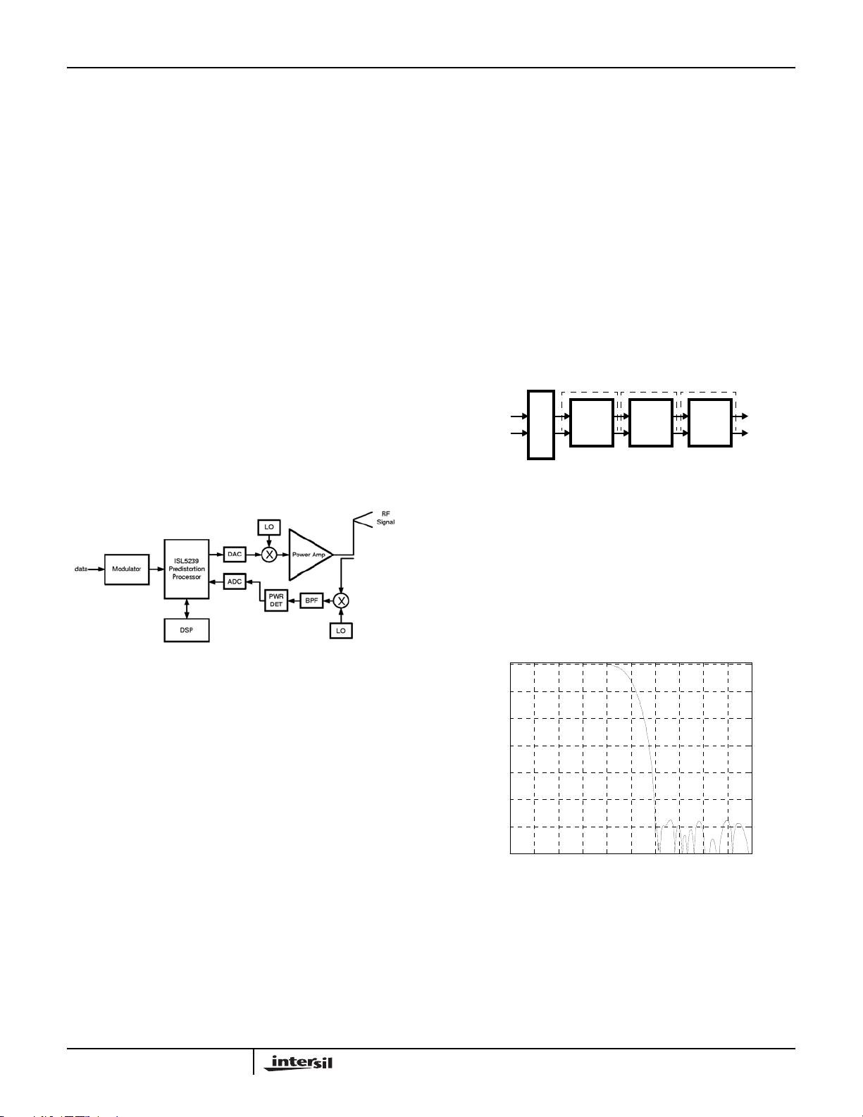
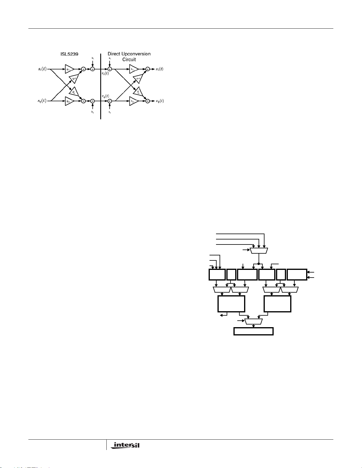
processing. System implementation is typically as shown in
Figure 1. Although the power detect feedback is shown with
one Analog to Digital Converter (ADC), coherently
demodulated feedback signalsLO configurations with 1 or 2
ADC’s are also supported.
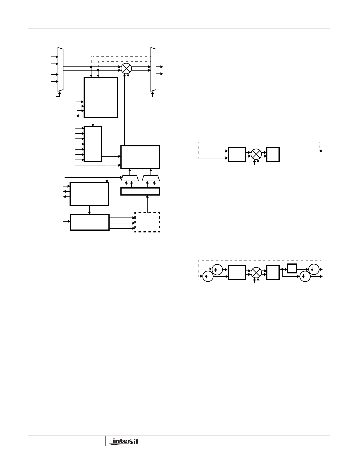
The block diagram on page 1 shows the internal functional
units within the ISL5239. In the following sections each
functional unit is described. The operation of the ISL5239 is
controlled by the register map listed in Table 3. Detailed
descriptions for each control/status register are given in
Tables 4 through 48. The control/status registers are ref erred
to in the discussion below.
The clock divider generates the CLKOUT signal which is
used to clock data from the input signal source. Typical input
sources include the ISL5217 quad programmable
upconverter, which is designed to operate seamlessly with
the ISL5239.
The interpolation factor is selectable in control word 0x02,
bits 6:4 as x1, x2, x4, and x8. The x1 mode bypasses all
three half-band filters. The x2 mode utilized HB1 and
bypasses HB2 and HB3. The x4 mode utilized HB1 and HB2
and bypasses HB3. Finally, the x8 mode utilizes all three
HBFs. Saturation status bits are provided for each of the
three HBFs in the status register 0x03.
Input data rates up to the CLK rate are supported, based on
the requirement CLK >= Fs * IP, where Fs is the input rate of
the incoming data and IP is the interpolation factor selected
in control word 0x02.
/
1
20
BYPASS BYPASS
HALF
BAND
FILTER
2
20
/
HALF
BAND
FILTER
3
I
Q
/
20
BYPASS
IIN<17:0>
QIN<17:0>
FIGURE 2. INPUT FORMATTER AND INTERPOLAT OR
BLOCK DIAGRAM
HALF
BAND
FILTER
/
INPUT
18
FORMATTER
FIGURE 1. SYSTEM OVERVIEW
Input Formatter and Interpolator (IFIP)
The Input Formatter and Interpolator interfaces to the data
source to provide for parallel data input via the IIN<17:0>,
QIN<17:0> busses, or serial input via the IIN<17:0> input
bus. In parallel input mode, both 18-bit input busses are
used to allow for parallel I and Q sample loading. In serial
mode, the data is input via the IIN<17:0> bus only, as the I
sample followed by the Q sample with the ISTRB input
asserted with each I sample. In this mode, the QIN<17:0>
bus is not utilized. The input data format is selectable as
either two’s complement or offset binary.
The Interpolator function is necessary because predistorting a signal results in a much wider bandwidth signal
(typically 5x to 7x wider). The Input Formatter and
Interpolator is depicted in Figure 2.
Each half-band filter performs a x2 interpolation by inserting
one zero between each input data sample, causing the
sampling frequency to double. The resulting zero-stuffed
data is then low pass filtered to reject the upsampling image.
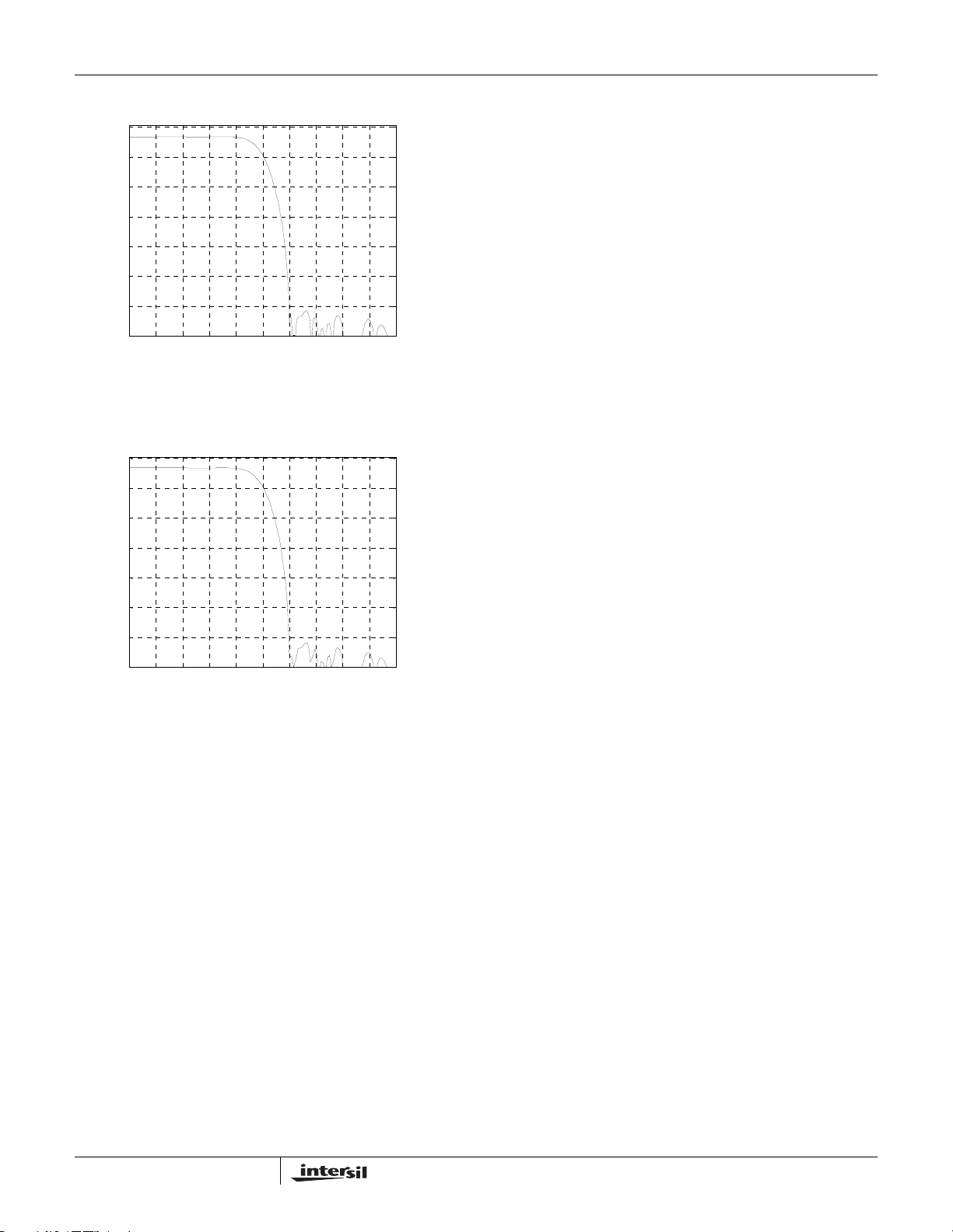
The half-band filter frequency responses are as shown in
Figure 3.
0
-20
-40
-60
-80
MAGNITUDE (dB)
-100
-120
-140
FIGURE 3. x2, HB1 ENABLED FREQUENCY RESPONSE
HALFBAND FILTER 1 RESPONSE
0 0.1 0.2 0.3 0.4 0. 5 0.6 0.7 0.8 0.9 1
NORMALIZED FREQUENCY (NYQUIST=1)
Three interpolation rates (x2, x4, and x8) are supported by
the cascade of three Half-Band (HB) Filters. The ISL5239
includes an on-chip clock divider to facilitate input clocking.
6
Page 7
ISL5239
www.BDTIC.com/Intersil
0
-20
-40
-60
-80
MAGNITUDE (dB)
-100
-120
-140
FIGURE 3A. X4, HB1 AND HB2 ENABLED FREQUENCY
0
-20
-40
-60
-80
MAGNITUDE (dB)
-100
-120
-140
FIGURE 3B. X8, HB1-HB3 ENABLED FREQUENCY RESPONSE
HALFBAND FILTER 2 RESPONSE
0 0.1 0.2 0.3 0.4 0. 5 0.6 0.7 0.8 0.9 1
NORMALIZED FREQUENCY (NYQUIST=1)
RESPONSE
HALFBAND FILTER 3 RESPONSE
0 0.1 0.2 0.3 0.4 0. 5 0.6 0.7 0.8 0.9 1
NORMALIZED FREQUENCY (NYQUIST=1)
Pre-Distorter (PD)
The function of the Pre-distorter is to compute the
magnitude of the input signal, look up a complex distortion
vector based on the magnitude, and apply that distortion to
the input signal.
The signal magnitude may be computed by any of three
different methods: log of power, linear magnitude or linear
power. The result is scaled and offset by programmable
amounts and becomes the address into a Look-up Table
(LUT).
Two LUTs are available, one of which is ‘live’ in the circuit
and the other is offline and can be loaded via the processor
interface. This configuration allo ws instantaneou s s witching
of pre-distortion characteristics without unpredictable
effects on the processed signal.
The LUTs contain a complex distortion vector, as well as
complex delta values which interact with an external
Thermal/Memory calculation circuit to predict the effects of
temperature changes on the RF amplifier’s behavior and
compensate. The average power into the amplifier is
computed and transmitted serially off chip. The external
circuits compute one or two memory effect coefficients
which are combined with the complex delta values in the
LUT to derive the final distortion vector. The distortion
vector is a rectangular complex value which is multiplied
with the input signal resulting in a magnitude based nonlinearity. Access to the LUT is optimized by the use of an
auto incrementing address register which allows the tables
to be updated with only one address register write
operation. Control words 0x10 through 0x1d apply to the
7
Page 8
ISL5239
www.BDTIC.com/Intersil
pre-distorter. The pre-distorter block diagram is shown in
Figure 4.
FROM
I
IFIP
Q
CM TEST
LUT ADDR AUTO INCR.
SERIAL INPUT EN.
PWR INTGR PER.
SER. OUTPUT EN.
I
Q
INPUT OR TEST
TEST
FUNC. SEL.
OFFSET
SCALE
PD MAG.
LUT DATA I
LUT DATA Q
LUT DELTA DATA I
LUT DELTA DATA Q
ACTIVE LUT
LUT ADDR
COEF. B SELECT
PWR LOW
PWR HIGH
LUT
ADDRESS
CALCULATION
POWER
ADDR
LUT
DATA
POWER
INTEGRATOR
PAR. TO SERIAL
BYPASS
MEMORY EFFECT
COMPENSATION
COEF. A COEF. B
SERIAL TO PAR.
SERCLK
SERSYNC
SEROUT
EXTERNAL
MEMORY
EFFECTS
FPGA
I
Q
PRE-D OR BYPASS
SERIN
FIGURE 4. PRE-DISTORTER BLOCK DIAGRAM
Serial Interface
The serial interface for the external memory effects
calculation consists of outputs SERCLK, SERSYNC, and
SEROUT and input SERIN. The serial output sends the 32bit unsigned average power off-chip for further processing.
The data is transmitted via the SEROUT pin MSB first, with
the first bit marked by a high pulse on the SERSYNC pin.
The SERCLK rate is scaled such that 32 bits are transmitted
in one period of the power integrator as controlled by register
0x18 bits 5:4. SEROUT is enabled by register 0x18 bit 12.
IF Converter (IFC)
The output of the pre-distorter is a complex baseband signal
sampled at the system CLK rate. To provide greater system
flexibility, the IF Converter function can change this in one of
three different ways, providing frequency shifts, sample rate
changes and complex to real conversions.
Real 1X
The real 1x operating mode shifts the signal up by Fs/4 and
performs a complex to real conversion without changing the
base sample rate. This mode has 1/2 the bandwidth of the
original input signal, with the I output channel active and the
Q output channel set to 0. The operation of the IF converter
in this mode is shown in Figure 5.
BYPASS
I
Q
FROM
PD
FIGURE 5. IF CONVERTER IN REAL 1X MODE OPERATION
Real 2X
The real 2x operating mode converts complex to real at 2x
the sample rate and shifts the signal up to Fs/2 (Fs/4 of the
output rate). This mode has the same bandwidth as the
original signal with the I channel carrying the first of twwo
samples/clock and the Q channel carrying the second
sample. The operation of the IF Converter in this mode is
shown in Figure 6.
I
Q
FROM
2
PD
FIGURE 6. IF CONVERTER IN REAL 2X MODE OPERATION
HALF
BAND
FILTER
j(pi/2)(n)
e
BYPASS
HALF
2
BAND
FILTER
j(pi/2)(n)
e
Re{*}
Re{*}
-1
Z
2
I
I
2
Q
The SERIN receives the thermal compensation parameters
from external processing using the same SERCLK and
SERSYNC used by the SEROUT. The chip expects to
receive 32 bits of data sequentially on the SERIN pin: the
MSB of A, followed by the rest of A, then the MSB of B,
followed by the rest of B. The SERIN is enabled by register
0x18 bit 8. When SERIN is disabled, registers 0x19 and
0x1a supply the A and B parameters for the thermal
compensation calculations. See Figure 16 for a detailed
timing diagram of the serial interface.
8
Page 9
ISL5239
www.BDTIC.com/Intersil
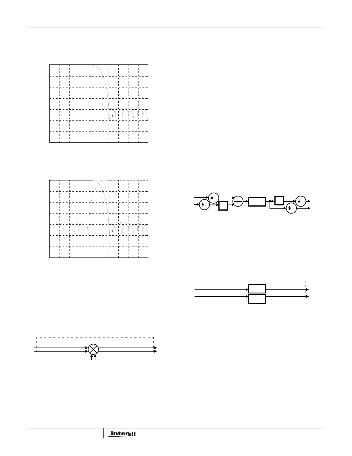
The IF converter frequency response is as shown in
Figure 7, with the folding effect shown in Figure 7A for the
x2, Fs/4 upconverter case.
0
-20
-40
-60
-80
MAGNITUDE (dB)
-100
-120
-140
0
-20
-40
-60
IFC FILTER RESPONSE (x2 MODE)
0 0.1 0.2 0.3 0.4 0. 5 0.6 0.7 0.8 0.9 1
NORMALIZED FREQUENCY (NYQUIST=1)
FIGURE 7. x2, IFC FREQUENCY RESPONSE
IFC FILTER RESPONSE (x2 MODE, WITH FOLDING)
Correction Filter (CF)
To compensate for imperfections in the analog filtering which
takes place after D/A conversion, the correction filter
provides an independent 13-tap FIR filter on each channel.
These filters may be programmed to remove differential
group delay and ripple characteristics of external analog
circuits including sin(x)/x correction and frequency response
imbalance between the I and Q channels using either
amplitude or group delay. This allows for correction of the
two physically separate I and Q analog response paths from
the DAC’s through the quadrature up-converter. It also
provides correction of the bandpass response when
operating in a complex frequency shifted IF mode. There are
two possible correction fi lter modes.
Real 2X
When the IF Converter is set to generate 2x sampled real
data, the Correction Filter must be reconfigured to process
this data correctly. In this mode it effectively pro vides one 13tap block-mode filter when the coefficients for the two filters
are programmed identically.
BYPASS
I
Q
FROM
IFC
2
2
-1
Z
I/Q FIRs
-1
Z
2
I
2
Q
-80
MAGNITUDE (dB)
-100
-120
-140
0 0.1 0.2 0.3 0.4 0. 5 0.6 0.7 0.8 0.9 1
NORMALIZED FREQUENCY (NYQUIST=1)
FIGURE 7A. x2, IFC FREQUENCY RESP. WITH FOLDING
Complex
The complex operating mode simply shifts the complex
baseband signal up by Fs/4 without any filtering or real
conversion. The operation of the IF converter in this mode is
shown in Figure 8.
BYPASS
I
Q
FROM
PD
j(pi/2)(n)
e
FIGURE 8. IF CONVERTER IN COMPLEX MODE OPERATION
I
Q
FIGURE 9. CORRECTION FILTER IN REAL 2X MODE
Complex or Real 1x
When configured for operation in the complex mode, one 13tap filter is provided for each the I and Q channels. In Real 1x
mode, the Q channel is not used.
BYPASS
I
Q
FROM
IFC
I-CHAN
FIR
Q-CHAN
FIR
FIGURE 10. CORRECTION FILTER IN COMPLEX MODE
I
Q
Output Data Conditioner (ODC)
The Output Data Conditioner can apply I/Q balance
corrections, DC offset corrections and output format
conversions.
To compensate for gain/phase imperfections in external
analog modulation circuits which can result in poor image
rejection and reduced dynamic range, the ODC provides an
I/Q balance corrector. The I/Q balance corrector provides
four coefficients to control the magnitude of the direct and
9
Page 10
ISL5239
www.BDTIC.com/Intersil
cross-coupled term on both the I and Q channels. Typical
implementation is as shown in Figure 10.
FIGURE 11. IMBALANCE CORRECTION
The Output formatter also provides DC offset correction to
1/4 LSB for 18-bit outputs to reduce analog DC offsets
introduced in external D/A conversion and modulation
circuits which can degrade system performance by causing
carrier feed through in complex baseband systems, or spurs
at DC for IF systems.
The ODC also provides programmable output precision 8 to
18-bits, with unbiased (convergent) rounding, since practical
system designs will require D/A converters with fewer than
18-bits. Internal accuracy is in excess of 18-bits, and utilizes
20-bit data paths in critical areas. Additionally, both two’s
complement and offset binary formats are supported.
Capture Memory (CM)
The Capture Memory allows the capture and viewing of data
from various points in the chip. The primary function is to
capture the digital signals coming into the pre-distorter. The
CM also provides a secondary mode, as it can provide
stimulus directly to the pre-Distorter. The CM is comprised of
both the Input and the Feedback Memories. The processor
interface provides the access to view, input, and alter the
memory data. Synchronized (triggered) capture of both input
and feedback signals is a typical requirement of adaptive
digital pre-distortion systems.
Input Memory
The input capture memory observes the signals going into
the amplifier. The 2K deep memory grabs complex samples
of data at one of three possible locations, either at the input
to the pre-distorter, the output of the pre-distorter, or from its
magnitude calculation. In addition to capturing input data,
this memory may also be configured as a data source. The
input capture memory may be pre-loaded with user defined
data and ‘played’ into the pre-distorter to stimulate the
system with signals that will elicit a desired response.
Feedback Memory
The feedback memory allows the user to capture data from
an external system and to view the memory through the
processor interface. The feedback memory is used to
observe the signals coming out of the amplifier. The 1K deep
memory grabs 20-bit data, either in parallel or serial format.
The feedback capture memory has its own clock input,
FBCLK, which must be synchronously derived from CLK and
meet the timing requirements.
Capture operations may be triggered by an external signal
(TRIGIN), by magnitude threshold crossings detection
programmed in the magnitude threshold maximum and
minimum values, or by system software writing to the
processor trigger bit in control word 0x04, bit 6. Separate
programmable delays of up to 32k samples are provided for
both input memory and feedback capture, allowing system
delays to be calibrated out for optimum alignment prior to
analysis. A TRIGOUT output is provided to indicates when a
capture operation has begun.
The processor interface to the capture memories is designed
to minimize the time required for loading/unloading. Although
access to the memories takes place through indirect address
and data registers, auto incrementing of the address is
supported so the address only needs to be written once to
access the entire memory. The capture memory is as shown
in Figure 13.
TRIGIN
MAG COMP
uP
IFC I,Q
PD I,Q
PD MAG
CM TEST I,Q
MEMORY SELECT
TRIG SEL
INPUT DELAY
COUNT
INPUT
uP
SEL STATE
DATA ADDR
INPUT
CAPTURE
MEMORY 2K
FIGURE 12. CAPTURE MEMORY BLOCK DIAGRAM
TRIG
INPUT
uP INTERFACE
STATE
FB DELAY COUNT
FB
uP
ADDR DATA
FEEDBACK
CAPTURE
MEMORY 1K
FORMAT
FBCLK
FB<19:0>
Memory Modes and Programming Instructions
Unless noted, the following discussion applies to both the
input memory and feedback memory operations. Prior to
invoking the memory to capture or send data, the control
word 0x06, bits 14:0 input trigger delay counter, 0x08 bits
14:0 feedback trigger delay count, 0x05, bits 10:0 input
length, 0x04, bits 2:1 input memory datain source or 0x04,
bit 8 feedback input format, and 0x04, bits 5:4 trigger select
registers must be loaded.
10
Page 11

ISL5239
www.BDTIC.com/Intersil
For the input data, the 0x04, bit 3 input data round bit must
also be selected and the feedback memory length count is
always set to 1024. To invoke memory operation, the 0x07,
bit 4 feedback memory mode or bits 1:0 input memory mode
and 0x04, bit 6 processor trigger must be controlled.
There are three modes of operation — capture, loop, and
single-shot. The feedback memory does not have a loop
mode. A synopsis of the three modes is described below.
Capture Mode
There are two types of capture mode — advanced trigger
and single/capture. The advanced trigger mode allows data
to be captured around a trigger point, and the quantity of the
data captured after the trigger point is set by 0x06, bits 14:0.
When input memory capture mode = DELAY, the delay
register acts as a delay count prior to the capture or sending
of data. The max delay in this case is 32768 counts or
system clock ticks. The advanced trigger mode is used in
capture mode only. With the feedback capture operations
being analogous to the input memory , one feedbac k memory
exception is its control register 0x08, bits 14:0. It has 10
LSBs of available capture space.
Advanced Trigger Capture Mode Sequence
The control register 0x0e, bit 13:12 input capture status,
should be in IDLE. Set 0x06, bit 15, input memory capture
mode to ADVANCE to signify an advanced trigger capture.
0x06, bits 14:0 set the input trigger delay counter to = 0x56
signifies there are 86 points captured after the occurrence of
the trigger point, 0x0e, bit 10:0, input trigger position and all
other points are captured prior to trigger point. Note: only the
11 lsbs are valid for the delay capture in this mode. The input
trigger position is a read-only register and adding to it the 11
lsbs of the input trigger delay counter determines the
position of the final data point captured after the trigger. If the
input trigger position is 0x1ff, the final point captured
occurred at address: 0x1ff + 0x56 = 0x255 or 597 (decimal).
The user must set the input trigger delay counter prior to
invoking the transaction of the capture.
The user invokes the capture mode register by writing
CAPTURE to 0x07, bit 1:0 input memory mode. The system
is in the advanced trigger capture mode and 0x0e, bits
13:12, input capture status is ARMED. The system waits for
a trigger as the memory is continuously being written into.
When a trigger occurs, the trigger causes the memory to
load the data till the memory address is equal to input trigger
position + 11 lsbs of the input trigger delay counter. The
memory address that is time coincident with the trigger
occurrence latches to the input trigger position. During this
period, the input capture status is LOADING. When the final
capture point loads, the input capture status returns to IDLE
and a new capture transaction can be initiated by writing
CAPTURE to the input memory mode.
Single/Capture Mode
The sequence for the single shot stimulus mode, input
memory mode = SINGLE, and input memory capture mode
= CAPTURE with input capture mode = DELAY are the
identical. The function of the memory reading or writing
provides the difference between the two modes. In the single
shot case, the capture memories read data to the output bus,
and in the capture mode, they write data to the memories.
The sequence of operation in the Single/Capture mode is
described below.
The input capture status should be in IDLE and the input
memory capture mode in DELAY with the input memory
delay counter set to 0x0056. Note: The 15 LSBs of the input
memory delay counter are valid for the delay count in this
mode. After the trigger, Ox56 signifies there are 86 counts of
delay before the start of the capture/send of data to/from the
memory.
The user invokes the capture mode by writing the input
memory mode to CAPTURE. The system is in the capture
mode and the input memory status is ARMED. The system
waits for a trigger and the memory is idle at this point. When
a trigger occurs, the trigger causes the delay counters to
count 86 clocks of delay. At the end of the delay, the
memories begin their writing sequence until input memory
length data points are written. During the writing of data, the
input memory status is LOADING. When the final input
memory length point is written, the input memory status
returns to IDLE and a new capture transaction can be
initiated by writing CAPTURE to the input memory mode.
For the Single Capture mode, the deviations from the
sequence are the writing of the input memory mode to
SINGLE, and the input memory status to SEND when
reading of the data from memory. All other operations are
analogous.
Loop Mode
This is a continuous play mode from the memories;
therefore, the memories should contain valid data before
invoking transactions. The length of each repeatable output
stream is controlled by the input memory length. Upon
outputting the final input memory length point, the hardware
resets to play another set of input memory length points from
the memory.
The user invokes the loop mode by writing input memory
mode to LOOP. The system is in the loop mode and the input
memory status = SEND. The memory starts reading data
continuously and a stop can be initiated by setting input
memory mode to IDLE during the transaction. The input
memory status returns to IDLE and a new loop transaction
can be initiated by writing the input memory mode to LOOP.
This is the only mode where immediate mode changes are
acknowledged during its transaction cycle.
11
Page 12

ISL5239
www.BDTIC.com/Intersil
General Comments About Modes
Once a trigger is detected in the ARMED condition, all
following triggers are ignored during the sequence. The
system does not acknowledge new triggers until a new
transaction is invoked and re-armed. When a new mode is
invoked, all subsequent inv ocations of new modes during the
duration of its sequence is ignored, except in the loop mode.
In the loop mode, an input memory mode change to IDLE is
processed immediately.
When in the IDLE, all controls, addresses, and data, default
to the processor interface values.
Triggers
When a capture memory is ARMED, i.e. waiting for a trigger
to happen, the activation of the trigger occurs in three ways
— external, data dependent, and user invoked. The trigger
select, 0x04, bits 5:4, provides the selection of the trigger
source. When the pre-distorter magnitude bus values fall
between the range of 0x09 minimum and 0x0a maximum,
the data dependent trigger activates. The first of these
transitions causes a trigger to be detected and the remaining
triggers during the capture sequence is ignored.
To invoke the user invoked trigger, 0x04, 5:4, set to
processor, the programmer writes a TRIGGER to the 0x04,
bit 6 processor trigger register. After a TRIGGER is in the
field, the user initiates the trigger by just writing to that
register. The user does not have to reset the trigger back to
IDLE. By setting the processor trigger bit to IDLE when not in
use, it keeps the circuit quiet and allows the user to write to
other values at that address without causing a trigger to
occur during operation. To disable the processor trigger, the
user should change trigger select to something other than
PROCESSOR and then change values in processor trigger.
If trigger select is not set to PROCESSOR, the system
ignores the trigger generated by processor trigger.
The feedback and input memory circuit uses the same
trigger; both circuits trigger at the same point with its
operation registers causing different operations to occur. The
user should monitor input memory status and feedback
memory status simultaneously before activating triggers.
Make sure both status registers are in ARMED before
activating triggers or the results from the capture can be
erroneous and data can be overwritten. Selecting processor
trigger (register 0x04, bits 5:4 = 00) while arming the input
and feedback memory circuits is a convenient way to ensure
no unexpected triggers occur before confirming ARMED
status of both circuits.
Input Data to Input Memory
There are three sources of input data to the input memory —
interpolator, pre-distorter’s data outputs, and the predistorter’s magnitude. Data from the interpolator and the
predistort output are the upper 16 bits with or without
rounding. Only 16 of the original 20 bits of I or Q is loaded
into the memory. The I data is read from the memory on the
DataHigh register and the Q data, DataLow register.
In the predistort magnitude input, the data is unsigned 16
bits and the software has to reshuffle the data to extract the
original magnitude. The DataHigh contains only the predistorter magnitude bit 15, and the DataLow contains the
pre-distorter magnitude 14:0.
Writing/Reading the Memories from the Proc essor
Interface
In the auto-increment mode, the data is loaded in 16-bit
increments. The low word is written or read first followed by
the high word. The high word increments the address
counter and generates the actual write to the memory. For
reading, it just increments the counter. The input memory
select 0x04, bit 12, selects the memory to be written to or
read from.
When writing or reading a specific address, the 0x0b
address register must be loaded before the 0x0c and 0x0d
memory data registers. In the write, the high word
transaction will trigger the actual write to the memory and a
low word must be written first. For additional details, see the
uP interface section.
Microprocessor Interface
The microprocessor interface allows the ISL5239 to appear
as a memory mapped peripheral to the µP. All registers can
be accessed through this interface. The interface consists of
a 16 bit bidirectional data bus, P<15:0>, six bit address bus,
A<5:0>, a write strobe (WR
enable (CE
and write strobe inputs.
The processor interface provides a simple parallel
Data/Control/Address bus for monitoring and controlling its
operation. The processor interface is asynchronous to the
CLK, and BUSY signal is included to indicate when read and
write operations are complete.
The register configuration is master/slave, where the slave
registers are updated from the masters and all reads access
the slaves.
The master registers are clocked by the µP WR
writable and cleared by a hard reset. The slave registers are
clocked by CLK, and are readable and cleared by either a
hard or soft reset. The transfer of configuration data from the
master register to the slave register occurs synchronously
after an event and requires a four clock synchronization
period.
The µP can perform back-to-back accesses to the register,
but must maintain four f
the same address. This limits the maximum µP access rate
for the RAM to 125MHz/4 = 31.25MHz.
). The interface is configured for separate read
), a read strobe (RD) and a chip
strobe, are
periods between accesses to
CLK
12
Page 13

ISL5239
www.BDTIC.com/Intersil
The address map and bit field details for the microprocessor
interface is shown in the Tables 2-48. The procedures for
reading and writing to this interface are provided below.
Microprocessor Read/Write Procedure
The ISL5239 offers the user microprocessor read/write
access to all of the configuration registers and the capture
memory.
Configuration Read/Write Procedure
Write Access to the Configuration Master
Registers
Perform a direct write to the configurati on master registers
by setting up the address A<5:0>, data P<15:0>, enabling the
CS
input, and generating WR strobe. The rising edge of the
WR
initiates the transfer to the master register. Registers may
be written in any order.
1. Write the global control register 0x00.
2. Write all remaining registers sequentially .
3. Load all IFIP, PD, IFC, CM and ODC coefficients and
control words.
RD
WR
A<5:0> 0x00
P<15:0>
FIGURE 13. CONFIGURATION WRITE TRANSFER
0x01 0x02 0x03
xxxx
0x04 0x05
Read Access to the Configuration Slave Registers
1. Perf orm a direct read of a configuration register by
dropping the RD line low to transfer data from the register
selected by A<5:0> onto the data bus P<15:0>.
RD
WR
A<5:0>
P<15:0>
FIGURE 14. CONFIGURATION READ TRANSFER
0X00 0X01 0X02 0X03 0X04 0X05
HI-Z
DATA VALID
LUT Read/Write Procedure
Write Access to the LUT Memory
1. Perf orm a direct write to control word 0x13 by setting up
the address on A<5:0>, data on P<15:0>, and generating
a rising edge on WR.
mode and the LUT address as specified in bit 9:0.
2. Perf orm a direct write to any/all control words 0x14, 0x15,
or 0x16, in any order, by setting up the address on A<5:0>,
data on P<15:0>, and generating a rising edge on WR.
0x13 selects the auto increment
3. Perf orm a direct write to control word 0x17 by settin g u p
the address on A<5:0>, data on P<15:0>, and generating
a rising edge on WR. The WR updates the contents of
0x014-0x017 and performs the auto increment, if
enabled.
Read Access to the LUT
1. Perf orm a direct write to control word 0x13 by settin g u p
the address on A<5:0>, data on P<15:0>, and generating
a rising edge on WR.
mode and the LUT address as specified in bit 9:0.
2. Perf orm a direct read of any/all control words 0x14, 0x15,
0x16, in any order, by dropping the RD line low to transfe r
data from the slave register selected by A<5:0> onto the
data bus P<15:0>.
3. Perf orm a direct read of control word 0x17 by dropping the
line low to transfer data from the slave register
RD
selected by A<5:0> onto the data bus P<15:0> . Reading
from this control word performs the auto increment, if
enabled.
0x13 selects the auto increment
Capture Memory Read/Write Procedure
Indirect addressing is used to access the Capture Memory.
The control word 0x04, bit 12 selects whether the input or
feedback memory is accessed and bit 13 selects the auto
address increment or manual modes. Control word 0x0b is
the memory address, and words 0x0c and 0x0d combine to
form the 32-bit word which is written or read from the
memory. The write to 0x0d triggers the write to the memory
and the auto increment of the address, if enabled. When
reading feedback capture memory , 0x0c bits 3:0 will contain
the upper four bits, and 0x0d, bits 15:0 will be the remaining
15-bits.
Write Access to the Capture Memory
1. Perf orm a direct write to control word 0x04 by settin g u p
the address on A<5:0>, data on P<15:0>, and generating
a rising edge on WR.
mode and the input or feedback memories.
2. Perf orm a direct write to control word 0x0b by settin g u p
the address on A<5:0>, data on P<15:0>, and generating
a rising edge on WR. 0x0b selects the starting memory
address.
3. Perform a direct write to 0x0c by setting up the address on
A<5:0>, data on P<15:0>, and generating a rising edge on
WR.
4. Perf orm a direct write to control word 0x0d by settin g u p
the address on A<5:0>, data on P<15:0>, and generating
a rising edge on WR.
0x0c and 0x0d and performs the auto increment, if
enabled.
0x04 selects the auto increment
The WR updates the contents of
13
Page 14

ISL5239
www.BDTIC.com/Intersil
Read Access to the Capture Memory
1. Perf orm a direct write to control word 0x04 by setting up
the address on A<5:0>, data on P<15:0>, and generating
a rising edge on WR. 0x04 selects the auto increment
mode and the input or feedback memories.
2. Perf orm a direct read of 0x0c by dropping the RD line low
to transfer data from the slave register selected by
A<5:0> onto the data bus P<15:0>.
3. Perf orm a direct read of control word 0x0d by dropping the
line low to transfer data from the slave register
RD
selected by A<5:0> onto the data bus P<15:0>. Reading
from this control word performs the auto increment, if
enabled.
Correction Filter Read/Write Procedure
Write Access to the Correction Filter Coefficients
1. Perf orm a direct write to control word 0x28 by setting up
the address on A<5:0>, data on P<15:0>, and generating
a rising edge on WR.
mode.
2. Perf orm a direct write to control word 0x29 by setting up
the address on A<5:0>, data on P<15:0>, and generating
a rising edge on WR. 0x29 selects the coefficient address
for I or Q.
3. Perf orm a direct write to control word 0x2a by setting up
the address on A<5:0>, data on P<15:0>, and generating
a rising edge on WR.
4. Repeat step 3 until all 13 coefficients for I and for Q hav e
been loaded as the master registers are transferred to the
slaves when the last Q coefficient is written.
0x28 selects the auto increment
Read Access to the Correction Filter Coefficients
1. Perf orm a direct write to control word 0x028 by settin g up
the address on A<5:0>, data on P<15:0>, and generating
a rising edge on WR.
mode.
2. Perf orm a direct write to control word 0x029 by settin g up
the address on A<5:0>, data on P<15:0>, and generating
a rising edge on WR.
3. Perf orm a direct read of 0x2a by dropping the RD line low
to transfer data from the slave register selected by
A<5:0> onto the data bus P<15:0>.
0x28 selects the auto increment
Latency
To be provided later.
Reset
There are three types of chip resets.
RESET pin
A hard reset can occur by asserting the input pin RESET
which resets all chip registers to their default condition, and
resets the uP interface.
Software Hard Reset
The µP can issue a reset command through the global
control register 0x00, bit 4. This reset is identical to asserting
the RESET
not affected, and the uP interface is not reset.
pin, except the control fields 0x00 and 0x01 are
Software Soft Reset
The uP can issue a reset command through the global
control register 0x00, bit 0, which is identical to a Software
hard reset, but none of the control registers are reset. A soft
reset leaves the device in an idle state.
JTAG Test
The IEEE 1149.1 Joint Test Action Group boundary scan
standard operational codes shown in Table 9 are supported.
A separate application note is available with implementation
details and the BSDL file is available.
TABLE 1. JTAG OP CODES SUPPORTED
INSTRUCTION OP CODE
EXTEST 0000
IDCODE 0001
SAMPLE/PRELOAD 0010
INTEST 0011
BYPASS 1111
Power-up Sequencing
The ISL5239 core and I/O blocks are isolated by structures
which may become forward biased if the supply voltages are
not at specified levels. During the power-up and power-down
operations, differences in the starting point and ramp rates of
the two supplies may cause current to flow in the isolation
structures which, when prolonged and excessive, can
reduce the usable life of the device. In general, the most
preferred case would be to power-up or down the core and
I/O structures simultaneously. However, it is also safe to
power-up the core prior to the I/O block if simultaneous
application of the supplies is not possible. In this case, the
I/O voltage should be applied within 10 ms to 100 ms
nominally to preserve component reliability. Bringing the
core and I/O supplies to their respective regulation levels in
a maximum time frame of a 100 ms, moderates the stresses
placed on both, the power supply and the ISL5239. When
powering down, simultaneous removal is preferred, but It is
also safe to remove the I/O supply prior to the core supply. If
the core power is removed first, the I/O supply should also
be removed within 10-100mS.
Application Notes and Evaluation Boards
The ISL5239 operation can be demonstrated via the
ISL5239EVAL1 board. All required hardware and Windows
GUI software are supplied with both a user’s manual and
accompanying applications notes.
14
Page 15

ISL5239
www.BDTIC.com/Intersil
Absolute Maximum Ratings Thermal Information
Supply Voltage. . . . . . . . . . . . . . . . . . . . . . +2.5VCCC, 4.6V VCCIO
Input, Output or I/O Voltage. . . . . . . . . . . . . . . . .GND -0.5V to 5.5V
ESD Classification . . . . . . . . . . . . . . . . . . . . . . . . . . . . . . . . .Class 2
Operating Conditions
Voltage Range Core, V
Voltage Range I/O, V
Temperature Range
Industrial. . . . . . . . . . . . . . . . . . . . . . . . . . . . . . . -40
Input Low Voltage . . . . . . . . . . . . . . . . . . . . . . . . . . . . . 0V to +0.8V
Input High Voltage . . . . . . . . . . . . . . . . . . . . . . . . . . . . . . .2V to V
CAUTION: Stresses above those listed in “Absolute Maximum Ratings” may cause permanent damage to the device. This is a stress only rating and operation of the
device at these or any other conditions above those indicated in the operational sections of this specification is not implied.
NOTES:
is measured in free air with the component mounted on a high effective thermal conductivity test board. See Tech Brief TB379.
1. θ
JA
2. With “direct attach” features (i.e., vias in the PCB), the thermal resistance is 36 without airflow, w/200 it is 33, w/400 it is 31
package pins F6-9, G6-9, H6-9, J6-9 to heat sink or ground with vias to ensure maximum device heat dissipation.
3. Single supply operation of both the core VCCC and I/O VCCIO at 1.8V is not allowed.
. . . . . . . . . . . . . . . . . .+1.71V to +1.89V
CCC
CCCIO (Note 3)
. . . . . . . . .+3.135V to +3.465V
o
C to 85oC
CC
Thermal Resistance (Typical, Notes 1, 2) θ
JA
(oC/W)
196 BGA Package . . . . . . . . . . . . . . . . . . . . . . . . . . 42
w/200 LFM Air Flow . . . . . . . . . . . . . . . . . . . . . . . . . 38
w/400 LFM Air Flow . . . . . . . . . . . . . . . . . . . . . . . . . 36
Maximum Storage Temperature Range. . . . . . . . . . -65
o
C to 150oC
Maximum Junction Temperature . . . . . . . . . . . . . . . . . . . . . . 125
For Recommended Soldering Conditions, See Tech Brief TB334.
o
C/W. Tie 196 BGA
o
C
DC Electrical Specifications V
= 1.8± 5%, V
CCC
= 3.3 ±5%, TA = -40oC to 85oC
CCIO
PARAMETER SYMBOL TEST CONDITIONS MIN Typ MAX UNITS
Logical One Input Voltage V
Logical Zero Input Voltage V
Clock Input High V
Clock Input Low V
Output High Voltage V
Output Low Voltage V
Input Leakage Current I
Output Leakage Current I
Input Pull-up Leakage Current Low I
Input Pull-up Leakage Current High I
Standby Power Supply Current I
Operating Power Supply Current I
CCSB
CCOP
Input Capacitance C
Output Capacitance C
IH
IL
IHC
ILC
OH
OL
L
H
SL
SH
IN
OUT
= 1.89V, V
CCC
V
= 1.71V, V
CCC
V
= 1.89V, V
CCC
V
= 1.71V, V
CCC
IOH = -2mA, V
IOL = 2mA, V
VIN = V
V
CCIO
VIN = V
V
CCIO
VIN = V
V
CCIO
VIN = V
V
CCIO
V
CCC
Loaded
CCC
or GND, V
CCIO
= 3.465V
or GND, V
CCIO
= 3.465V
or GND, V
CCIO
= 3.465V, TMS, TRST, T DI
or GND, V
CCIO
= 3.465V, TMS, TRST, T DI
= 1.89V, V
f = 125MHz, VIN = V
V
= 3.465V, V
CCIO
Freq = 1MHz, V
Are Referenced to Device Ground
Freq = 1MHz, V
= 3.465V 2.0 - V
CCIO
= 3.135V - 0.8 V
CCIO
= 3.465V 2.0 - V
CCIO
= 3.135V - 0.8 V
CCIO
= 1.71V, V
CCC
= 1.71V, V
CCC
CCC
CCC
CCC
= 3.465V, Outputs Not
CCIO
CCIO
= 1.89V,
CCC
Open, All Measurements
CCIO
Open, All Measurements
CCIO
V
are Referenced to Device Ground
NOTES:
4. Power Supply current is proportional to operation frequency. Typical rating for I
5. Capacitance T
process or design changes.
= 25oC, controlled via design or process parameters and not directly tested. Characterized upon initial design and at major
A
CCIO
CCIO
= 1.89V,
= 1.89V,
= 1.89V,
= 1.89V,
or GND,
CCOP
= 3.135V 2.6 VCC-0.2 - V
= 3.135V 0.2 0.4 V
-10 1 10 µA
-10 1 10 µA
-100 -50 - µA
-110µA
-1
100
- 300
3
500
100
mA(core)
uA(I/O)
mA (Core)
mA(I/O),
(Note 4)
- 5 pF (Note 5)
- 5 pF (Note 5)
is 2.0 mA/MHz (core) and 0.5mA/MHz(I/O),
15
Page 16

ISL5239
www.BDTIC.com/Intersil
AC Electrical Specifications V
PARAMETER SYMBOL MIN MAX UNITS
CLK Frequency f
CLK Period t
CLK High, FBCLK High t
CLK Low, FBCLK Low t
Setup Time RESET High to CLK (Note 8) t
Hold RESET
RESET
Setup Time P<15:0> to WR t
Hold Time P<15:0> from WR
Setup Time A<5:0> to WR
Hold Time A<5:0> from WR t
Setup Time CS
Hold Time CS
Delay Time from WR to BUSY t
Setup Time WR
Hold Time WR
Pulse Width High t
WR
WR Pulse Width Low t
Setup Time from RD
Hold Time RD
Setup Time from CS to CLK t
Hold Time CS
Setup Time from A<5:0> to CS
Setup Time from A<5:0> to CLK t
Delay Time from CS
Delay Time from CS
Delay Time from CLK to P<15:0> valid t
Setup Time IIN<17:0>, QIN<17:0>, or ISTRB to CLK t
Hold Time IIN<17:0>, QIN<17:0>, or ISTRB from CLK t
Delay Time from CLK to CLKOUT in x1 Mode t
Delay Time from CLK to CLKOUT in x2, x4, x8 Mode t
Delay Time from CLK to IOUT<17:0>, QOUT<17:0> valid t
Time Skew from CLK to FBCLK (Note 7) t
Setup Time from FB<19:0> to FBCLK t
Hold Time FB<19:0> from FBCLK t
Delay Time from CLK to SERSYNC t
Delay Time from CLK to SEROUT t
Delay Time from CLK to SERCLK in Period_32 Mode t
Delay Time from CLK to SERCLK in Period_64 or Period_128 Modes t
Setup Time from SERIN to CLK (Note 7) t
High from CLK t
Low Pulse Width (Note 7) t
to WR t
from WR t
to CLK (Note 9) t
from CLK t
to CLK t
from CLK t
from CLK t
and RD (Note 7) t
and RD to P<15:0> Enable (Note 7) t
and RD to P<15:0> Disable (Note 7) t
= 1.8± 5%, V
CCC
= 3.3 ± 5%, TA = -40oC to 85oC (Note 6)
CCIO
CLK
CLK
CH
CL
RS
RH
RPW
PSW
t
PHW
t
ASW
AHW
CSW
CHW
BDW
WSC
WHC
WPWH
WPWL
RSR
RHR
CSR
CHR
ASR
ASC
RE
RD
DR1
DS
DH
CC01
CC0N
PDC1
CFBD
FS
FH
SD1
SD2
SC1
SCN
DSS
- 125 MHz
8.0 - ns
3- ns
3- ns
2- ns
2- ns
2 - CLK Cycles
1- ns
4- ns
0- ns
4- ns
0- ns
3- ns
-8 ns
3- ns
0- ns
3- ns
3- ns
1- ns
2- ns
1- ns
2- ns
-2 - CLK Cycles
3- ns
-8 ns
-6 ns
-7 ns
2- ns
2- ns
7ns
8ns
2 (Note 7) 8 ns
-0.1 t
2ns
1ns
2 (Note 7) 7 ns
2 (Note 7) 8 ns
2 (Note 7) 9 ns
2 (Note 7) 8 ns
1ns
- 2 ns
CLK
16
Page 17

ISL5239
www.BDTIC.com/Intersil
AC Electrical Specifications V
= 1.8± 5%, V
CCC
= 3.3 ± 5%, TA = -40oC to 85oC (Note 6) (Continued)
CCIO
PARAMETER SYMBOL MIN MAX UNITS
Hold Time SERIN from CLK (Note 7) t
Delay Time from CLK to TRIGOUT t
Setup Time from TRIGIN to CLK t
Hold Time TRIGIN from CLK t
Setup Time from TMS and TDI to TCK t
Hold Time TMS and TDI from TCK t
Delay Time from TCK to TDO valid t
Test Clock Frequency f
Output Rise/Fall Time (Note 7) t
DHS
PDC
DS1
DH1
TS
TH
TD
T
RF
1ns
2 (Note 7) 7 ns
2ns
2ns
3ns
3ns
8ns
50 MHz
-3 ns
NOTES:
6. AC tests performed with C
Test V
= 3.0V, V
IH
IHC
= 70pF. Input reference level for CLK is 1.5V, all other inputs 1.5V.
L
= 3.0V, VIL = 0V, VOL = 1.5V, VOH = 1.5V.
7. Controlled via design or process parameters and not directly tested. Characterized upon initial design and at major process or design changes.
8. Can be asynchronous to CLK, specification guarantying which CLK edge the device comes out of reset on.
9. Can be asynchronous to CLK, specification guarantying which CLK edge the device begins the read cycle on.
AC Test Load Circuit
Waveforms
CLK
RESET
t
CLK
tCHt
SWITCH S1 OPEN FOR I
† TEST HEAD CAPACITANCE
t
= 1 / F
CL
t
RH
CLK
t
RPW
CLK
DUT
CCSB
t
RS
C
L
AND I
S
1
†
CCOP
I
EQUIVALENT CIRCUIT
CLK
SERCLK
SERSYNC
SEROUT
SERIN
OH
±
1.5V I
t
DSS
t
SD2
t
DHS
OL
t
SC1,tSCN
t
SD1
FIGURE 15. CLOCK AND RESET TIMING
FIGURE 16. SERIAL INTERFACE RELATIVE TIMING
17
Page 18

Waveforms (Continued)
www.BDTIC.com/Intersil
ISL5239
CLK
IN<17:0>,
QIN<17:0>,
ISTRB
CLKOUT
IOUT<19:0>,
QOUT<19:0>
CLK
FBCLK
FB<19:0>
t
DS
VALID
t
, t
CCO1
CCON
t
PDC1
VALID
VALID VALID
FIGURE 17. INPUT/OUTPUT TIMING
t
CFBD
t
FS
t
FH
t
DH
VALID
CLK
TRIGIN
TRIGOUT
TCK
TMS, TDI
TDO
t
PDC
t
t
DS1
DH1
FIGURE 18. TRIGGER PORT TIMING
t
TS
t
TH
t
TD
VALID
CLK
RD
WR
BUSY
CS
A<5:0>
P<15:0>
FIGURE 19. FEEDBACK TIMING
t
WSC
t
WPWL
VALID
VALID
t
WHC
t
WPWH
t
BDW
4 CLK CYCLES
t
CSW
t
t
ASW
t
t
PSW
t
CHW
AHW
PHW
CLK
RD
WR
BUSY
CS
A<5:0>
P<15:0>
FIGURE 20. JTAG TIMING
t
RSR
t
CSR
t
ASC
VALID
t
ASR
t
RE
VALID
t
t
DR1
CHR
t
t
RD
RHR
FIGURE 21. MICROPROCESSOR WRITE TIMING FIGURE 22. MICROPROCESSOR READ TIMING
18
Page 19

ISL5239
www.BDTIC.com/Intersil
Programming Information and Device Control Registers
TABLE 2. CONTROL REGISTER MAP
ADDRESS
(5:0) TYPE FUNCTION DESCRIPTION RESET DEFAULT
00 R/W Global Chip Control 0x0000
01 R Chip ID 0x0000
02 R/W Input Formatter and Interpolator Control 0x0000
03 R Status 0x0000
04 R/W Capture Memory Control 0x0000
05 R/W Length of Input Memory Loops 0x0000
06 R/W Input Memory Capture Mode and Trigger Delay 0x0000
07 R/W Operating Modes 0x0000
08 R/W Feedback Memory Capture Mode and Trigger
Delay
09 R/W Magnitude Threshold Minimum Value 0x0000
0a R/W Magnitude Threshold Maximum Value 0x0000
0b R/W Memory Address 0x0000
0c R/W Memory Data LSW 0x0000
0d R/W Memory Data MSW 0x0000
0e R Input Memory Status 0x0000
0f R Feedback Memory Status 0x0000
10 R/W Pre-Distorter Control 0x0000
11 R/W Magnitude Function Control 0x0000
12 R/W Magnitude Function Scale Factor 0x0000
13 R/W Look-Up Table Control 0x0000
14 R/W Look-Up Table Delta Imaginary Data 0x0000
15 R/W Look-Up Table Delta Real Data 0x0000
16 R/W Look-Up Table Imaginary Data 0x0000
17 R/W Look-Up Table Real Data 0x0000
18 R/W Memory Effect Control 0x0000
19 R/W Memory Effect Coefficient A 0x0000
1a R/W Memory Effect Coefficient B 0x0000
1b R/W Memory Effect Power Integrator LSW 0x0000
1c R/W Memory Effect Power Integrator MSW 0x0000
1d R Status 0x0000
20 R/W IF Converter Control 0x0002
21 R Status 0x0000
28 R/W Correction Filter Control 0x0000
29 R/W Coefficient Index 0x0000
2a R/W Coefficient Value 0x0000
2b R Status 0x0000
0x0000
19
Page 20

ISL5239
www.BDTIC.com/Intersil
TABLE 2. CONTROL REGISTER MAP (Continued)
ADDRESS
(5:0) TYPE FUNCTION DESCRIPTION RESET DEFAULT
30 R/W Output Data Conditioner Control 0x0000
31 R/W I-to-I (hm) Coefficient 0x0000
32 R/W Q-to-I (km) Coefficient 0x0000
33 R/W I-to-Q(Im) Coefficient 0x0000
34 R/W Q-to-Q (gm) Coefficient 0x0000
35 R/W I-Channel DC Offset MSW 0x0000
36 R/W I-Channel DC Offset LSW 0x0000
37 R/W Q-Channel DC Offset MSW 0x0000
38 R/W Q-Channel DC Offset LSW 0x0000
39 R Status 0x0000
TABLE 3. CHIP CONTROL
TYPE: GLOBAL: ADDRESS: 0x00
BIT FUNCTION DESCRIPTION
15:11 Reserved Not Used
10:8 ID Index Pointer that selects a pair of characters from the Chip Identification, where the Chip Identification is a
string of 16 ASCII characters. The ChipID field provides access to the selected character pair. For
example, if the Chip Identification is the first 16 letters of the alphabet,—“ABCD…P”—then setting
ID_Index = PAIR_0, selects the left-most pair, AB, which can be accessed by reading the ChipID field.
Setting ID_Index = PAIR_1, selects the pair, CD.
000 - Pair 0
001 - Pair 1
010 - Pair 2
011 - Pair 3
100 - Pair 4
101 - Pair 5
110 - Pair 6
111 - Pair 7
7:5 Reserved Not Used
4 Hard Reset Control bit that resets the entire chip except the Processor Interface (PI) block. Identical to asserting
3:1 Reserved Not Used.
0 Soft Reset Control bit that is identical to Hard Reset except that it does not reset any control registers.
, except:
RESET
(1) it does not reset the control fields, ID Index, Hard Reset, Soft Reset, and Chip ID.
(2) it does not reset the PI Controller in the PI block.
0 - Reset not active (default).
1 - Reset is active for the entire chip except the PI block.
0 - Reset not active (default).
1 - Reset is active for the entire chip except the PI block and all control registers.
TABLE 4. CHIP ID
TYPE: GLOBAL: ADDRESS: 0x01
BIT FUNCTION DESCRIPTION
15:0 Chip ID Pair of ASCII character codes for the Chip Identification, where the Chip Identification is a string of 16
ASCII characters. The ChipID field provides access to the characters selected by ID_Index. From the
example in the ID_Index description, reading ChipID with ID_Index = PAIR_0 returns the ASCII code for
“AB”. The ASCII code for “A” is 0x41, and the ASCII code for “B” is 0x42; therefore, ChipID would have
the value 0x4142.
20
Page 21

ISL5239
www.BDTIC.com/Intersil
TABLE 5. CONTROL
TYPE: INPUT FORMATTER AND INTERPOLATOR, ADDRESS: 0x02
BIT FUNCTION DESCRIPTION
15 Reserved Not used.
14 Clear Status Set high to clear all status bits, set low (default) to allow the status bits to update.
13:8 Reserved Internal use only.
7 Reserved Not used.
6:4 Interpolation Factor The chip upsamples its input data by x1, x2, x4, or x8, and it performs the appropriate filtering to reject
3 Reserved Not used.
2 Input Sequence Type The type of sample sequence of the Input Formatter and Interpolator input data IIN<17:0>, QIN<17:0>.
1 Input Value Type Allows selection of the input type as 2’s complement or offset binary.
0 Soft Reset Soft reset that, when high, resets all input formatter and interpolator circuitry except the control fields.
the images created by the upsampling operation. Interpolation by 1 bypasses all the interpolation filters.
000 - x1 (default)
001 - x2
011 - x4
111 - x8
010, 100, 101, 110 Internal Use Only.
0 - PARALLEL. (default) The chip receives I and Q data in parallel through IIN<17:0>, QIN<17:0>The chip
ignores the input signal, ISTRB, in this mode.
1 - SERIAL. The chip receives I and Q data in a serial stream through IIN<17:0>. The serial stream
alternates between I and Q samples, and the chip uses the input signal, ISTRB, to detect which samples
are I and which samples are Q. The chip ignores the input signal QIN<17:0> in this mode.
0 - 2’s complement (default) Input data.
1 - Offset Binary Input data.
TABLE 6. STATUS
TYPE: INPUT FORMATTER AND INTERPOLATOR, ADDRESS: 0x03
BIT FUNCTION DESCRIPTION
15:14 Reserved Not used.
13 Reserved Internal use only.
12:8 Reserved Internal use only.
7 HB 3 Q Saturation When high, bit indicates HB 3 saturated at least one sample in the Q channel since the last clear status
command. Invalid when Interpolation factor < x8.
6 HB 3 I Saturation When high, bit indicates HB 3 saturated at least one sample in the I channel since the last clear status
command. Invalid when Interpolation factor < x8.
5 HB 2 Q Saturation When high, bit indicates HB 2 saturated at least one sample in the Q channel since the last clear status
4 HB 2 I Saturation When high, bit indicates HB 2 saturated at least one sample in the I channel since the last clear status
3 HB 1Q Saturation When high, bit indicates HB 1 saturated at least one sample in the Q channel since the last clear status
2 HB 1I Saturation When high, bit indicates HB 1 saturated at least one sample in the I channel since the last clear status
1 Serial Mode Error When high, indicated the input formatter and interpolator block performed an illegal operation since the
0 Serial Mode Error Active When high, indicates the input formatter and interpolator block is performing an illegal operation. Not
command. Invalid when Interpolation factor < x8.
command. Invalid when Interpolation factor < x8.
command. Invalid when Interpolation factor < x2.
command. Invalid when Interpolation factor < x2.
last clear status command.
impacted by the clear status command.
21
Page 22

ISL5239
www.BDTIC.com/Intersil
TABLE 7. CONTROL
TYPE: CAPTURE MEMORY, ADDRESS: 0x04
BIT FUNCTION DESCRIPTION
15:14 Reserved Not used.
13 Address Auto Increment When set high, automatically increments the memory address after any access operation (read or write).
12 Memory Select Selects the memory for access.
0 - Input memory (default).
1 - Feedback memory.
11:9 Reserved Not used.
8 Feedback Input Format Selects the feedback input format.
0 - Parallel (default) uses FB<19:0> as a 20-bit parallel input.
1 - Serial uses FB<0> as the input data bit and FB<1> as the serial sync, sampled at the rising edge of
FBCLK.
7 Reserved Not used.
6 Processor Trigger When high, enables the trigger. Low (default) is trigger disabled.
5:4 Trigger Select Selects the trigger mode.
00 - Processor trigger used (default).
01 - Magnitude trigger when min threshold <= magnitude <= maximum threshold.
10 - External trigger.
3 Reserved Not used.
2:1 Input Memory Data in
Source
0 CM Soft Reset When high, resets all the configuration memory circuitry except the control fields. Low is default.
Select the input memory dataIn Source.
00 - Interpolator output (default).
01 - Pre-distortion Output.
10 - Pre-distortion Magnitude.
TABLE 8. LENGTH OF INPUT MEMORY LOOP
TYPE: CAPTURE MEMORY, ADDRESS: 0x05
BIT FUNCTION DESCRIPTION
15:11 Reserved Not Used
0
10:0 Input Length Length of the input memory loop. Specified from 2
BIT FUNCTION DESCRIPTION
15 Input Memory Capture
Mode
14:0 Input Trigger Delay
Counter
memory address to 0 when input length reached. Actual loop length is this value + 2.
TABLE 9. INPUT MEMORY CAPTURE MODE AND TRIGGER DELAY
TYPE: CAPTURE MEMORY, ADDRESS: 0x06
Selects the active capture mode when the input capture memory is running. Identical to feedback capture
mode except applies to the input memory.
0 - Delay. (default) Defines the beginning of the 2k sample capture window as the trigger point plus the
input trigger delay counter samples.
1 - Advance. Defines the end of the 2k-sample capture window as the trigger point plus the input trigger
delay counter samples.
See control word 0x07, bit 1:0 for mode selection.
Offset delay that defines the input memory capture window when control word 0x07, bits 1:0 = 01
(Capture mode).
When control word 0x06, bit 15 is set to 0, delay mode, values selectable from 2
When control word 0x06, bit 15 is set to 1, advance mode, value selectable from 2
(1) to 211 (2047). Default = 0. Resets the input
0
to 215 (0...32768).
0
to 211 (0...2047).
22
Page 23

ISL5239
www.BDTIC.com/Intersil
TABLE 10. OPERATING MODES
TYPE: CAPTURE MEMORY, ADDRESS: 0x07
BIT FUNCTION DESCRIPTION
15:5 Reserved Not used.
4 Feedback Memory Mode Selects the feedback memory operating mode as
0 - Idle. (default) Memory not operating.
1 - Capture. Memory is capturing data in accordance with the mode and trigger settings specified in
control word 0x08.
3:2 Reserved Not used.
1:0 Input Memory Mode Selects the capture memory operating mode as
BIT FUNCTION DESCRIPTION
15 Feedback Memory
Capture Mode
14:0 Feedback Trigger Delay
Counter
00 - Idle. (default) Memory not operating.
01 - Capture. Memory is capturing data in accordance with the mode and trigger settings specified in
control word 0x06.
10 - Loop. Input memory plays back data in a continuous loop to provide stimulus.
11 - Single. Input memory plays back data in a one pass through its contents to provide stimulus.
TABLE 11. FEEDBACK MEMORY CATPURE MODE AND TRIGGER DELAY
TYPE: CAPTURE MEMORY, ADDRESS: 0x08
Selects the active capture mode when the feedback capture memory is running. Identical to input capture
mode except applies to the feedback memory.
0 - Delay. (default) Defines the beginning of the 1k sample capture window as the trigger point plus the
feedback trigger delay counter samples.
1 - Advance. Defines the end of the 1k-sample capture window as the trigger point plus the feedback
trigger delay counter samples.
See control word 0x07, bit 4 for mode selection
Offset delay that defines the feedback memory capture window when control word 0x07, bits 4 = 1
(Capture mode)
When control word 0x08, bit 15 is set to 0, delay mode, values selectable from 2
When control word 0x08, bit 15 is set to 1, advance mode, value selectable from 2
0
15
to 2
(0...32767)
0
to 210 (0...1023)
TABLE 12. MAGNITUDE THRESHOLD MINIMUM VALUE
TYPE: CAPTURE MEMORY, ADDRESS: 0x09
BIT FUNCTION DESCRIPTION
0
15:0 Magnitude Threshold
Minimum
BIT FUNCTION DESCRIPTION
15:0 Magnitude Threshold
Maximum
BIT FUNCTION DESCRIPTION
15:11 Reserved Not used.
10:0 Memory Address Index into memory value. Default = 0. Selectable from 2
Default = 0. Value selectable from 2
magnitude value is greater than or equal to this value and less than or equal to the value in control word
0x0a.
TABLE 13. MAGNITUDE THRESHOLD MAXIMUM VALUE
TYPE: CAPTURE MEMORY, ADDRESS: 0x0a
Default = 0. Value selectable from 2
magnitude value is less than or equal to this value and greater than or equal to the value in control word
0x09
TABLE 14. MEMORY ADDRESS
TYPE: CAPTURE MEMORY, ADDRESS: 0x0b
to 216 (0...65535). Magnitude-based trigger is generated when the
0
to 216 (0...65535). Magnitude-based trigger is generated when the
0
to 211 (0...2047).
23
Page 24

ISL5239
www.BDTIC.com/Intersil
TABLE 15. MEMORY DATA LSW
TYPE: CAPTURE MEMORY, ADDRESS: 0x0c
BIT FUNCTION DESCRIPTION
15:0 Memory Data <15:0> Lower 16 bits of capture memory data word.
TABLE 16. MEMORY DATA MSW
TYPE: CAPTURE MEMORY, ADDRESS: 0x0d
BIT FUNCTION DESCRIPTION
15:0 Memory Data <31:16> Higher 16 bits of capture memory data word. Writing to this address triggers the write to the memory and
BIT FUNCTION DESCRIPTION
15:14 Reserved Not used.
13:12 Input Capture Status Read only register with status defined as:
10:0 Input Trigger Position Read only register which records memory location of input trigger point. 2
increments the address counter when address auto increment, control word 0x04, bit 13 is set. Must write
control word 0x0c first, to load the data values into memory.
TABLE 17. INPUT MEMORY STATUS
TYPE: CAPTURE MEMORY, ADDRESS: 0x0e
00 - Idle, Memory access OK.
01 - Armed. Capture memory waiting for trigger.
10 - Loading. Capture memory in load mode.
11 - Send. Memory sends data to downstream modules.
0
to 211 (0...2047).
TABLE 18. FEEDBACK MEMORY STATUS
TYPE: CAPTURE MEMORY, ADDRESS: 0x0f
BIT FUNCTION DESCRIPTION
15:14 Reserved Not used.
13:12 Feedback Capture Status Read only register with status defined as:
00 - Idle, Memory access OK.
01 - Armed. Capture memory waiting for trigger.
10 - Loading. Capture memory in load mode.
10 Reserved Not used.
0
9:0 Feedback Trigger
Position
BIT FUNCTION DESCRIPTION
15:3 Reserved Not used.
2 Test Selects use of test inputs
1 Bypass Disables processing and allows input data to flow to output without any pre-distorter modification.
0 Reset Software generated logic reset, which when high, resets the pre-distorter circuitry. Low is default.
Read only register which records memory location of feedback trigger point. 2
TABLE 19. CONTROL
TYPE: PRE-DISTORTER, ADDRESS: 0x10
0 - Off. IIN<17:0>, QIN<17:0> in use for input stream.
1 - On. Use capture memory output for pre-Distorter input. Note: Test inputs are 16-bits wide and are MSB
justified onto the pre-distorter 20-bit inputs by setting the four LSB’s to zero.
0 - Pre-distorter is active and processing.
1 - Pre-distorter is bypassed.
to 210 (0...1023).
24
Page 25

ISL5239
www.BDTIC.com/Intersil
TABLE 20. MAGNITUDE FUNCTION CONTROL
TYPE: PRE-DISTORTER, ADDRESS: 0x11
BIT FUNCTION DESCRIPTION
15:14 Reserved Not used
13:12 Magnitude Function
Select
11:0 Address Offset Linear offset of magnitude function when calculating LUT address (e.g. power backoff) Selectable from
BIT FUNCTION DESCRIPTION
15:13 Reserved Not Used.
12:0 Address Scale Linear scale of magnitude function when calculating LUT address (e.g. db/LSB) Selectable from (0.(64-
BIT FUNCTION DESCRIPTION
15:14 Reserved Not Used.
13 Active LUT Selects which ping pong LUT is currently in use. The opposite LUT shall be accessible through the
12 LUT Address Auto
Increment
11:10 Reserved Not used.
9:0 LUT Address Address for index into LUT. Default = 0, pointer to next LUT location.
Selects the magnitude calculation function as:
00 - Log. Log base 2 of magnitude squared computed as log2(I
01 - Linear. Linear magnitude computed as sqrt (I
10 - Power. Magnitude squared computed as (I
-1
(-1024...1024) in increments of 2
address. Clearing the LSB causes truncation. (0xFFFFF --> 0x00000 maps to -1024 to 0, and 0x00001 -
-> 0x7FFFF maps to 0.5 to 1023.5).
TABLE 21. I - MAGNITUDE FUNCTION SCALE FACTOR
TYPE: PRE-DISTORTER, ADDRESS: 0x12
increment)), in increments of 2
TABLE 22. Q - LOOK-UP TABLE CONTROL
TYPE: PRE-DISTORTER, ADDRESS: 0x13
processor interface.
0 - Use LUT 0, access LUT 1.
1 - Use LUT 1, access LUT 0.
Set high to automatically increment LUT address after any access operation (read/write). Default is low,
not auto increment.
. Note: Setting the LSB of this value permits rounding of the resulting
-7
.
2
2
+ Q2)
+ Q2)
2
+ Q2)
TABLE 23. LOOK-UP TABLE DELTA IMAGINARY DATA
TYPE: PRE-DISTORTER, ADDRESS: 0x14
BIT FUNCTION DESCRIPTION
15:14 Reserved Not used.
13:0 LUT Data Delta Q Delta imaginary Data written to or read back from LUT. Delta Q controls memory effect. Selectable as (-
0.125...(0.125-increment)) in increments of 2
TABLE 24. LOOK-UP TABLE DELTA REAL DATA
TYPE: PRE-DISTORTER, ADDRESS: 0x15
BIT FUNCTION DESCRIPTION
15:14 Reserved Not used.
13:0 LUT Data Delta I Delta real data written to or read back from LUT. Delta I controls memory effect. Selectable as (-
BIT FUNCTION DESCRIPTION
15:0 LUT Data Q Imaginary distortion data written to or read back from LUT. Selectable as (-0.5...(0.5-increment)) in
0.125...(0.125-increment)) in increments of 2
TABLE 25. LOOK-UP TABLE IMAGINARY DATA
TYPE: PRE-DISTORTER, ADDRESS: 0x16
-16
increments of 2
. Default = 0.
-16
. Default = 0.
-16
. Default = 0.
25
Page 26

ISL5239
www.BDTIC.com/Intersil
TABLE 26. LOOK-UP TABLE REAL DATA
TYPE: PRE-DISTORTER, ADDRESS 0x17
BIT FUNCTION DESCRIPTION
15:0 LUT Data I Real distortion data written to or read back from LUT. Selectable as (-0.5...(0.5-increment)) in increments
BIT FUNCTION DESCRIPTION
15:13 Reserved Not used.
12 Serial Output Enable Set to high to enable the external serial interface output pins. Default is low, disabled.
11:9 Reserved Not used
8 Serial Input Enable Set to high to enable the external serial interface input pin SERIN data to override the processor settings.
7:6 Reserved Not used.
5:4 Power Integrator Period Select the number of samples in the power integrate/dump operation. Also controls the SERCLK
3:1 Reserved Not used.
0 Thermal Coefficient B Set to high to select A
BIT FUNCTION DESCRIPTION
15:0 Thermal Coef. A Coefficient A for memory effect selectable from (-1.0...(1-increment)) in increments of 2
-16
. Default = 0.
of 2
TABLE 27. MEMORY EFFECT CONTROL
TYPE: PRE-DISTORTER, ADDRESS: 0x18
Default is low, disabled, processor settings over-ride serial inputs.
frequency.
00 - 128 samples, SERCLK runs at CLK/4.
01 - 64 samples, SERCLK runs at CLK/2.
10 - 32 samples, SERCLK runs at CLK.
2
, low to select B (default).
TABLE 28. MEMORY EFFECT COEFFICIENT A
TYPE: PRE-DISTORTER, ADDRESS: 0x19
0x18, bit 8 high, reading this control word returns the value from SERIN.
-15
. If control word
TABLE 29. MEMORY EFFECT COEFFICIENT B
TYPE: PRE-DISTORTER, ADDRESS: 0x1a
BIT FUNCTION DESCRIPTION
-15
15:0 Thermal Coef. B Coefficient B for memory effect selectable from (-1.0...(1-increment)) in increments of 2
0x18, bit 8 high, reading this control word returns the value from SERIN.
TABLE 30. MEMORY EFFECT POWER INTEGRATOR LSW
TYPE: PRE-DISTORTER, ADDRESS: 0x1b
BIT FUNCTION DESCRIPTION
15:0 Power Integrator <15:0> Power integrator LSW.
TABLE 31. MEMORY EFFECT POWER INTEGRATOR MSW
TYPE: PRE-DISTORTER, ADDRESS: 0x1c
BIT FUNCTION DESCRIPTION
15:0 Power Integrator <31:16> Power integrator MSW. The Power Integrator [31:0] forms an unsigned fixed point number with 9 integer
and 23 fractional bits (u9.23).
. If control word
26
Page 27

ISL5239
www.BDTIC.com/Intersil
TABLE 32. STATUS
TYPE: PRE-DISTORTER, ADDRESS: 0x1d
BIT FUNCTION DESCRIPTION
15:1 Reserved Not used.
0 Reserved Internal use only.
TABLE 33. CONTROL
TYPE: IF CONVERTER, ADDRESS: 0x20
BIT FUNCTION DESCRIPTION
15:14 Reserved Not used.
13:12 Reserved Internal use only.
11:9 Reserved Not used.
8 Reserved Internal use only.
7:6 Reserved Not used.
5:4 IF Conv. Mode Selects the operational mode of the IF converter as:
3 Reserved Not used.
2 IF Conv. Status Clear When set high, clears the IF Conv. status bits. Set low for normal operation and to allow the status bits
1 IF Conv. Bypass When set high (default), bypasses the IF conv. stage. Set low for normal processing.
0 IF Conv. Reset When set high, resets the IF conv. state machine. Set low (default) for normal operation.
00 - Disabled. Default mode which zeroes data into pipeline.
01 - Real x1. Real I outputs only, shifted by Fs/4.
10 - Real x2. Real samples output shifted by Fs/4. The sample on the I port is the first, earlier, sample of
the pair.
11 - Complex. Complex outputs shifted by Fs/4.
to update.
TABLE 34. STATUS
TYPE: IF CONVERTER, ADDRESS: 0x21
BIT FUNCTION DESCRIPTION
15:4 Reserved Not used.
3:2 Reserved Internal use only.
1 I Channel Saturation When high, indicates the IF conv. saturated at least one sample since the last control word 0x20, bit 2
command.
0 Q Channel Saturation When high, indicates the IF conv. saturated at least one sample since the last control word 0x20, bit 2
command.
TABLE 35. CONTROL
TYPE: CORRECTION FILTER, ADDRESS: 0x28
BIT FUNCTION DESCRIPTION
15 Reserved Not used.
14:12 Reserved Internal use only.
11:10 Reserved Not used.
9:8 Reserved Internal use only.
7:5 Reserved Not used.
4 Address Auto Increment Set high to automatically increment coef/address after any access operation (read/write). Low (default) is
not auto increment.
3 Real Pipeline Select Set high to configure the filter to process muxed real data, with the values arriving on the IIN<17:0> port
in serial fashion with I following Q. Set low (default) for complex operation.
2 Clear Status Set high to clear all status bits, low for normal status bit updates.
1 Bypass Set high (default) to bypass the correction filter, low to enable processing.
0 Reserved Not used.
27
Page 28

ISL5239
www.BDTIC.com/Intersil
TABLE 36. COEFFICIENT INDEX
TYPE: CORRECTION FILTER, ADDRESS: 0x29
BIT FUNCTION DESCRIPTION
15:8 Reserved Not used.
7:0 Coefficient Address Pointer to current LUT location. Default is 0. 0x00-0x7F are I coefficients, 0x80-0xff are Q coefficients.
BIT FUNCTION DESCRIPTION
15:0 Coefficient Data Coefficient data access. Default = 0, non centered coef. Default = 1 - 2
BIT FUNCTION DESCRIPTION
15:4 Reserved Not used.
3:2 Reserved Internal use only.
1 I Channel Saturation When high indicates the correction filter saturated at least one sample since the last control word 0x28,
0 Q Channel Saturation When high indicates the correction filter saturated at least one sample since the last control word 0x28,
Master register to slave register transfer occurs after the processor interface last write to the Q
coefficient. The circuit uses the slave registers. All reads are from the slav e register values. There are
13 each I and Q coefficients.
TABLE 37. COEFFICIENT VALUE
TYPE: CORRECTION FILTER, ADDRESS: 0x2a
(1-15)
centered coef.
TABLE 38. STATUS
TYPE: CORRECTION FILTER, ADDRESS: 0x2b
bit 2 command.
bit 2 command.
TABLE 39. CONTROL
TYPE: OUTPUT DATA CONDITIONER, ADDRESS: 0x30
BIT FUNCTION DESCRIPTION
15:8 Reserved Not used.
8 Reserved Internal use only.
7:4 Output Word Width Select the width of the output data bus IOUT<17:0> and QOUT<17:0>.
0000 - 8 bits
0001 - 9 bits
0010 - 10 bits
0011 - 11 bits
0100 - 12 bits
0101 - 13 bits
0110 - 14 bits
0111 - 15 bits
1000 - 16 bits
1001 - 17 bits
1010 - 18 bits (default)
3 Output Format Set high to select offset binary, low to select 2’s compliment.
2 Status clear Set high to clear all status bits, low to enable bits to be active.
1 Bypass Set high (default) to bypass, low to enable output processing.
0 Reserved Not used.
28
Page 29

ISL5239
www.BDTIC.com/Intersil
TABLE 40. I-to-I (HM) COEFFICIENT
TYPE: OUTPUT DATA CONDITIONER, ADDRESS: 0x31
BIT FUNCTION DESCRIPTION
15:0 hm Coefficient I-to-I (hm) coefficient values loaded from the master registers to the slave registers when the user writes
BIT FUNCTION DESCRIPTION
15:0 km Coefficient Q-to-I (km) master register. Default 0.
BIT FUNCTION DESCRIPTION
15:0 lm Coefficient I-to-Q (lm) master register. Default 0.
BIT FUNCTION DESCRIPTION
15:0 Gm Coefficient Q-to-Q (Gm) master register. Default 1-2
the last coefficient register in control word 0x38. The slave registers are used in the datapath. All reads
return slave register values. Default 1-2
TABLE 41. Q-to-I (KM) COEFFICIENT
TYPE: OUTPUT DATA CONDITIONER, ADDRESS: 0x32
TABLE 42. I-to-Q (LM) COEFFICIENT
TYPE: OUTPUT DATA CONDITIONER, ADDRESS: 0x33
TABLE 43. Q-toQ (GM) COEFFICIENT
TYPE: OUTPUT DATA CONDITIONER, ADDRESS: 0x34
(1-15)
(1-15)
.
TABLE 44. I CHANNEL DC OFFSET MSW
TYPE: OUTPUT DATA CONDITIONER, ADDRESS: 0x35
BIT FUNCTION DESCRIPTION
15:4 Reserved Not used.
3:0 DC I Offset <19:16> I DC offset master register containing the upper four bits of the I DC offset.
TABLE 45. I CHANNEL DC OFFSET LSW
TYPE: OUTPUT DATA CONDITIONER, ADDRESS: 0x36
BIT FUNCTION DESCRIPTION
15:0 DC I Offset <15:0> I DC offset master register containing the lower 16 bits of the I DC offset.
TABLE 46. Q CHANNEL DC OFFSET MSW
TYPE: OUTPUT DATA CONDITIONER, ADDRESS: 0x37
BIT FUNCTION DESCRIPTION
15:4 Reserved Not used.
3:0 DC Q Offset <19:16> Q DC offset master register containing the upper four bits of the Q DC offset.
TABLE 47. Q CHANNEL DC OFFSET LSW
TYPE: OUTPUT DATA CONDITIONER, ADDRESS: 0x38
BIT FUNCTION DESCRIPTION
15:0 DC Q Offset <15:0> Q DC offset master register containing the lower 16 bits of the Q DC offset.
29
Page 30

ISL5239
www.BDTIC.com/Intersil
TABLE 48. STATUS
TYPE: OUTPUT DATA CONDITIONER, ADDRESS: 0x39
BIT FUNCTION DESCRIPTION
15:4 Reserved Not used.
3:2 Reserved Internal use only.
1 I Channel Status When high indicates that the output data conditioner saturated at least one sample since the last control
word 0x30, bit 2 command.
0 Q Channel Status When high indicates that the output data conditioner saturated at least one sample since the last control
word 0x30, bit 2 command.
30
Page 31

Plastic Ball Grid Array Packages (BGA)
www.BDTIC.com/Intersil
o
A1 CORNER
A1 CORNER I.D.
0.15
0.006
0.08
0.003
S
A
M A BC
M
b
D
TOP VIEW
C
A1
A2
D1
81314 1211 10 9
765 342
S
A
BOTTOM VIEW
A
E
B
1
A
B
C
D
E
F
G
E1
H
J
K
L
M
N
P
e
ALL ROWS AND COLUMNS
ISL5239
A1
CORNER
A1
CORNER I.D.
C
bbb
V196.15x15
196 BALL PLASTIC BALL GRID ARRAY PACKAGE
INCHES MILLIMETERS
SYMBOL
A - 0.059 - 1.50 A1 0.012 0.016 0.31 0.41 A2 0.037 0.044 0.93 1.11 -
b 0.016 0.020 0.41 0.51 7
D/E 0.587 0.595 14.90 15.10 -
D1/E1 0.508 0.516 12.90 13.10 -
N 196 196 -
e 0.039 BSC 1.0 BSC -
MD/ME 14 x 14 14 x 14 3
bbb 0.004 0.10 aaa 0.005 0.12 -
NOTES:
1. Controlling dimension: MILLIMETER. Converted inch
dimensions are not necessarily exact.
2. Dimensioning and tolerancing conform to ASME Y14.5M-1 994.
3. “MD” and “ME” are the maximum ball matrix size for the “D”
and “E” dimensions, respectively.
4. “N” is the maximum number of balls for the specific array size.
5. Primary datum C and seating plane are defined by the spherical crowns of the contact balls.
6. Dimension “A” includes standoff height “A1”, package body
thickness and lid or cap height “A2”.
7. Dimension “b” is measured at the maximum ball diameter,
parallel to the primary datum C.
8. Pin “A1” is marked on the top and bottom sides adjacent to A1.
9. “S” is measured with respect to datum’s A and B and defines
the position of the solder balls nearest to package centerlines. When there is an even number of balls in the outer row
the value is “S” = e/2.
NOTESMIN MAX MIN MAX
Rev. 1 12/00
C
A
SIDE VIEW
SEA TING PLANE
Caaa
All Intersil products are manufactured, assembled and tested utilizing ISO9000 quality systems .
Intersil Corporation’s quality certifications can be viewed at website www.intersil.com/design/quality
Intersil products are sold by description only. Intersil Corporation reserves the right to make changes in circuit design and/or specifications at any time without notice.
Accordingly, the reader is cautioned to verify that da ta sheets are curre nt bef ore placing ord ers. In f ormation furnished by Inte rsil is believed to be accurate and reliabl e. However , no responsib ility is assumed b y Intersil or its subsi diaries f or its use; nor f or an y infringements of patents or ot her rights of third p arties which may resu lt from its use . No
license is granted by implication or otherwise under any patent or patent rights of Intersil or its subsidiaries.
For information regarding Intersil Corporation and its products, see web site www.intersil.com
31
 Loading...