

Page 1
®
www.BDTIC.com/Intersil
ISL5217
Data Sheet July 8, 2005 FN6004.3
Quad Programmable Up Converter
The ISL5217 Quad Programmable UpConverter (QPUC) is a
QASK/FM modulator/FDM upconverter designed for high
dynamic range applications such as cellular basestations. The
QPUC combines shaping and interpolation filters, a complex
modulator, and timing and carrier NCOs into a single package.
Each QPUC can create four FDM channels. Multiple QPUCs can
be cascaded digitally to provide for up to 16 FDM channels in
multi-channel applications.
The ISL5217 supports both vector and FM modulation. In vector
modulation mode, the QPUC accepts 16-bit I and Q samples to
generate virtually any quadrature AM or PM modulation format.
The QPUC also has two FM modulation modes. In the FM with
pulse shaping mode, the 16-bit frequency samples are pulse
shaped/bandlimited prior to FM modulation. No band limiting filter
follows the FM modulator. This FM mode is useful for GMSK type
modulation formats. In the FM with band limiting filter mode, the
16-bit frequency samples directly drive the FM modulator. The
FM modulator output is filtered to limit the spectral occupancy.
This FM mode is useful for analog FM or FSK modulation
formats.
The QPUC includes an NCO driven interpolation filter, which
allows the input and output sample rate to have an integer
and/or variable relationship. This re-sampling feature
simplifies cascading modulators with sample rates that do not
have harmonic or integer frequency relationships.
The QPUC offers digital output spectral purity that exceeds
100dB at the maximum output sample rate of 104MSPS, for
input sample rates as high as 6.5MSPS.
A 16-bit microprocessor compatible interface is used to load
configuration and baseband data. A programmable FIFO depth
interrupt simplifies the interface to the I and Q input FIFOs.
Features
• Output Sample Rates Up to 104MSPS with Input Data
Rates Up to 6.5MSPS
• Processing Capable of >140dB SFDR Out of Band
• Vector modulation for supporting IS-136, EDGE, IS95, TDSCDMA, CDMA-2000-1X/3X, W-CDMA, and UMTS
• FM Modulation for Supporting AMPS, NMT, and GSM
• Four Completely Independent Channels on Chip, Each With
Programmable 256 Tap Shaping FIR, Half-Band, and High
Order Interpolation Filters
• 16-Bit parallel µProcessor Interface and Four Independent
Serial Data Inputs
• Two 20-bit I/O Buses and Two 20-bit Output Buses Allow
Cascading Multiple Devices
• 32-Bit Programmable Carrier NCO; 48-Bit Programmable
Symbol Timing NCOs
• Dynamic Gain Profiling and Output Routing Control
• Pb-Free Plus Anneal Available (RoHS Compliant)
Applications
• Single or Multiple Channel Digital Software Radio
Transmitters (Wide-Band or Narrow-Band)
• Base Station Transmitter and Smart Antennas
• Operates with HSP50216 in Software Radio Solutions
• Compatible with the HI5960/ISL5961 or HI5828/ISL5929
D/A Converters
Ordering Information
PART
NUMBER
ISL5217KI -40 to 85 196 Ld BGA V196.15x15
ISL5217KIZ (Note) -40 to 85 196 Ld BGA (Pb-free) V196.15x15
ISL5217EVAL1 25 Evaluation Kit
NOTE: Intersil Pb-free plus anneal products employ special Pb-free material sets;
molding compounds/die attach materials and 100% matte tin plate termination finish,
which are RoHS compliant and compatible with both SnPb and Pb-free soldering
operations. Intersil Pb-free products are MSL classified at Pb-free peak reflow
temperatures that meet or exceed the Pb-free requirements of IPC/JEDEC J STD-020.
TEMP
RANGE (
o
C) PACKAGE
PKG. DWG.
#
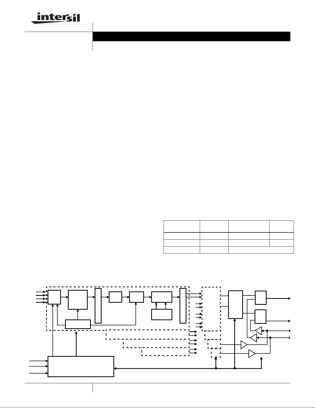
Block Diagram
SDA
SDB
SDC
SDD
P<15:0>
A<6:0>
{CNTRL}
I/Q
INPUT
DATA
SHAPING
FILTER/
FM MOD.
SAMPLE
PARALLEL HOST INTERFACE
I/Q
NCO
1
I/Q I/Q I/Q
HALF
BAND
GAIN PROFILE
INTPL
FILTER
CONFIGURATION AND CONTROL BUS
CAUTION: These devices are sensitive to electrostatic discharge; follow proper IC Handling Procedures.
1-888-INTERSIL or 1-888-468-3774
COMPLEX
MIXER
SIN COS
CARRIER
NCO
CHANNEL 0
CHANNEL 1
CHANNEL 2
CHANNEL 3
I/Q
GAIN CONTROL
| Intersil (and design) is a registered trademark of Intersil Americas Inc.
All other trademarks mentioned are the property of their respective owners.
I0
Q0
4 CH
I1
SUM
Q1
I2
Q2
Σ
I3
Q3
Σ
Σ
Σ
Σ
Copyright Intersil Americas Inc. 2003, 2005. All Rights Reserved
DELAY
SUM
1
2
3
4
CAS
SUM
CAS
SUM
IOUT(19:0)
QOUT(19:0)
QIN(19:0)
IIN(19:0)
Page 2
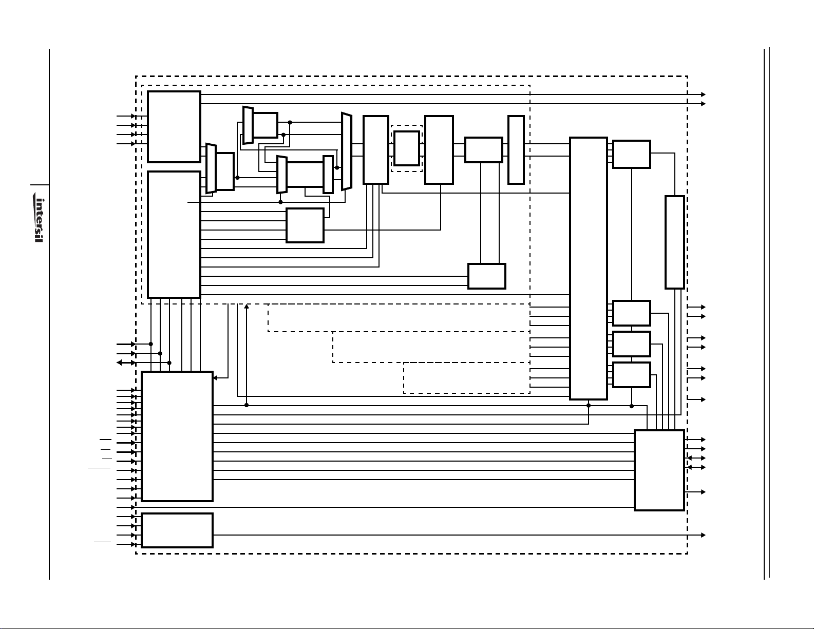
Functional Block Diagram
www.BDTIC.com/Intersil
ISL5217
SDA
SDB
SDC
SDD
2
CLK
A<6:0>
P<15:0>
TXENA
TXENB
TXENC
TXEND
UPDA
UPDB
UPDC
UPDD
WR
RD
CS
RESET
RDMODE
OUTEN<1:0>
TRITST
OFFBIN
TMS
TDI
July 8, 2005
FN6004.3
TCK
TRST
SERIAL
INTERFACE
I IN<15:0>
Q IN<15:0>
I IN<15:0>
Q IN<15:0>
SER._PAR.
CHANNEL
UP
INTERFACE
AND TIMING
<4:0>
UPDATE<3:0>
TX_ENABLE<3:0>
DEVICE
UPROCESSOR
INTERFACE
JTAG
16
I FM
Q FM
I SF
SHAPING
MUX
FILTER
SAMPLE
NCO
FM
MUX
MOD.
/
I FIFO
MUX
FIFO
1-7 DEEP
MOD. TYPE <1:0>
FID<31:0>
SR<47:0>
INTPL PHASES<1:0>
PHASE OFFSET<1:0>
GAIN<11:0>
GAIN PROFILE LENGTH<6:0>
OUTPUT_EN
CARRIER PHASE<15:0>
CARRIER FREQUENCY<31:0>
DUALQUADMODE (CH0 AND CH2 ONLY)
CH_SELECT<3:0>
ROUTEBUS_UPDATE
RESET
CASCADE_DELAY<1:0>
ROUTEBUS<15:0>
CASCADE_IN_ENABLE
OUTPUTMODE<1:0>
OUTPUTMODE2X
I_STROBE_EN
ISTROBEPOLARITY
TRITST_ENABLE_BUS<7:0>
/
16
Q FIFO
/
ISTROBEUPDATE
/
18
/
18
/
20
/
LIMITER
COARSE
PHASE<3:0>
20
20
MUX
/
/
HALF
BAND
GAIN PROFILE
BYPASS
CH_ENABLE<0>
FINE
PHASE<11:0>
INTERPOLATION
SCLKA
FSRA
21
/
COMPLEX
21
MIXER
/
FILTER
COS<18:0>
SIN<18:0>
CARRIER
NCO
CHANNEL 0
CHANNEL 1
CHANNEL 2
CHANNEL 3
GAIN CONTROL
I<21:0>
Q<21:0>
I<21:0>
Q<21:0>
CH_EN<1>
I<21:0>
Q<21:0>
CH_EN<2>
I<21:0>
Q<21:0>
CH_EN<3>
ROUTING
CONTROL
4 INPUT
SUMMER
1
4 INPUT
SUMMER
2
4 INPUT
SUMMER
3
4 INPUT
SUMMER
4
OUTPUT
CONTROL
PROGRAMMABLE DELAY
ISL5217
SCLKB
FSRB
SCLKC
FSRC
SCLKD
FSRD
ISTRB
IOUT<19:0>
QOUT<19:0>
IIN<19:0>
QIN<19:0>
SYNCO
TDO
Page 3
Pinout
www.BDTIC.com/Intersil
ISL5217
196 LdBGA
TOP VIEW
123456789 1110
A
IOUT14
B
IOUT15IOUT16 IOUT5
C
QOUT16
IOUT17IOUT18 P6
D
GND GND VCCIO VCCC VCCC VCCC
E
VCCCQOUT17 QOUT18
F
VCCC P1
QOUT19
G
CLK A4 A2QIN19
H
J
K
L
M
N
P
TCK GND RDQIN17 TMS
QIN15 UPDD
GND QIN14 UPDC VCCC
IIN14 TXENC SCLKB
IIN15 GND IIN7 IIN3
GND
QIN18
GND
QIN16 FSRB
QIN13
OUTEN1
OUTEN0
VCCC VCCC
TRST
TDO
QIN12
OFFBIN
QIN11
GND GNDIIN5 UPDB TXEND
VCCC GND
VCCIO I OUT0IOUT2IOUT4 P15 P12 P11IOUT13 IOUT12 IOUT10 GND IOUT8 IOUT6
IOUT1VCCIOIOUT3IOUT11 VCCIO GNDIOUT9
QOUT0QOUT3GND P14 P8QOUT15 QOUT12 QOUT9 IOUT7
QOUT1
QOUT4IOUT19 QOUT6 P4QOUT13 QOUT10
QOUT5QOUT7QOUT14 QOUT11 QOUT8 QOUT2
A6
A1
A0
SYNCO
QIN3QIN5QIN9 QIN7
FSRA
RDMODEQIN2IIN18 SCLKDQIN8 QIN6
SDB SDDQIN1IIN16 QIN4
QIN0IIN9 VCCC GND
GND P13 P10 P9
GND
FSRCIIN19 FSRDTDI
UPDA
VCCIOIIN1
SDAIIN0IIN13 IIN2 SDC TXENB SCLKAIIN12 IIN10 IIN8 IIN6 IIN4
P2 GNDRESET
P0ISTRB GND A5TRITST
CS
12
P7
A3
GNDVCCIOVCCCVCCIOVCCIO
TXENA
13 14
P3P5
WR
VCCC
GND
SCLKCIIN17 IIN11 QIN10
POWER PIN
GROUND PIN
SIGNAL PIN
THERMAL BALL
NC (NO CONNECTION)
NOTE:
Thermal balls should be connected to the ground plane.
3
FN6004.3
July 8, 2005
Page 4
ISL5217
www.BDTIC.com/Intersil
Pin Descriptions (all signals are active high unless otherwise stated)
NAME TYPE DESCRIPTION
POWER SUPPLY
VCCC - Positive Device Core Power Supply Voltag e, 2.5V ±0.125V.
VCCIO - Positive Device Input/Output Power Supply Voltage, 3.3V ±0.165V.
GND - Ground, 0V
MICROPROCESSOR INTERFACE AND CONTROL
CLK I Input Clock. All processing in the ISL5217 occurs on the rising edge of CLK.
RESET
P<15:0> I/O Data bus. Bit 15 is the MSB.
A<6:0> I Address bus. Bit 6 is the MSB.
CS
RDMODE I Read Mode. Read mode selects the Read/Write mode for the Microprocessor Interface. When low the device is
WR
RD
OFFBIN I Offset Binary. When set to 1, the output data bus format is offset binary. When set to 0 the output data bus format
OUTEN<1:0> I Output Three-state Control. OUTEN<1:0> is decoded to provide three-state control of the output data buses. When
TRITST I Tester Three-State Control. This signal determines how the OUTEN<1:0> is decoded to provide the necessary
SERIAL DATA / SYNCHRONIZATION AND FIFO STATUS
SDA, SDB,
SDC, SDD
SCLKA,
SCLKB,
SCLKC,
SCLKD
FSRA,
FSRB,
FSRC,
FSRD
I Reset. (Active Low). Asserting reset will clear all configuration registers to their default values, halting all processing.
I Chip Select. (active low). Enables device to respond to µP access. NOTE: See Appendix A, Errata Sheet.
configured for separate RD
and Data Strobe inputs. Internally pulled down.
I Write Strobe, (active low). Dual function input. The input is configured for Write Strobe when RDMODE is low. When
RDMODE is high the input is configured for Data Strobe.
Write Strobe. The data on P<15:0> is written to the destination selected by A<6:0> on the rising edge of WR
is asserted (low).
CS
Data Strobe. The data on P<15:0> is written to the destination selected by A<6:0> on the rising edge of Data strobe
when RD
RD
I Read Strobe (Active Low). Dual function input. The input is configured for Read Strobe when RDMODE is low.
When RDMODE is high the input is configured for Read/Write
Read Strobe. The data at the address selected by A(6:0) is placed on P<15:0> when RD
CS
Read/Write
is 2’s complement.
TRITST is asserted, the three-state control divides the 80-bit output into eight groups of 10-bits each. When TRITST
is deasserted, the three-state control operates on the 20-bit real and imaginary cascade out data buses.
three-state controls when in normal or tester applications. Set low for normal operation.
I Serial Data A-D. (SDX) Serial Data Input for the I and Q vectors. The processing channel selected for this data will
shift the data in on the rising edge of its serial TX clock. The data vectors are shifted in with the MSB first.
O SERIAL CLK A-D. (SCLKX
the serial data port. When symbol data is input through the µP port the output is SAMPLE CLK 0-3. The polarity of
SCLKX
Serial Clock. Programmable rate clock signal provided to the data source to shift serial data out. Programmed rates
can be CLK/(1-32), or 32x sample clock. See control word 0x17, bit 15 for shut-off conditioning.
SAMPLE CLK. Signal provided to the data source to indicate when data is being transferred from the FIFO to the
shaping filter. The SAMPLE CLK output is generated by the sample rate NCO and has approximately 50% duty
cycle. The sample is taken on the high-to-low transition.
O FRAME STROBE A-D. (FSRX
is FRAME STROBE when symbol data is input through the serial data port. When symbol data is input through the
µP port the output is FIFO READY 0-3. When control word 0x0c, bit 11 is set to one, the setting of the
FSRMode<1:0> bits in indirect address 0x407 determine the output. The polarity of FSRX
FRAME STROBE. Signal provided to the data source to initiate a serial word transfer. Alternatively selectable
through Se r ial Control 0x11, bit 1 4 to be Epoch frame strobe. Epoch is a pre-carry out of the fixed integer divider
instead of the serial frame strobe. The Epoch pre-carry out is six clocks ahead of the true carry out and can be used
to synchronize fixed integer dividers of other devices. See control word 0x17, bit 15 for shut-off conditioning.
FIFO READY. Indicates the I and Q FIFO pointer is less than the programmed FIFO depth.
UPDX
output. When 0x0c, bit 11 is set to one, and FSRMode<1:0> is set to 11, the internal channel TXENX
Table 43 for additional details.
is low and CS is asserted ( l o w ) or read from the address selected by A<6:0> placed on P<15:0> when
is high and CS is asserted (low).
is asserted (low).
Strobe. Determines the type of µP access.
is programmable.
or TXENX: When 0x0c, bit 11 is set to one, and FSRMode<1:0> is set to 10, the internal channel UPDX is
and WR strobe inputs. When high the device is configured for a common Read/Write
when
Strobe.
is asserted (low) and
) Dual function output. The output is SERIAL CLK when symbol data is input through
) Multiple Function Output. When control word 0x0c, bit 11 is set to zero, the output
is programmable.
is output. See
4
FN6004.3
July 8, 2005
Page 5
ISL5217
www.BDTIC.com/Intersil
Pin Descriptions (all signals are active high unless otherwise stated) (Continued)
NAME TYPE DESCRIPTION
TXENA,
TXENB,
TXENC,
TXEND
UPDA, UPDB,
UPDC, UPDD
SYNCO O Synchronization Output. The processing of multiple ISL5217 devices can be synchronized through software by
MODULATED DATA (80)
IOUT(19:0) O Output Data Bus A (19:0). Output bus A contains the digital modulated QUC output samples from Output
QOUT(19:0) O Output Data Bus B (19:0). The output bus contains the digital modulated QUC output samples from Output
IIN(19:0) I/O I Cascade In (19:0) or OUTPUT BUS C. Dual function I/O bus. The bus is configured for input when the output mode
QIN(19:0) I/O Q Cascade in (19:0) or Output Data Bus D. Dual function I/O bus. The bus is configured for input when the output
ISTRB O I data strobe. (active high). Used in the muxed I/Q mode. When asserted, the output data buses contain valid I data.
JTAG TEST ACCESS PORT
TMS I JTAG Test Mode Select. Internally pulled up.
TDI I JTAG Test Data In. Internally pulled up.
TCK I JTAG Tes t Clock.
TRST
TDO O JTAG Test Data Out.
I Transmit Enable A-D. (TXENX
(conditioned by control word 0x0c, bit 2), clear the data RAMs, and update the selected configuration registers upon
assertion. No additional requests for serial data will be made when TXENX
control word 0x0c, bit 3. The polarity of TXENX
with a programmable duty cycle. Two different programmable TXENX
between based on programmed cycle length. See control word 0x0c, bit 11 and Table 43 for additional details.
I Update A-D. (UPDX
the associated update mask bit is set. The polarity of UPDX
connecting the SYNCO of the master ISL5217 device to an UPDX
is programmable.
Summer/Formatter 1. The samples are updated on the rising edge of the CLK. Bit <19> is the MSB.
Summer/Formatter 2. The samples are updated on the rising edge of the CLK. Bit <19> is the MSB.
is cascade in. The bus is configured for output for all other output modes.
I Cascade In. Input bus allows multiple parts to be cascaded by routing the digital modulated signal I CAS OUT,
(Bus A), from one QUC into Output Summer/Formatter 1 of a second QUC. I CAS IN (19:0) is in 2’s complement
format and is sampled on the rising edge of CLK. Bit<19> is the MSB.
Output Data Bus C. The output bus contains the digital modulated QUC output samples from Output
Summer/Formatter 3. The samples are updated on the rising edge of the CLK. Bit <19> is the MSB.
mode is cascade in. The bus is configured for output for all other output modes.
Q Cascade in. Input bus allows multiple parts to be cascaded by routing the digital modulated signal Q CAS OUT,
(Bus B), from one QUC into Output Summer/Formatter 2 of a second QUC. Q CAS IN (19:0) is in 2’s complement
format and is sampled on the rising edge of CLK. Bit<19> is the MSB.
Output Data Bus D. The output bus contains the digital modulated QUC output samples from Output
Summer/Formatter 4. The samples are updated on the rising edge of the CLK. Bit <19> is the MSB.
I JTAG Test Reset (Active Low). Internally pulled-up. This pin should be driven by the JTAG logic to obtain a TAP
controller reset, or if JTAG is not utilized, this pin should be tied to ground for normal operation. As recommended
in the 1149.1 standard documentation the TRST
a known state within the TAP logic on the ISL5217. This avoids potential damage due to signal contention at the
circuit’s inputs and outputs.
) The processing channel selected for this input updates the selected configuration registers, if
) The processing channel selected for this enable will force a channel flush
is deasserted, unless conditioned by
is programmable. Optionally, TXENX can be internally generated
cycles can be programmed and toggled
is programmable.
pin of the ISL5217 slaves. The polarity of SYNCO
test pin should be made active soon after power-up to guarantee
5
FN6004.3
July 8, 2005
Page 6
ISL5217
www.BDTIC.com/Intersil
Functional Description
The ISL5217 Quad Programmable UpConverter (QPUC)
converts digital baseband data into modulated or frequency
translated digital samples. The QPUC can be configured to
create any quadrature amplitude shift-keyed (QASK) data
modulated signal, including QPSK, BPSK, and m-ary QAM.
The QPUC can also be configured to create both shaped
and unfiltered FM signals. A minimum of 16 bits of resolution
is maintained throughout the internal processing.
The QPUC is configured via the microprocessor data bus,
using the A<6:0> address bus, P<15:0> data bus, RD
and CS
control signals. Configuration data that is loaded via
, WR
this bus includes the individual channel’s 48-bit Sample Rate
NCO center frequency, the 32-bit Carrier NCO center
frequency, the device modulation format, gain control, input
mode control, reset control and sync control. The I and Q
baseband channels each have a 256 tap FIR filter whose
coefficients and configuration are also programmed via the
µP interface. Similarly, the control signals for the I and Q
channel interpolation filters are programmed via the µP
interface. Discussion in the following sections utilizes the
register definitions for channel 0. Channels 1-3 are similarly
configured in accordance with the Table 10 Memory Map.
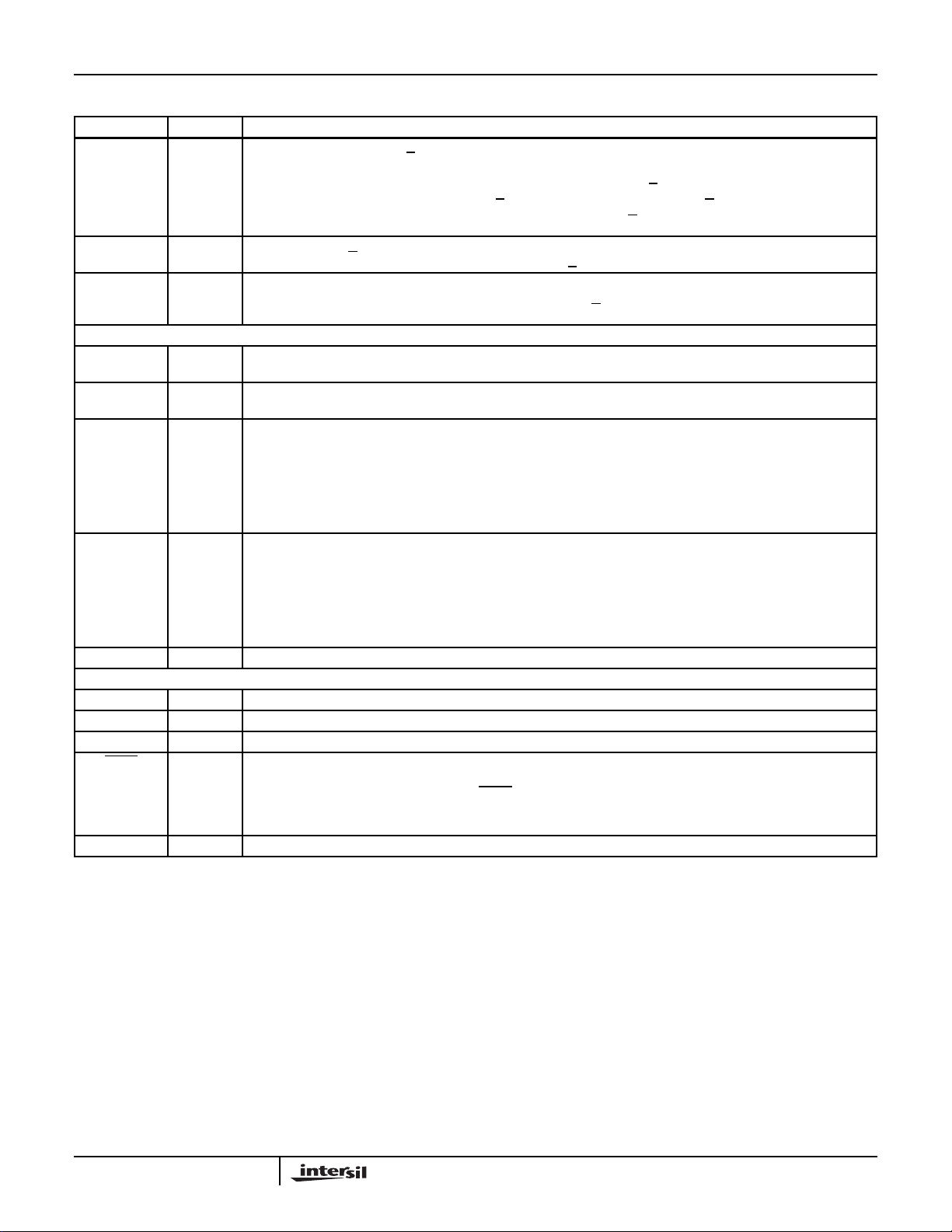
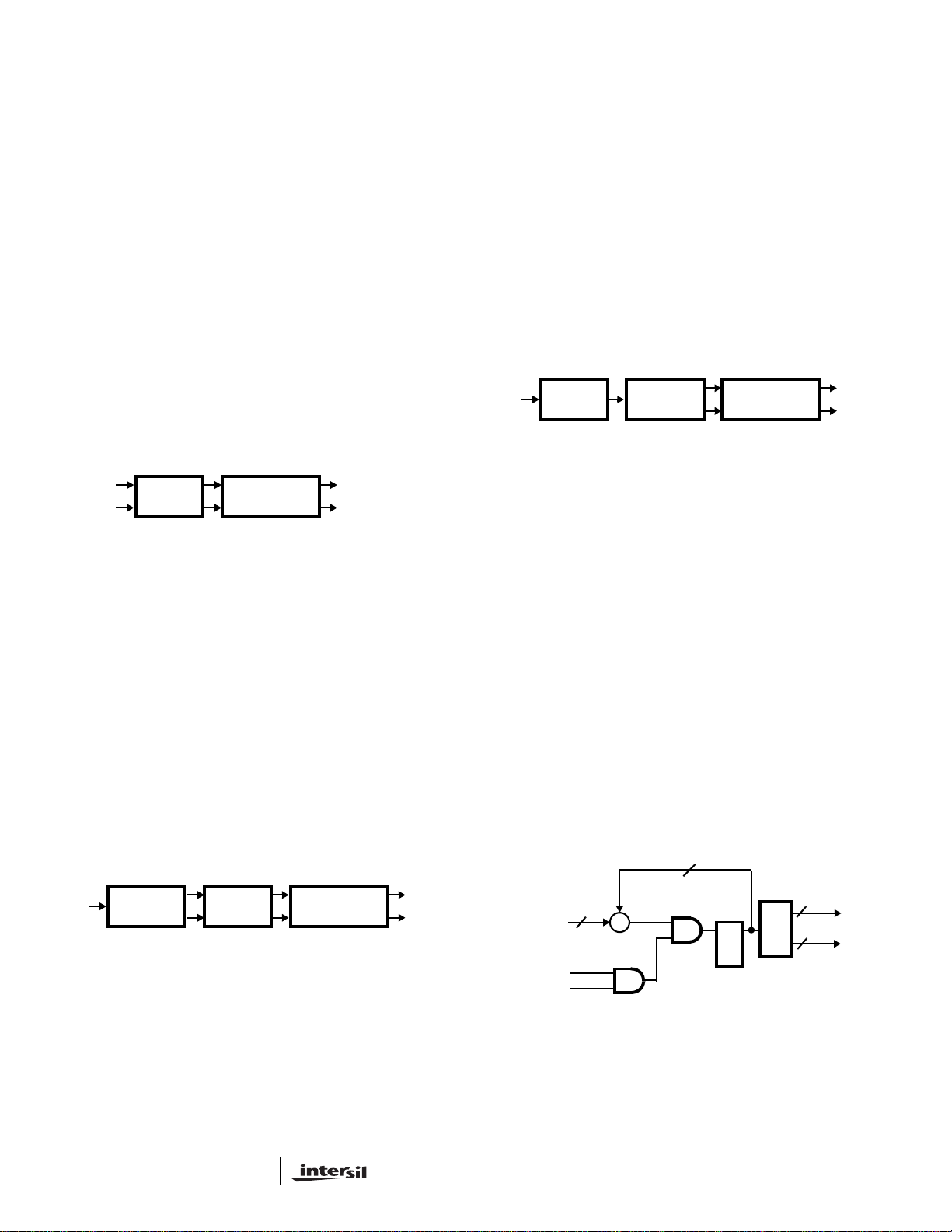
Data Input
The I/Q sample pairs can be input serially through 1 of 4
serial interfaces or in parallel through the µP addressable
registers as shown in Figure 1.
back 16-bit serial transfers can occur by setting control word
(0x17, bits 14:13) both high. The serial process begins with the
first serial clock after the start of a sample clock. The frame
strobe is asserted for one serial clock and starts the I and Q
time slot counters. The TXENX
pin or Main control (0X0c, bit 0)
S/W TX enable must be asserted to enable the frame strobe
out. Additional requests for serial data, with TXENX
deasserted, are controlled by bit 3 of control word 0x0c. The serial
interface may be programmed to be dependent or independent
of TXENX
control. The I and Q time slot counters, programmed
through 0x12, bits 9:0 and 0x13, bits 9:0, control the duration of
the serial to parallel conversion of the serial data input. The
counters are loaded to count the number of serial clocks from
the frame strobe to shift in the last data bit of that sample. The
time slot counters are 10-bits to allow multiple channels to
share a common serial data input. The MSB is always shifted
first, but the order of the I and Q serial data is flexible due to the
variability of the time slot counters. The received serial word is
MSB justified prior to loading into the FIFO holding register
based on the serial word length, programed through Serial
control (0x11, bits 3:2) to 4, 8, 12, or 16 bits.
Although each channel has control of a serial interface it may
select serial data from one of the other interfaces. Serial
control (0x11, bits 1:0) selects 1 of 4 serial data ports for the
channel. The serial data transfer format is shown in Figure 2.
SCLKX
UPDX
0x11, 3:2
SERIAL TO
0x0, 15:0
0x1, 15:0
PARALLEL
0x12, 9:0
0x13, 9:0
PARALLEL
0x11, 15
I sample (15:0)
2:1 MUX
Q sample (15:0)
2:1 MUX
0x11, 1:0
SDA
SDB
SDC
SDD
A<6:0>
P<15:0>
FIGURE 1. SINGLE CHANNEL DATA INPUT PATH
4:1 MUX
CHANNEL
µP INTERFACE
Serial
The serial mode allows the device to shift the I and Q samples
serially into the FIFO holding registers. The serial input format
is selected when Serial control (0x11, bit 15) is high. The serial
interface is three-wire interface controlled by the channel. The
serial clock and frame strobe are driven by the channel to clock
the serial data from the source into the serial data port. The
serial clock can operate at the clock rate, at a divided clock rate,
or be driven at 32x the sample clock rate. Serial control (0x11,
bits 13:8) configure the serial clock. In the 32x mode, back to
TXENX
FSRBX
SDX
INACTIVE
DON’T CARE
FIGURE 2. SERIAL DATA TRANSFER
Q<MSB>
Q<LSB>
I<MSB>
I<LSB>
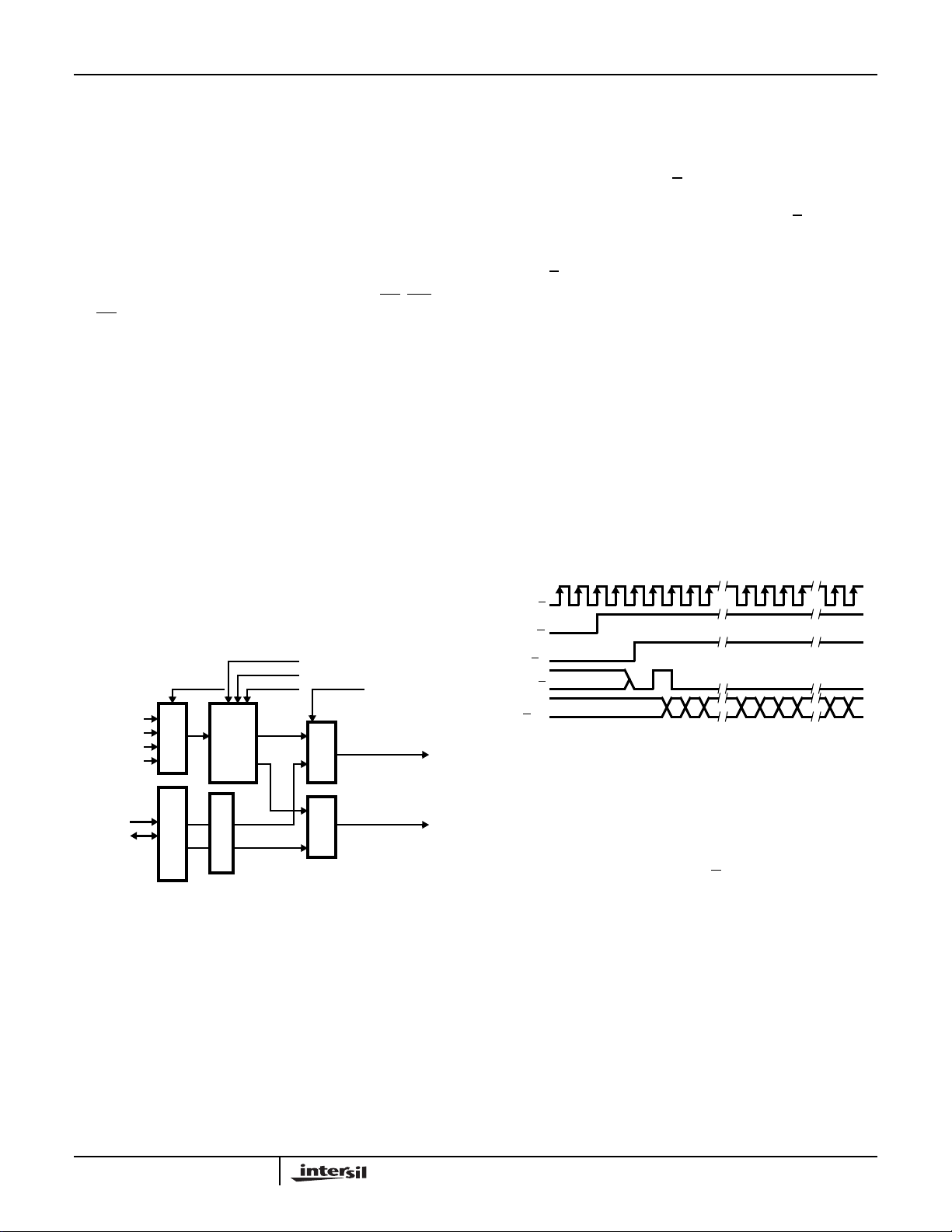
The ability to select the serial input source allows multiple
QPUCs to share a single microprocessor interface with their
processing synchronized through the master QPUC SYNCO
being tied to the slave device UPDX
. Conversely, multiple
6
FN6004.3
July 8, 2005
Page 7
ISL5217
www.BDTIC.com/Intersil
microprocessors can share a single QPUC as shown in
Figure 3.
ISL5217
QPUC
CHANNEL 0
CHANNEL 1
CHANNEL 2
CHANNEL 3
µP
SCLKX
FSRX
SDX
MASTER
ISL5217
QPUC
SLAVE
ISL5217
QPUC
SLAVE
ISL5217
QPUC
SLAVE
ISL5217
QPUC
FIGURE 3. MULTIPLE CONFIGURATIONS
UPDX
SYNCO
UPDX
UPDX
UPDX
µP
µP
µP
µP
SCLKX
FSRX
SDX
SCLKX
FSRX
SDX
SCLKX
FSRX
SDX
SCLKX
FSRX
SDX
Parallel
The parallel mode allows the µP to write the I and Q
samples directly to the FIFO holding registers. The parallel
input format is selected when Serial control (0x11, bit 15) is
low. The normal µP write order is the Q sample, Control
word 0x1, followed by the I sample, Control word 0x0.
Writing to Control word 0x0 generates the update strobe to
move the data from the FIFO holding register into the first
location of the I/Q FIFO. The first location of the I/Q FIFO is
available for read back. The µP can perform back-to-back
write accesses to Control words 0x1 and 0x0, but must
maintain four f
address. This limits the maximum µP write access rate for
an I/ Q sample pair to 104MHz/4 = 26MHz. The Read/Write
format for a parallel data transfer is shown in Figure 4
CLK
RDMODE
RD
periods between accesses to the same
CLK
The input source to the FIFO is selected by Serial control
(15). The FIFO pointer is incremented every time data is
written into the FIFO. The transferring of data into the FIFO
does not occur until both I and Q have been receiv ed when
the sample data is input in a serial fashion. When the
sample data is input in a parallel f ashion, the transferring of
data into the FIFO occurs when the µP writes to Control
Word 0 (I data).
While the input source determines the write rate, the
shaping filter determines the read rate. The maximum read
rate occurs when the shaping filter constraints for Data
Span (DS) and Interpolation Phases (IP) equal four. For a
clock rate of 104MHz, the maximum read rate is
determined by f
/(DS)(IP), which is 104MHz/16 =
CLK
6.5MHz. See the Shaping Filter Section for more details.
When the Shaping Filter requires another data sample, a
request is made to the FIFO for data and the FIFO pointer
is decremented. Figure 5 indicates the timing of a request
for data from the Shaping filter to the actual appearance of
data at the FIFO output. An “empty” FIFO detection causes
zero valued data to be entered into the shaping filter. The
FIFO can be forced to enter zero v al ued data by setting the
on-line mode to false. The on -line mode is enab led by Main
control (0xc, bit 6). A “full” FIFO detection prevents data
from being pushed out of the FIFO before the filter requests
it. Writing to a full FIFO is treated as an error condition that
will result in a soft reset of the channel to prevent
transmission of erroneous data over the air. The full FIFO
channel reset can be disabled by control word 0x0c, bit 1.
A programmable FIFO depth threshold sets when the
FIFORDY signal is asserted, alerting the data source that
more data is required. The FIFORDY signal assists the
data source in maintaining the desired FIFO data depth.
The data FIFO depth threshold for both I and Q inputs is set
by Main control (0xc, bits 10:8). The SAMPLE CLK may be
used instead of FIFORDY to indicate when data has been
transferred from the FIFO to the shaping filter. See the pin
description table for additional details and Figure 5 for the
input data latency.
WR
A<6:0>
P<15:0>
FIGURE 4. PARALLEL DATA TRANSFER
01
00 01 00
Q I Q I
01 00
Q I
FIFO
The FIFO provides the interface and data storage between
the input source and the shaping filter or FM modulator. The
FIFO can hold up to seven I /Q sample pairs. The block
diagram is shown in Figure 6.
7
FN6004.3
July 8, 2005
Page 8
Data Modulation Path
www.BDTIC.com/Intersil
Three data path options are provided, one for each
modulation format. The modulation format is selected using
FIR Control (0xd, 3:2). The modulation paths are defined in
the following subsections.
ISL5217
WR
CLK
DLY DATA
DFF 1
DFF 2
DFF 3
DFF 4
Write_FIFO
REG1
FIFORDY
FIFO NEEDS
MORE DATA
1234
FIGURE 5. FIFO DATA AND ENABLE TIMING
DFF1 DFF2 DFF3 DFF4
R
>
0X11, 3:2
0X12, 9:0
0X13, 9:0
SERIAL TO
PARALLEL
0X0, 15:0
0X1, 15:0
PARALLEL
E
G
A<6:0>
P<15:0>
SDA
SDB
SDC
SDD
A(000)
WR
0X11, 1:0
4:1 MUX
CHANNEL
ΜP INTERFACE
FIFO NEEDS
MORE DATA
CLOCK SYNCHRONIZATION
R
R
E
G
>
SERIAL_WRITE_TO_FIFO
0X11, 15
2:1 MUX
2:1 MUX
R
E
E
G
G
>
>
I SAMPLE (15:0)
Q SAMPLE (15:0)
0X11, 15
2:1 MUX
ZERO’S
A(2:0)
0XC, 10:8
ALMOST EMPTY
THRESHOLD
FM ENABLED
WRITE_FIFO
R
R
R
E
E
G
G
>
>
0 1
E
G
>
R
E
G
>
8:1 MUX
COMP
COMP
8:1 MUX
R
R
E
G
>
R
E
E
G
G
>
>
IFIFO(15:0)
FIFORDY
DFF
QFIFO(15:0)
R
R
E
E
G
G
>
>
† All Registers are clocked at CLK unless shown otherwise.
FIGURE 6. I AND Q FIFO BLOCK DIAGRAM
8
R
R
E
E
G
G
>
>
R
R
E
G
>
R
E
E
G
G
>
>
WRITE_FIFO
FN6004.3
July 8, 2005
Page 9
ISL5217
www.BDTIC.com/Intersil
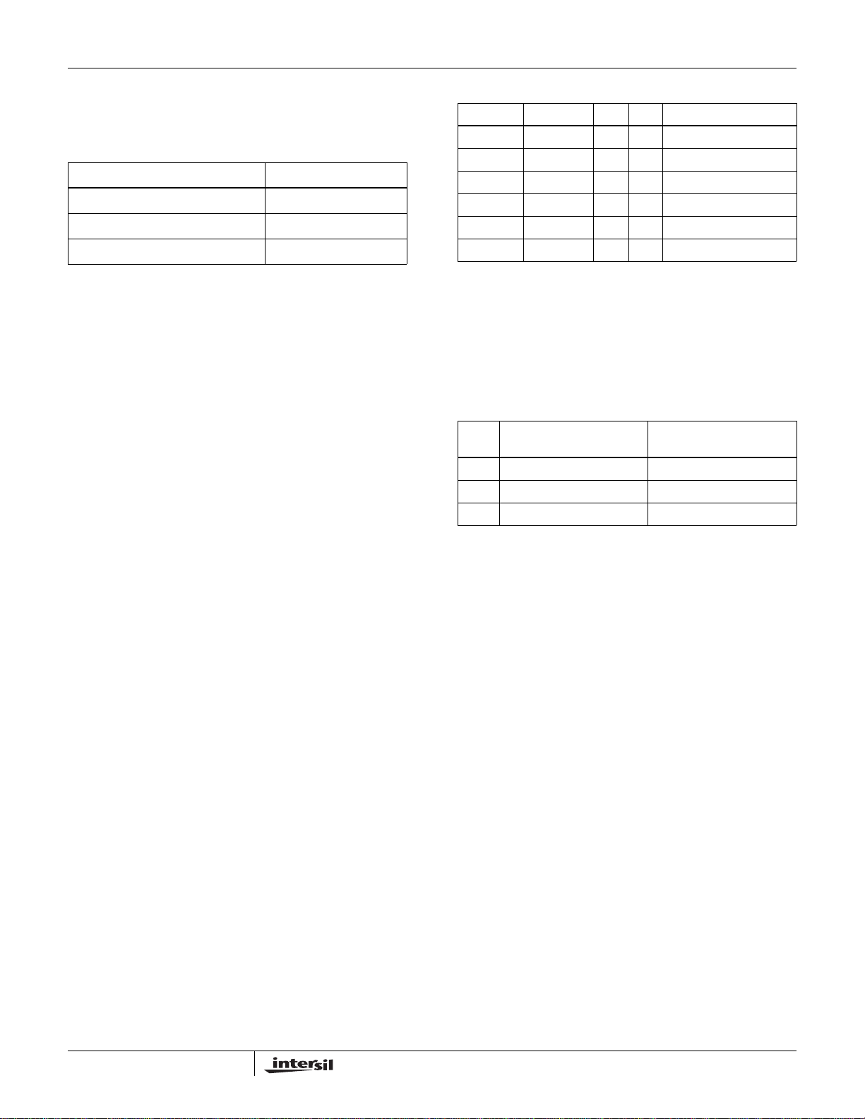
Modulation Mode 00 - QASK
This modulation mode configures the QPUC as a BPSK,
QPSK, OQPSK, MSK or m-QAM modulator. The block
diagram is shown in Figure 7. The data FIFO outputs are
routed to the shaping filters. Here the samples are
interpolated by 4, 8, or 16 and shaped using a FIR filter with
up to a 256 taps. The filter impulse response can span 4-16
input samples. A half (input) sample delay can be inserted in
the I/Q path after the FIR and is enabled through Main
Control (0xc, bit 13). Th e 20- bit output of the shaping filter is
routed through a gain adjust multiplier controlled by 0x0a,
bits 11:0 and into the interpolation filter. The interpolation
filter interpolates by a factor set in the resampling NCO with
the Interpolation Phases controlled by 0xd, bits 1:0. The
output of the interpolation filter is at the master clock
frequency , CLK. The samples are then mixed with the carrier
L.O. for quadrature upconversion. The output is then
summed with the cascade input signal, saturated (in the
case of overflow), and formatted for output.
I
SHAPING
Q
FILTER
FIGURE 7. QASK
GAIN
PROFILE
TO
HALFBAND
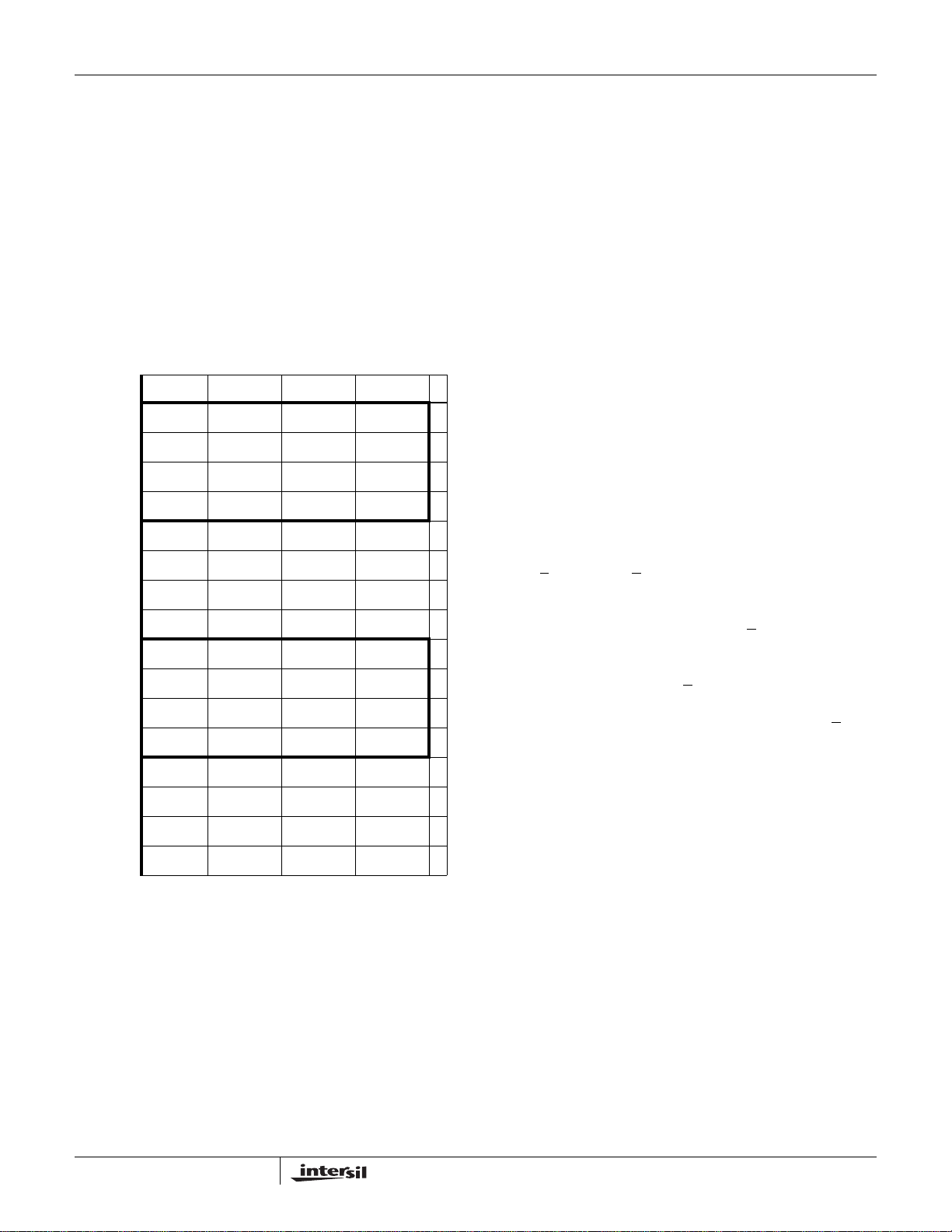
Modulation Mode 01 - FM with Bandlimiting Filter
This mode configures the QPUC as an FM modulator with
post-modulation filtering. The block diagram is shown in
Figure 8. This mode provides for FSK and FM modulation
schemes. In this mode, the I input samples drive the
frequency control section of a quadrature NCO to produce a
zero IF FM signal. The 16-bit FM quadrature signals are then
routed to the shaping FIR filter and into the interpolation filter
for bandlimiting and interpolation up to the master clock rate.
The quadrature filtered FM signals are then upconverted to
the carrier frequency by the carrier NCO and mixers. The
output is then summed with the cascade input signal,
saturated (in the case of overflow), and f o rmatted for output.
Note that pulse shaping in this mode must be provided prior
to the QPUC.
modulated quadrature samples are then up sampled in the
interpolation filter to the output sample rate. The baseband
modulated signal is then upconverted to the carrier
frequency by the carrier NCO and mixers. The output is then
summed with the cascade input signal, saturated, and
formatted for output.
In Mode 10, the amplitude out of the shaping filter needs to
be limited in order to prevent frequency excursions that
cannot be filtered out in the interpolation filter.
NOTE: THE QUALITY OF THE FM SIGNAL IS AFFECTED BY
THE AMPLITUDE SLEW RATE OUT OF THE SHAPING FILTER.
AS A RULE OF THUMB, LIMITING THIS SLEW RATE TO LESS
THAN 1/8 THE SAMPLE RATE WILL MINIMIZE THIS
DISTORTION.
SHAPING
I
FILTER
FIGURE 9. FM WITH PULSE SHAPING
FM
MODULATOR
GAIN
PROFILE
TO
FM Modulator
The FM modulator provides for frequency modulation of the
carrier center frequency by the QPUC input data. The FM
modulator is driven either directly by the QPUC I input (Mode
01) or by the output of the FIR shaping filter (Mode 10). The
input data to the FM Modulator, is defined as dφ(n)/dt, where
φ(nT) is the phase of a theoretical sinusoid described by:
sn() A (cos φ nT()]+ j sin φ nT()[]); A ≈ 1 in Modulator[=
The block diagram is shown in Figure 10. The input to the
FM modulator, dφ(n)/dt, is integrated via the NCO
accumulator. The NCO accumulator output represents
phase and is used to address a SIN/COS generator,
synthesizing a sinusoid of the form described in
Equation 1. The phase accumulator feedbac k of the NCO is
20 bits and 18 bits of the phase word are routed to the
SIN/COS generator. Eighteen bits of amplitude are
provided on the Sine and Cosine outputs.
20
(EQ. 1)
HALF BAND
I
FM
MODULATOR
FIGURE 8. FM WITH BANDLIMITING
SHAPING
FILTER
Modulation Mode 10 - FM with Pulse Shaping
GAIN
PROFILE
TO
HALF BAND
dφ(nT)/dt
01 OR 10
16 or 20
FM
MODE
FIGURE 10. FM MODULATOR BLOCK DIAGRAM
This mode configures the QPUC as a FM modulator with
pre-modulation baseband pulse shaping. The block diagram
is shown in Figure 9. The data from the FIFO (I channel only)
is routed to the FIR shaping filter. The FIR shaping filter
output drives the frequency control section of a quadrature
NCO to produce a zero IF FM signal. These 18-bit FM
The transfer function of the FM modulator is de fined by the
change in degrees per sample value, dφ(nT)/dt, where
dφ(nT)/dt is a 16-bit, twos complement, fractionally notated
frequency control word with a range from -F
+F
SAMP
/2. F
SAMP
9
φ(nT)
∑
R
E
G
>
ROM
SIN/COS
SAMP
COS[φ(nT)]
18
SIN[φ(nT)]
18
/2 to
is defined as the sample rate into the FM
FN6004.3
July 8, 2005
Page 10
ISL5217
www.BDTIC.com/Intersil
modulator. The maximum phase step that can occur in one
clock is ±180 degrees. Tab le 1 pro v ides the change in phase
weighting of the input bits.
TABLE 1. PHASE WEIGHTING
dφ(nT)/dt DEGREES/SAMPLE
1000 0000 0000 0000 -180
0000 0000 0000 0000 0
0111 1111 1111 1111 ~+180
Shaping Filter
The shaping filter provides the necessary pulse shaping
required on the input data to implement various QASK and
shaped FM modulation formats. Two identical shaping filters
(one each for the I and Q paths) are provided. The shaping
filter architecture uses a NCO controlled interpol ating FIR,
capable of 4, 8, or 16 interpolation phases. The number of
interpolation phases, (IP) is loaded into FIR Control (0xd,
bits 1:0). The span of the impulse response of the polyphase
filter can vary from 4-16 data samples. The desired sample
Data Span, (DS) value minus one is loaded into FIR Control
(0xd, bits 7:4). Thus, the required number of coefficients (or
filter span) becomes:
# Coefficients = (DS)(IP)
The Interpolation Phase also determines the rate to compute
a polyphase output by selecting the appropriate timing from
the Sample Rate NCO to drive the shaping filter at 4x, 8x, or
16x the input sample rate. The Data Span selects the
number of samples to convolve. Each convolution requires
DS reference clocks for each phase of the filter. An output is
calculated (IP) times for each input sample. To allow
sufficient processing time for each output, the reference
clock must be as follows:
CLK DS()IP()f
()≥
S
Conversely, the input sample rate requires:
f
SfCLK
where f
[IP()⁄ DS()]≤
is the frequency of the reference clock, IP is the
CLK
shaping filter interpolate rate; and DS is the number of data
samples in the filter span. For example, if f
CLK
the filter span is 16 samples, and the interpolation rate is 16,
then the maximum input sample rate, f
is 104/256 =
S
406.25kHz. Table 2 shows several examples of calculations
for FIR input sample rates based on master reference clock
rate, number of data samples, and interpolation rate. The
data exits the shaping filters at the interpolated rate.
(EQ. 2)
(EQ. 3)
(EQ. 4)
= 104MHz,
TABLE 2. EXAMPLE CALCULATIONS
EXAMPLE f
1 104MHz 16 16 104/256 = 406.25kHz
2 104MHz 16 8 104/128 = 812.5kHz
3 104MHz 16 4 104/64 = 1.625MHz
4 104MHz 10 4 104/40 = 2.600MHz
5 104MHz 8 4 104/32 = 3.250MHz
6 104MHz 4 4 104/16 = 6.500MHz
CLK
DS IP MAX f
S
The shaping filters have programmable coefficients which
must be loaded via the microprocessor interface. The QPUC
supports loading coefficients for two shaping filters, with FIR
Control (0xd, bit 8) selecting the active filter. The I and Q
shaping filters are identical and may be loaded
simultaneously or separately , allowing f or different gains and
responses through the filter if desired.
TABLE 3. FIR CONTROLS
IP
16 0 128
STARTING ADDRESS
W/FIR CONTROL (8) = ‘0’
40 8
80 8
STARTING ADDRESS
W/FIR CONTROL (8) = ‘1’
Because 16 interpolation phases are possible, the
coefficients are structured in sets of 16, one set for each
phase of the shaping filter. The convolution algorithm
sequentially steps through each of these phases, beginning
with phase 0. The coefficients for the shaping filters are
generated by designing the prototype filter at the
interpolated rate. The coefficients are then divided into
interpolation phases by taking every n
th
tap of the prototype
filter and storing the coefficient as an element of a coefficient
set. The IP value determines the addressing interval through
the prototype filter to create the coefficient sets for the filter
phases. The first coefficient set begins at address 0. The
next coefficient set begins at address 1 and continues in a
like manner for the remaining coefficient sets. For a 16 tap,
interpolate-by-4 filter, the calculations for filter 1 are:
Polyphase output 0 = (C0*D[n]) + (C4*D[n-1]) + (C8*D[n-2])
+ (C12*D[n-3])
Polyphase output 1 = (C1*D[n]) + (C5*D[n-1]) + (C9*D[n-2])
+ (C13*D[n-3])
Polyphase output 2 = (C2*D[n]) + (C6*D[n-1]) + (C10*D[n-2])
+ (C14*D[n-3])
Polyphase output 3 = (C3*D[n]) + (C7*D[n-1]) + (C11*D[n-2])
+ (C15*D[n-3])
If FIR Control (8) is set the calculations for filter 2 are:
Polyphase output 0 = (D0*D[n]) + (D4*D[n-1]) + (D8*D[n-2])
+ (D12*D[n-3])
10
FN6004.3
July 8, 2005
Page 11
ISL5217
www.BDTIC.com/Intersil
Polyphase output 1 = (D1*D[n]) + (D5*D[n-1]) + (D9*D[n-2])
+ (D13*D[n-3])
Polyphase output 2 = (D2*D[n]) + (D6*D[n-1]) + (D10*D[n-2])
+ (D14*D[n-3])
Polyphase output 3 = (D3*D[n]) + (D7*D[n-1]) + (D11*D[n-2])
+ (D15*D[n-3])
Table 4 details the coefficient address allocation for the
previous example. The interpolation phase is on the left and
the data span is across the top. The coefficient RAM address
followed by the coefficient term is listed in the table’s cell.
Table 49 details the coefficient address locations through
255.
TABLE 4. ADDRESS ALLOCATION
DS [n] DS [n-1] DS [n-2] DS [n-3]
IP0
IP1
IP2
IP3
IP4
IP5
IP6
IP7
IP8
IP9
IP10
IP11
IP12
IP13
IP14
IP15
0 CO 16C4 32C8 48C12 •
1 C1 17C5 33C9 49C13 •
2 C2 18C6 34C10 50C14 •
3 C3 19C7 35C11 51C15 •
4203652•
5213753•
6223854•
7233955•
8 D0 24D4 40D8 56D12 •
9 D1 25D5 41D9 57D13 •
10 D2 26 D6 42 D10 58 D14 •
11 D3 27 D7 43 D11 59 D15 •
12 28 44 60 •
13 29 45 61 •
14 30 46 62 •
15 31 47 63 •
The gain through the filter is:
A = (sum of coefficients) / interpolation rate.
The shaping filter contains saturation logic in the event that
the final output peaks over +/- 1.0. When using quadrature
modulation, saturation/overflow can occur when the input
values for I and Q exceed 0.707 peak. The shaping filter
coefficients may need to be reduced from full scale to
prevent saturation.
Gain Profile
The overall channel gain is controlled by both a gain profile
stage and a gain control stage, which provide identical scaling
for the I and Q upconverted data. The gain profile stage allows
transmit ramp-up and quench fading, to control the sidelobe
profile in burst mode. This is implemented through user control
of the rise and fall transitions utilizing a gain profile memory.
The gain profile memory is a 128 x 12 bit RAM which is loaded
with the desired scaling coefficients via indirect addressing of
memory spaces 0x000-0x07f. The pulse shaping is
implemented by linearly multiplying the programmed coefficient
by the shaping filter outputs at the f
The gain profile is enabled by FIR control (0xd, bit 15), with the
RAM address pointer being reset to zero on assertion of the
gain profile enable. Control of the pulse shaping is based on
TXENX
, as the TXENX rising edge causes the RAM pointer to
begin stepping through the profile until the RAM pointer
matches the Gain profile length programed into control word
(0x0b, bits 6:0). The falling edge of TXENX
process and the RAM pointer begins decrementing until it
reaches zero. The gain process is symmetric with respect to the
rising or falling edges of TXENX
profile block is set by control word (0x0b, bits 8:7) where bit 8
bypasses all latency alignment circuitry and uses TXENX
input to the channel. Setting control word (0x0b, bit 7) remov es
two edge latencies from the delay path and should be
combined with selection of DS = 3, IP = 4 in order to have
perfect symmetry through the gain profile block. The memory
coefficients may be loaded without taking the channel off-line.
This is implemented by setting the gain profile hold bit in control
word (0x0c, bit 14) which holds the last gain value and provides
access to the memory.
*IP, or coarse phase rate.
S
reverses the
. The latency through the gain
as
The loading options are programmable including read back
modes and are discussed in detail in the ‘Microprocessor
Interface’ section. Both 16-bit 2’s complement and 24-bit
floating point format are allowed. The 2’s complement
coefficient format of valid digital values ranges from 0x8001
to 0x7FFF. The value 8000 is not allowed. The 24-bit floating
point (20-bit mantissa with 4-bit exponent) mode allows an
exponent range from 0 to 15. An exponent of 0 indicates
multiplication of the coefficient by 2
-1
2
, down to a value of 15 being 2
complement, with 24-bit floating point mode enabled by
setting control word (0x17, bit 12).
0
, and an exponent of 1 is
-15
. The default mode is 2’s
11
The gain profile coefficients are programmed as unsigned
values:
Bit weight 2
Maximum 0x800 = 1.0
0x001 = 2
Minimum 0x000 = 0.0
0.2-1 2-2
... 2
-11
-11
FN6004.3
July 8, 2005
Page 12
ISL5217
www.BDTIC.com/Intersil
Gain Control
The gain control is implemented through a scaling multiplier
followed by a scaling shift. The combination of the multiplier
and shifter provide the final output gain of the channel. Gain
adjustmen t can vary from -0.0026 to -144 dBFS.
Given a desired attenuation, the scaling multiplier value,
Gain
Gain
where INT[X] is the integer part of the real number X.
Table 5 details a few scaling multiplier values and their
associated attenuations.
Given a desired attenuation, the shifting value Gain
(2:0) can be determined by a table look-up. Refer to Table 6.
GAIN
The gain control is loaded into Control Word 0xa.
0xa, bits 14:12 = Gain
0xa, bits 11:0 = Gain
(11:0) can be calculated by the following equati o n.
MULT
(11:0) = INT [10
MULT
TABLE 5. SCALING GAIN ATTENUATION
GAIN
MULT
(0xa, 11:0) GAIN (dBFS)
1111 1111 1111 -0.0026 99.97
1000 0000 0000 -6.021 50.0
0100 0000 0000 -12.041 25.0
0010 0000 0000 -18.062 12.5
0001 0000 0000 -24.082 6.25
0000 1000 0000 -30.103 3.125
0000 0100 0000 -36.124 1.5625
0000 0010 0000 -42.144 0.78125
0000 0001 0000 -48.165 0.39062
0000 0000 1000 -54.186 0.19531
0000 0000 0100 -60.205 0.097656
0000 0000 0010 -66.226 0.04828
0000 0000 0001 -72.247 0.02441
TABLE 6. GAIN SHIFT VALUES
SHIFT
(2:0) GAIN (dBFS)
000 -72.247 4096 0.02441
001 -48.165 256 0.39062
010 -30.103 32 3.125
011 -24.082 16 6.25
100 -18.062 8 12.5
101 -12.041 4 25.0
110 -6.021 2 50.0
111 0 1 100.0
|(Gain(db)| / 20 )212
SCALE BYSCALING GAIN
(2:0)
SHIFT
(11:0)
MULT
]
SCALING GAIN
(V
OUT/VIN
SHIFT
(V
OUT/VIN
)%
)%
Sampling NCO
The Sample Rate NCO provides the SAMPLE CLK and
sample clock phase information to the data input FIFO’s,
the shaping filters and the interpolation filters. The input
sample rate is set by the sample cloc k. The sample cl ock is
the MSB of the NCO accumulator and controls the
movement of sample data from the user to the shaping
filters. The coarse phase of the NCO accumulator controls
the processing of the shaping filter at 4x, 8x, or 16x the
sample clock rate. The fine phase of the NCO accumulator
controls the processing of the interpolation filter as it resamples the data from the shaping filter to the clock rate.
The block diagram is shown in Figure 11.
The sample frequency, SF, is set with 48-bit resolution. The
LSB is f
bits. Given a desired sample frequency, f
SF(47:0) can be calculated by the following equation.
SF (47:0) = INT [(f
The sample frequency, SF(47:0) is loaded 16 bits at a time
into Control Words 4, 5, and 6.
0x4, bits 15:0 = SF (47:32)
0x5, bits 15:0 = SF (31:16)
0x6, bits 15:0 = SF (15:0)
The output of the phase accumulator can be offset by phase
increments of 90 degrees without affecting the operation of
the phase accumulator. The desired offset increment is
loaded into FIR Control (0xd, bits 11:10).
Since it is not possible to represent all frequencies exactly
with an NCO, the phase accumulator length has been
extended to minimize the effect of phase error accumulation.
At an update rate of 1MHz, half an LSB of error in loading
the 48-bit accumulator is 1.8e-9. The accumulated phase
error after 1 year is 0.056 of a bit.
Leap Counter
In addition to lengthening the NCO accumulator, a 32-bit
counter is available for realizing fixed integer interpolation
rates. The carry-out of the fixed integer counter can be used
to clear the coarse and/or fine phase of the sample rate
NCO. The fixed integer counter also provides a precarry-out
that can be used to synchronize fixed integer counters in
other devices. The fixed integer counter is enabled by FIR
Control (0xd, bit 12).
In programming the FID to clear the NCO accumulator ,
consideration must be provided to ensure that FID is
programmed to clear the Error term only when the desired
error term should have been zero with an integer multiple of
the symbol rate. Selecting GSM as an example, the FID
should clear the NCO accumulator every third multiple of the
symbol rate or every 270833.333 * 3 sample clocks, as the
error term should only be zeroed during integer multiples of
/248. The internal accumulator resolution is 48
CLK
) * 2
48
]
/ f
s
CLK
the value f or
s,
12
FN6004.3
July 8, 2005
Page 13
ISL5217
www.BDTIC.com/Intersil
the symbol rate. This would clear the NCO accumulator
every 3 seconds or at a 1/3 Hz rate. The frequency of the
FID carryout can range from Fclk to Fclk/2^32. The value of
FID is determined from:
FID (31:0) = [(fclk / fco)]
Where fco is the desired frequency of the carryout, which in
the previous example is 1/3 Hz and the fclk is and integer
multiple of the sample frequency, say 65MHz. The resultant
value for the FID would be (65MHz/1/3Hz) or 195e6. The
programmed integer values for the FID are loaded 16 bits at
a time into Control Words 2 and 3.
0x2, bits 15:0 = FID (31:16)
0x3, bits 15:0 = FID (15:0)
Loading 195e6 into the FID would result in 0x2, being
0x0b9f, and 0x3 being 0x76c0.
SAMPLE FREQUENCY
ZERO
SYNCSEL
SYNCIN
MUX
WR CW3
WR CW21
RST
IP(1:0)
0 1
START
EDGE
GEN
R
E
G
>
R
E
G
>
RESET
EDGE
GEN
† ALL REGISTERS ARE
CLOCKED AT CLK
FIGURE 11. RE-SAMPLING NCO BLOCK DIAGRAM
2
EN
>
REG
SHIFTER
>
46
REG <
∑
REG
12
4, 3, OR 2
ACC
EnNCO
(CARRIER NCO)
48
SAMPCK
(MSB)
FINE
PHASE
COARSE
PHASE
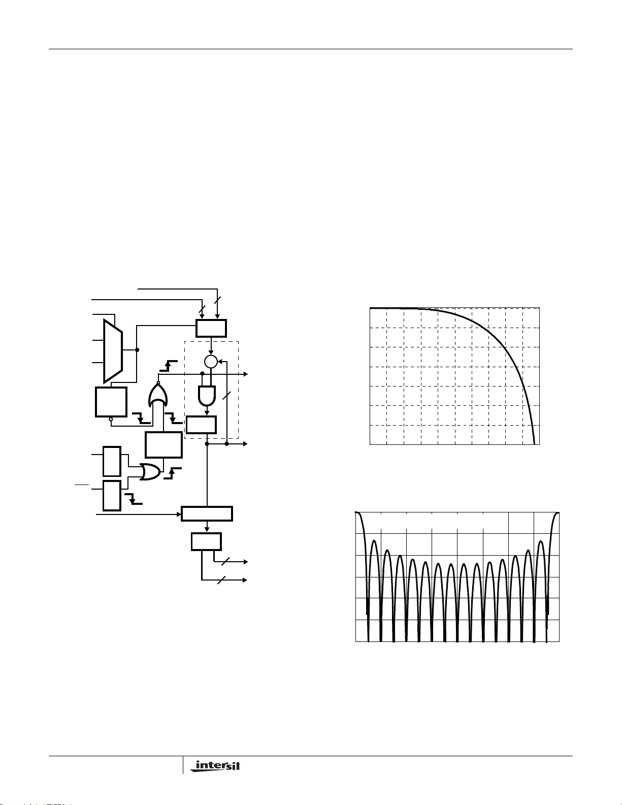
The output of this filter is rounded to 20-bits. The output is
checked for saturation and limited if necessary. The data
exits the halfband filter as a parallel I<20:0> and Q<20:0>
data stream at the rate of fs*IP*2. Figure 12 shows the
frequency response of the Half-Band filter.
Interpolation Filter
The shaped sample data is input to the interpolating filter at
the interpolation rate. The Interpolator filter resamples the
shaped I and Q data to establish the final output sample rate
of the channel. The output sample rate is always the clock
rate. The Interpolator uses the fine phase values from the
Symbol Rate NCO to compute the fine interpolated samples
at the clock rate. The number of interpolated samples is set
by the following ratio: n
The nulls in the interpolation filter frequency response align
with the interpolation images of the shaping filter. The
impulse response of the Interpolation filter is shown in
Figures 13A through 13C for varying interpolation ratios.
0
-20
-40
-60
-80
MAGNITUDE (dB)
-100
-120
-140
0 0.1 0.2 0.3 0.4 0. 5 0.6 0.7 0.8 0. 9 1
NORMALIZED FREQUENCY (NYQUIST=1)
FIGURE 12. HALF BAND FILTER RESPONSE
0
INTERPOLATION FILTER RESPONSE
-20
-40
-60
MAGNITUDE (dB)
-80
= f
CLK
/ f S / IP.
IS
Fixed Coefficient 11-TAP Interpolating
-100
Half-band
Following the post-FIR gain profile block is a fixed coefficient
11-tap interpolate by 2 Half-Band filter. The default mode is
to bypass the filter with the setting of control word 0x0d, bit 9
enabling the filter. If bypassed, the data to the filter is zeroed
which reduces power consumption. The halfband filter
coefficients are:
3, 0, -25, 0, 150, 256, 150, 0, -25, 0, 3
13
-120
FIGURE 13A. INTERPOLA TION FIL TER IMPULSE RESPONSE
512 1024 1536 2048 2560 3072 3584 4096
SAMPLE TIMES
L = 16; FOUT = 4096
FN6004.3
July 8, 2005
Page 14

ISL5217
www.BDTIC.com/Intersil
0
-20
-40
-60
-80
MAGNITUDE (dB)
-100
-120
FIGURE 13B. INTERPOLA TION FILTER IMPULSE RESPONSE
-0.05
-0.1
-0.15
-0.2
-0.25
-0.3
-0.35
-0.4
-0.45
MAGNITUDE (dB)
-0.5
-0.55
-0.6
-0.65
-0.7
FIGURE 13C. INTERPOLA TION FILTER IMPULSE RESPONSE
64 128 192 256
L = 16; FOUT = 4096
0
INTERPOLATION FILTER RESPONSE
8 16243240485664
L = 16; FOUT = 4096
INTERPOLATION FILTER RESPONSE
320 384 448 512
SAMPLE TIMES
SAMPLE TIMES
Carrier NCO
Following the interpolating filter section, the samples are
modulated onto a carrier signal via a complex multiply
operation. The Carrier NCO provides the quadrature local
oscillator references to the complex mixer.
The NCO has provisions for programming the frequency and
phase offset. The NCO has a 32 bit frequency control
providing sub-hertz resolution at the maximum clock rate.
The carrier NCO phase accumulator feedback can be preset
to synchronize multiple channels. The carrier NCO has a
32-bit 2’s complement programmable frequency increment
value which can range from -2
range of -f
CLK
/2 to ~f
CLK
frequency will range from -52MHz to +52MHz.
The maximum error is 104MHz/(2
carrier frequency can be calculated from the value loaded
into Control Address 0x8 and 0x9 by:
F
CARRIER
CR 31:0()f
31
to ~231 for a NCO output
/2. For f
CLK
= 104MHz, the
CLK
32
) = 0.0242Hz. The
32–
2
××=
(EQ. 5)
where CR(31:0) is the 32-bit frequency control word which
CLK
31
to ~231 for a NCO output range of
/2. f
is the CLK frequency.
CLK
can range from -2
-f
/2 to ~f
CLK
This NCO frequency range allows for spectral inversion.
Given a desired carrier frequency, the value for CR(31:0)
loaded into the part can be calculated by:
CR 31:0()INT F
⁄ *232][=
CfCLK
(EQ. 6)
where INT[X] is the integer part of the real number X.
The vector rotation can also be controlled by the sign of the
CF value. When CF is a positive value a counterclockwise
vector rotation is produced. When CF is a negative value a
clockwise vector rotation is produced.
The carrier frequency is loaded 16 bits at a time into Control
Words 8 and 9.
0x8, bits 15:0 = CF (31:16)
0x9, bits 15:0 = CF (15:0)
The 16-bit carrier phase offset initializes the most-significant
16-bits of the phase accumulator. The least significant 16
bits of the phase accumulator are cleared. Given a desired
carrier phase offset, the value CO(31:0) can be calculated by
the following equation.
CO 31:0()INT
PhaseOffset()°
---------------------------------------------
360°
*2
32
]=
(EQ. 7)
The carrier phase offset is loaded into Control Word 0x7.
Control Word 7 (15:0) = CO (31:16).
Complex Mixer
The complex mixer m ultiplies the sin/cos terms generated by
the carrier NCO sin/cos generator with the I and Q
interpolated sample data. The mixers can be bypassed by
programming the carrier frequency to zero. This action sets
the sin/cos terms generated by the carrier NCO to 0 and 1
respectively. The block diagram of the Car rier NCO/Comple x
Mixer is shown in Figure 14.
I(20:0)
+
∑
-
+
∑
+
Re (20:0)
Im (20:0)
SIN
SIN
19
19
19
19
COS
Q(20:0)
EN OUT
Q(20:0)
COS
I(20:0)
EN OUT
FIGURE 14. VECTOR MODULATOR/MIXER BLOCK DIAGRAM
14
FN6004.3
July 8, 2005
Page 15

ISL5217
www.BDTIC.com/Intersil
The resulting complex output is given by the following
equations.
Re mixer (20:0) = I(20:0) * cos(18:0) - Q(20:0) * sin(18:0)
Im mixer (20:0) = Q(20:0) * cos(18:0) + I(20:0) * sin(18:0)
(Vector weighting for block diagram)
1
I (20:0) = 2
Q (20:0) = 21... 2
sin (18:0) = 20... 2
cos (18:0) = 20... 2
Re mixer(20:0) = 21... 2
Im mixer(20:0) = 21 ... 2
.. 2
-19
-19
-18
-18
-19
-19
Output Processing
Output processing sums the modulated output of each
channel to provide multi-carrier outputs. There are four
4-channel summers, which combined with the outputs IOUT,
QOUT, and bidire ctional outputs IIN and QIN can be
configured by the user to support eight output modes. The
output mode is determined by Device Control 0x78 bits 9:8
and Main Control 0xc, bit 7.
Output Modes
Cascade Mode: In this mode IIN<19:0> and QIN<19:0> are
configured as inputs for the real and imaginary cascade
inputs. This is the only mode where IIN and QIN are
configured as inputs.
The cascade input allows for more than four multi-channel
transmissions by summing the complex modulated signals
from other device’s with the four channel summer . A cascade
chain of four devices allows up to sixteen carriers. Each
device delays it’s 4-channel summation to align with the
cascade in from the previous device. Device Control 0x78
bits 2:1, Cascade delay <1:0>, identifies the position in the
cascade chain to select the appropriate delay. Device
Control 0x78, bit 3, Cascade input enable, zeroes the
cascade-in data when the port is not in use. The output of
the summation is saturated to prevent roll-over.
Real: Real data is output on IIN, QIN, IOUT, and QOUT.
Imag: Imaginary data is output on IIN, QIN, IOUT, and
QOUT.
Muxed I/Q: The output data alternates between real and
imaginary on clock time boundaries. The output signal
ISTRB is asserted when the output data is real. The ISTRB
is enabled by Device Control 0x78, bit 5. In this mode, the
I/Q samples are decimated by two. This is the only mode in
which the output data is decimated.
NOTE: When in Muxed I/Q mode the output order is I then
Q.
Muxed I/Q at 2x rate: The output data alternates between
real and imaginary within a clock time boundary. The output
data is real when the clock is high, and imaginary when the
clock is low. All I/Q samples are output, and there is no
decimation of the output stream. Care should be utilized to
ensure sufficient set-up time is achieved for the downstream
device in the application, as data is alternating I then Q
between clock boundaries.
Complex out 1: In this mode, complex data is output on IIN
and QIN, while real data is output on IOUT and QOUT.
Complex out 2: In this mode, real data is output on IIN and
QIN, while complex data is output on IOUT and QOUT.
Complex out 3: In this mode, complex data is output on IIN
and QIN and complex data is output on IOUT and QOUT.
TABLE 7. OUTPUT MODES
MAIN
CONTROL
0X0C, BIT 7
COMPLEX
OUTPUT
OUTPUT MODE
Cascade Mode 0 00 0 X X Input re Input im re CASout im CASout
Real 0 01 0 X X re SUM1 re SUM2 re SUM3 re SUM4
Imaginary 0 10 0 X X im SUM1 im SUM2 im SUM3 im SUM4
Muxed I/Q 0 11 0 1 X re SUM1 re SUM2 re SUM3 re SUM4
Muxed I/Q at 2X Rate 0 01 1 X 1 re SUM1 re SUM2 re SUM3 re SUM4
Complex Output Mode 1 1 (Ch. 0 only) 01 0 X X re SUM1 im SUM1 re SUM3 re SUM4
Complex Output Mode 2 1 (Ch. 2 only) 01 0 X X re SUM1 re SUM2 re SUM3 im SUM3
Complex Output Mode 3 1 (Ch. 0 and 2) 01 0 X X re SUM1 im SUM1 re SUM3 im SUM3
NOTE: re CASout is re SUM1 + re CASinput, im CASout is im SUM1 + im CAS in.
MODE
0 11 0 0 X im SUM1 im SUM2 im SUM3 im SUM4
0 01 1 X 0 im SUM1 im SUM2 im SUM3 im SUM4
15
MAIN
CONTROL
0X78, BITS 9:8
OUTPUT
MODE
MAIN
CONTROL
0X78, BIT 10
OUTPUT 2X
SELECT ISTRB CLK IIN<19:0> QIN<19:0> IOUT<19:0> QOUT<19:0>
July 8, 2005
FN6004.3
Page 16

TABLE 8. INPUT/OUTPUT MODES
www.BDTIC.com/Intersil
MAIN CONTROL 0X78, BITS
9:8 OUTPUT MODE
00 00 Input Input Output Output
00 01 Input Input Output HI-Z
00 10 Input Input HI-Z Output
00 11 Input Input HI-Z HI-Z
01,10,11 00 Output Output Output Output
01,10,11 01 Output Input Output HI-Z
01,10,11 10 Input Output HI-Z Output
01,10,11 11 Input Input HI-Z HI-Z
OUTEN
<1:0>
IIN
<19:0>
4-Channel Summers
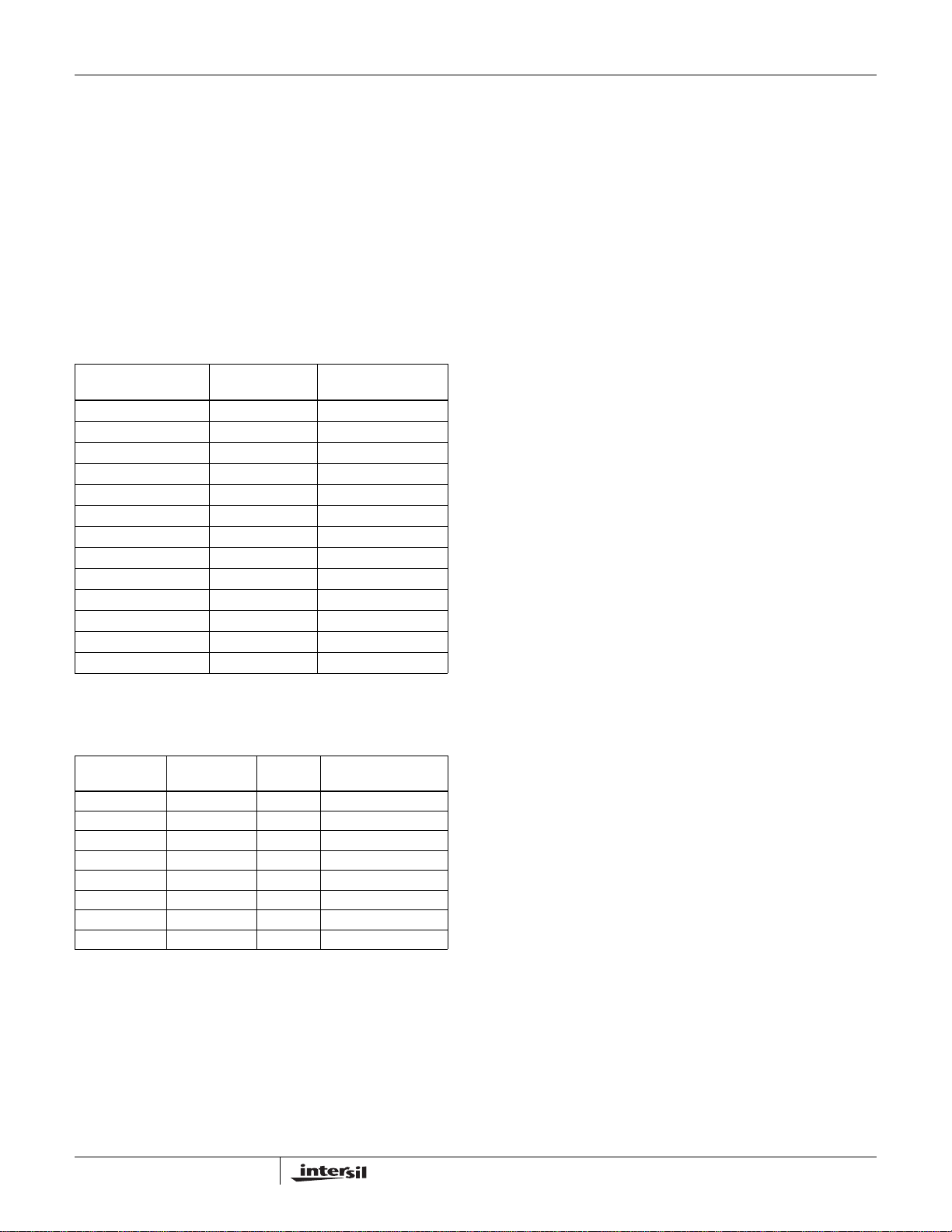
Cascade Input
When in the complex cascade mode the 4-channel summer
re 1 and im 1 are summed with the real and imaginary
cascade inputs. The cascade input allows for more than four
multi-channel transmissions by summing the complex
modulated signals from other device’s. A cascade chain of
four devices allows up to sixteen carriers. Figure 15
illustrates cascading multiple devices. Each device delays it’ s
4-channel summation to align with the cascade in from the
previous device. Device Control 0x78, bits 2:1 identifies the
position in the cascade chain. Device Control 0x78, bit 3
zeroes the cascade-in data when the port is not in use. The
output of the summation is saturated to prevent roll-over.
µP
µP
µP
µP
SCLKX
FSRX
SDX
SCLKX
FSRX
SDX
SCLKX
FSRX
SDX
SCLKX
FSRX
SDX
MASTER
ISL5217
QPUC
SLAVE
ISL5217
QPUC
SLAVE
ISL5217
QPUC
SLAVE
ISL5217
QPUC
I OUT <19:0>
Q OUT <19:0>
SYNCO
UPDX
Q IN <19:0>
I IN <19:0>
I OUT <19:0>
Q OUT <19:0>
UPDX
Q IN <19:0>
I IN <19:0>
I OUT <19:0>
Q OUT <19:0>
UPDX
Q IN <19:0>
I IN <19:0>
I OUT <19:0>
Q OUT <19:0>
ISL5217
<19:0>
I IN<19:0>
CASZ
MOD(20:0)
QIN
20
IOUT
<19:0>
R
22
E
G
>
21
R
E
G
>
∑
SATURATE
CIRCUITRY
QOUT
<19:0>
20
I OUT<19:0>
† ALL REGISTERS ARE CLOCKED AT CLK
FIGURE 16. CASCADE INPUT BLOCK DIAGRAM
Output Formatter
The output can be formatted in either twos complement or
offset binary. The OFFBIN pin is used to select the output
format. The output ranges from 0x8001 to 0x7FFF for two’s
complement and from 0x0001 - 0xFFFF for offset binary.
Microprocessor Interface
NOTE: See Appendix A, Errata Sheet
The microprocessor interface allows the QPUC to appear as
a memory mapped peripheral to the µP. Configuration data,
I/Q sample data and RAM data can be accessed through
this interface. The interface consists of a 16 bit bidirectional
data bus, P<15:0>, seven bit address bus, A<6:0>, a write
strobe (WR
Two µP interface modes are supported through the input pin
RDMODE
read and write strobe inputs. When high the device is
configured for a common Read/Write
This mode redefines RD
into Data Strobe.
), a read strobe (RD) and a chip enable (CE).
. When low the device is configured for separate
and data strobe inputs.
into Read/Write Strobe and WR
FIGURE 15. CASCADED QPUCs
The address space is partitioned into five directly accessible
regions, one for top control and one for each of the four
channels. The Device Control space allows for configuration
parameters that effect the entire device, cascade, output
modes, and routing. The channel space allows for
configuration parameters and sample data.
The master registers for the configuration data and I/Q
sample data are located in these areas. There is a master
16
FN6004.3
July 8, 2005
Page 17

ISL5217
www.BDTIC.com/Intersil
register and slave register pair for each configuration
parameter and I/Q sample. The slave register for the I/Q
samples is the first location of the FIFO. The master
registers are clocked by the µP write strobe, are writable and
cleared by a hard reset. The slave registers are clocked by
device clock, are readable and cleared by either a hard or
soft reset. The transfer of configuration data from the master
register to the slave register can occur synchronously after
an event or immediately after a four clock synchronization
period.
Indirect addressing is used to access the gain profile RAM,
the I coefficients RAM and the Q coefficients RAM. This type
of access relies on loading the RAM data into direct address
0x14 and the RAM address into direct address 0x15. After a
four clock synchronization period of the decoded address
0x15, the contents of the RAM data register is moved to the
address pointed to by the RAM address register. The µP can
perform back-to-back accesses to the RAM data register and
RAM address register, but must maintain four f
between accesses to the same address. This limits the
maximum µP access rate for the RAM to
104MHz/4 = 26MHz. The RAM address register defines a
16-bit address space that is partitioned into pages of 256
words by indirect address <9:8>. Indirect address<15>
determines the access type, 1 = read; 0 = write.
The address map and bit field details for the microprocessor
interface is shown in the Tables 10-47. The procedures for
reading and writing to this interface are provided below.
CLK
periods
Microprocessor Read/Write Procedure
The QPUC offers the microprocessor read/write access to all
of the configuration working registers, the gain profile RAM,
the I coefficients RAM and the Q coefficients RAM.
RDMODE determines the read/write mode for the
microprocessor interface as detailed in the pin description
table. The following e xamples hav e RDMODE set low, which
configures the interface for separate RD
and WR strobes.
Configuration Read/Write Procedure
Write Access to the Configuration Master
Registers
Perform a direct write to the configuration master registers
by setting up the address A<6:0>, data P<15:0>, and
generating WR
sequence is as shown. The order of writing to the de vice
should be maintained as:
strobe. The overal l con figur ation loa ding
5. Repeat steps 2-4 for all channels.
6. Write control word 0x0c to the final configuration values.
RDMODE
RD
WR
A<6:0> 0xc
P<15:0>
FIGURE 17. CONFIGURATION WRITE TRANSFER
0x78 0x2 0x3
9000
0x4 0x5
Read Access to the Configuration Slave Registers
1. Perform a direct read of a configuration register by
dropping the RD
selected by A<6:0> onto the data bus P<15:0>.
RDMODE
RD
WR
A<6:0>
P<15:0>
FIGURE 18. CONFIGURATION READ TRANSFER
line low to transfer data from the register
0XC 0X78 0X2 0X3 0X4 0X5
HI-Z
DATA VALID
I/Q Sample Read/Write Procedure
Write Access to the I/Q Sample Master Registers
2. Enable the parallel input format by clearing bit 15 of the
Serial control register, 0x11.
3. Perform a direct write to Control word 1 by setting up th e
address A<6:0>, data P<15:0>, and generating a rising
edge on WR.
4. Perform a direct write to Control word 0 by setting up th e
address A<6:0>, data P<15:0>, and generating a rising
edge on WR.
I/Q master registers to the first location of the FIFO.
5. Wait 4 clock cycles before performing the next write to the
Q data master register.
Read Access to the I/Q Sample Slave Registers
1. Perform a direct read of the I slave register by dropping
the RD
selected by A<6:0> onto the data bus P<15:0>.
A write strobe transfers the contents of the
line low to transfer data from the slave register
1. Write the Main Control register 0x0c. 0x9000 sets the
immediate update and microprocessor hold bits.
2. Write Device Control 0x78, bit 0 to set the broadcast bit if
writing to multiple channels. Set to 0 when writing to a
single channel.
3. Write all remaining registers sequentially .
4. Load all filter and gain coefficients.
17
FN6004.3
July 8, 2005
Page 18

ISL5217
www.BDTIC.com/Intersil
Gain Profile RAM Read/Write Procedure
Write Access to the Gain Profile RAM
1. Enable the gain profile hold mode by setting bit 14 of the
Main Control register 0x0c.
2. Load the RAM data to location 0x14.
3. Load the RAM write address to location 0x15. A write
strobe transfers the contents of the register at location
0x14 into the RAM location specified by the contents of
the register at location 0x15. (Indirect address[15] =0).
4. Wait 4 clock cycles bef ore performing the next write to the
RAM data register.
5. Repeat steps 2-4.
6. Return gain control back to the channel by disabling the
gain profile hold 0x0c, bit 14.
Read Access to the Gain Profile
1. Enable the gain profile hold mode by setting bit 14 of the
Main Control register 0x0c.
2. Load the RAM read address and 0x8000 to location 0x15.
A read strobe transfers the contents of the RAM location
specified by the contents of the register at location 0x15
onto the read bus. (Indirect address[15] =1, Indirect
address[9:8] =’00’).
3. Wait 4 clock cycles bef ore performing the next write to the
RAM address register.
4. Repeat steps 2-3.
5. Return gain control back to the channel by disabling the
gain profile hold 0x0c, bit 14.
Write Access to the Coefficient RAMs When I
Equal Q
1. Enable the µP hold mode by setting bit 12 of the Main
Control register 0x0c.
2. Load the RAM data to location 0x14 with the coefficient.
3. Load the RAM write address to location 0x15. A write
strobe transfers the contents of the register at location
0x14 into the RAM location specified by the contents of
the register at location 0x15. (Indirect address[15] =0,
Indirect address[9:8] =’11’).
4. Wait 4 clock cycles before performing the next write to the
RAM data register.
5. Repeat steps 2-4.
6. Return RAM control back to the channel by disabling the
µP hold mode.
Read Access to the I Coefficient RAM
1. Enable the µP hold mode by setting bit 12 of the Main
Control register 0x0c.
2. Load the RAM read address and 0x8100 to location 0x15.
A read strobe transfers the contents of the RAM location
specified by the contents of the register at location 0x15
onto the read bus. (Indirect address[15] =1, Indirect
address[9:8] =’01’).
3. Wait 4 clock cycles before performing the next write to the
Ram address register.
4. Repeat steps 2-3.
5. Return RAM control back to the channel by disabling the
µP hold mode.
Coefficients RAM Read/Write Procedure
(16-bit 2’s Complement Format)
The RAM address used for the I and Q coefficient RAM
depends on the filter. Indirect page 3 is used when the
coefficients are equal. When the coefficients are not equal
indirect page 1 is used.
Write Access to the Coefficient RAMs When I Not
Equal Q
1. Enable the µP hold mode by setting bit 12 of the Main
Control register 0x0c.
2. Load the RAM data to location 0x14 with the Q
coefficient.
3. Load the RAM data to location 0x14 with the I coefficient.
4. Load the RAM write address to location 0x15. A write
strobe transfers the contents of the register at location
0x14 into the RAM location specified by the contents of
the register at location 0x15. (Indirect address[15] =0,
Indirect address[9:8] =’01’).
5. Wait 4 clock cycles bef ore performing the next write to the
RAM data register.
6. Repeat steps 2-5.
7. Return RAM control back to the channel by disabling the
µP hold mode.
Read Access to the Q Coefficient RAM
1. Enable the µP hold mode by setting bit 12 of the Main
Control register 0x0c.
2. Load the RAM read address and 0x8200 to location 0x15.
A read strobe transfers the contents of the RAM location
specified by the contents of the register at location 0x15
onto the read bus. (Indirect address[15] =1, Indirect
address[9:8] =’10’).
3. Wait 4 clock cycles before performing the next write to the
RAM address register.
4. After all data has been loaded, return RAM control back
to the channel by disabling the µP hold mode.
Coefficients RAM Read/Write Procedure
(24-bit Floating Point Format)
The 24-bit floating point mode must be enabled by setting bit
12 of control word 0x17. The I and Q coefficients must be
loaded separately in this mode.
Write access to the Coefficient RAMs
1. Enable the µP hold mode by setting bit 12 of the Main
Control register 0x0c and bit 12 of the Test Control
register 0x17.
2. Load the RAM data to location 0x14 with the iCoef<3:0>,
iShift<3:0>, qCoef<3:0>, qShift<3:0>.
18
FN6004.3
July 8, 2005
Page 19

ISL5217
www.BDTIC.com/Intersil
3. Load the RAM data to location 0x14 with the
qCoef<19:4>.
4. Load the RAM data to location 0x14 with the
iCoef<19:4>.
5. Load the RAM write address to location 0x15. A write
strobe transfers the contents of the three previously
loaded registers at location 0x14 into the RAM location
specified by the contents of the register at location 0x15.
(Indirect address[15] =0, Indirect address[9:8] =’01’).
6. Wait 4 clock cycles bef ore performing the next write to the
RAM data register.
7. Repeat steps 2-6.
8. Return RAM control back to the channel by disabling the
µP hold mode.
Read Access to the Coefficient RAM
1. Enable the µP hold mode by setting bit 12 of the Main
Control register 0x0c and bit 12 of the Test Control
register 0x17.
2. Load the RAM read address and 0x8X00 to location 0x15.
Three read strobes are required to transfers the contents
of the RAM location specified by the contents of the
register at location 0x15 onto the read bus. Indirect
address[15] =1, Indirect address[9:8] =’01’, reads back the
iCoef value, Indirect address[15] =1, Indirect address[9:8]
=’10’, reads back the qCoef valu e, Indirect address[15] =1,
Indirect address[9:8] =’11’, reads back the iCoef<3:0>,
iShift<3:0>, qCoef<3:0>, qShift<3:0> value.
3. Wait 4 cloc k cyc les between all of the above writes before
performing the next write to the Ram address register.
4. Repeat steps 2-3.
5. Return RAM control back to the channel by disabling the
µP hold mode.
Channel Status
The present status of the channel is latched by the single
channel µP interface into the Status 0x16 register bits 11:0.
These bits represent the channel flushed, FIR and FIFO
overflow/underflow, FIFO read address, and FIFO almost and
empty flags. 0x16 bits 10:7 and bit 3 are or’ed and latched into
the Device Top Control 0x7e. The bits in 0x7e represent the
fault status of each channel and the saturation status of each
summer. The detection of a FIFO overflow puts the channel in
the off-line mode, unless disabled by assertion of 0x0c, bit 1.
The off-line function takes the channel off-line by forcing the
FIFO read address to ‘000’, which forces 0 data out of the FIFO.
The channel flushed status bit in control word 0x16, may be
monitored to find out when the zeroes have propagated through
the entire channel pipeline chain. The channel flushed status is
asserted 24 sample clocks after entering the off-line mode.
Once a channel fault is latched into the T op control 0x7e, 15:12
a write to this location is required to clear the faulted status.
Reset
There are two types of resets, a hard reset and a soft reset.
A hard reset can occur by asserting the input pin RESET
, or
by the µP issuing a reset command to the top control register
0x7F, bit 1. A hard reset affects the entire device, leaving the
QPUC in an idle state awaiting configuration. This type of
reset returns the master and slave registers to their default
values, clears the FIFO pointer, the NCO accumulators, the
RAM pointers, and zeroes the data RAM. The data RAM
locations are written with a zero value immediately after the
reset is deasserted.
A soft reset occurs by the µP issuing a reset command to the
channel’s immediate action control register 0xF, bit 1. A soft
reset is similar to the hard reset but does not clear the
master registers and its action is limited only to that channel.
A soft reset leaves the channel in an idle state, awaiting an
update to begin processing.
Update Control
There are several mechanisms for updating slave registers
from the master registers. If hardware UPDX
be used the following control bits should be programmed:
1. Main control register 0x0c bit 5 must be set to 1 to enable
hardware TXENX and UPDX.
2. Serial control register 0x11 bits 7:6 should be
programmed to configure which TXENX
respond to.
3. Serial control register 0x11 bits 5:4 should be
programmed to configure which UPDX a channel will
respond to.
4. Update Mask control register 0x0e bits 10:1 should be set
to configure which slave registers will be updated from
their corresponding master registers upon a nonimmediate channel update. Those registers with their
update mask bit set to 1 are enabled registers.
The 6 update mechanisms that are described below cause
the slave registers to be updated from the contents of the
corresponding master register.
1. Immediate Update - Set bit 15 of cword 0x0c to a 1 to
implement this mode. In immediate update mode, the
slave register is updated 4 CLKS after the master register
is written (update mask register is ignored).
2. Hardware Update - If the channel hardware update is
enabled, upon assertion of UPDX
registers are updated.
3. Software Update - Upon assertion of a channel software
update (bit 0 of control register 0x0f), the enabled slave
registers are updated.
4. External Hardware TXENX
hardware txEnable is enabled, upon assertion of TXENX
the enabled slave registers are updated.
5. Internal Hardware TXENX Assertion - If the internal
hardware txEnable function is enabled (bit 5 of cword
0x0c), upon assertion of the internal TXENX
by either type of dynamic channel update as described in
items 3 and 4 above), the enabled slave registers are
updated.
Assertion - If the channel
and TXENX will
a channel will
, the enabled slave
(kicked off
,
19
FN6004.3
July 8, 2005
Page 20

ISL5217
www.BDTIC.com/Intersil
6. Software TXENX Assertion - Upon assertion of a channel
software TXENX (bit 0 of cword 0x0c), the enabled sla v e
registers are updated.
Starting Sequence
Channel processing begins when the slave register of the
sample frequency and the interpolation phase are updated
with a non-zero value. The sample rate NCO provides the
timing strobes that drive the channel processing logic.
The starting sequence can be applied to one channel,
multiple channels, and multiple devices.
When starting multiple channels through a software update,
a broadcast write, to an immediate action register in the
channel address space asserts an update strobe.
When starting multiple QPUCs through a software update, a
write to the top control immediate action register, 0x78, bit 15
asserts the SYNCO pin. The first chip acts as a master and
is tied to an UPDX
A delayed starting sequence of a channel can be realized by
taking advantage of the On line mode defined in Main control
(0xc, bit 6). The On line mode allows µP access to the
RAM’s and allows the NCO’s to operate normally but inhibits
processing by forcing the FIFO data to zero.
pin of the remaining chips.
not at specified levels. During the power-up and power-do wn
operations, differences in the starting point and ramp rates of
the two supplies may cause current to flow in the isolation
structures which, when prolonged and excessive, can
reduce the usable life of the device. In general, the most
preferred case would be to power-up or down the core and
I/O structures simultaneously. However, it is also safe to
power-up the core prior to the I/O block if simultaneous
application of the supplies is not possible. In this case, the
I/O voltage should be applied within 10 ms to 100 ms
nominally to preserve component reliability. Bringing the
core and I/O supplies to their respective regulation levels in a
maximum time frame of a 100 ms, moderates the stresses
placed on both the power supply and the ISL5217. When
powering down, simultaneous removal is preferred, but It is
also safe to remove the I/O supply prior to the core supply. If
the core power is removed first, the I/O supply should also
be removed within 10-100mS.
JTAG and Built in Self Test
JTAG: The IEEE 1149.1 Joint Test Action Group boundary
scan standard operational codes shown in Table 9 are
supported. A separate application note is available with
implementation details and the BSDL file is available.
TABLE 9. JTAG OP CODES SUPPORTED
INSTRUCTION OP CODE
EXTEST 0000
IDCODE 0001
SAMPLE/PRELOAD 0010
INTEST 0011
BYPASS 1111
Self test is initiated by resetting the part and then loading a
given configuration register set, filter coefficient set, and gain
profile ramp. Control word 0x78, bit 14 should be set to 1 to
enter the self test mode. Upon assertion of a channel 0
update anded with updateMask bit 15, the device will begin
computing a signature which may then be read back from
control word 0x7d, bits <14:3>. Control word 0x7d, bit 15
reflects the validity (completion) of the test. This bit will be
cleared upon assertion of the 0x78, bit 14 test mode bit or
upon assertion of the channel 0 update and will be set to 1
upon completion of the test.
Po wer-up Sequencing
The ISL5217 core and I/O blocks are isolated by structures
which may become forward biased if the supply v oltages are
20
FN6004.3
July 8, 2005
Page 21

ISL5217
www.BDTIC.com/Intersil
Absolute Maximum Ratings Thermal Information
Supply Voltage. . . . . . . . . . . . . . . . . . . . . . . . . . . . . . . . . . . . . +3.8V
Input, Output or I/O Voltage. . . . . . . . . . . .GND -0.5V to V
ESD Classification . . . . . . . . . . . . . . . . . . . . . . . . . . . . . . . . . Class I
CC
+0.5V
Operating Conditions
Voltage Range Core, V
Voltage Range I/O, V
Temperature Range
Industrial. . . . . . . . . . . . . . . . . . . . . . . . . . . . . . . -40
Input Low Voltage . . . . . . . . . . . . . . . . . . . . . . . . . . . . . 0V to +0.8V
Input High Voltage . . . . . . . . . . . . . . . . . . . . . . . . . . . . . . .2V to V
CAUTION: Stresses above those listed in “Absolute Maximum Ratings” may cause permanent damage to the device. This is a stress only rating and operation of the
device at these or any other conditions above those indicated in the operational sections of this specification is not implied.
NOTES:
is measured in free air with the component mounted on a high effective thermal conductivity test board with “direct attach” features. S ee T ech
1. θ
JA
Brief TB379.
2. Single supply operation of both the core VCCC and I/O VCCIO at 2.5V is allowed. Degradation of the I/O timing should be expected.
3. Tie 196CABGA package rows F, G, H, and J pins 6-9 to heat sink or ground to ensure maximum device heat dissipation.
. . . . . . . . . . . . . . . . . . . .+2.4V to +2.6V
CCC
(Note 2). . . . . . . . . . . +3.15V to +3.45V
CCCIO
o
C to 85oC
CC
Thermal Resistance (Typical, Notes 1, 3) θ
JA
(oC/W)
196 Lead BGA Package. . . . . . . . . . . . . . . . . . . . . . 33
w/200 LFM Air Flow . . . . . . . . . . . . . . . . . . . . . . . . . 29
w/400 LFM Air Flow . . . . . . . . . . . . . . . . . . . . . . . . . 27
Maximum Package Power Dissipation at 85
196 Lead BGA Package. . . . . . . . . . . . . . . . . . . . . . . . . . . .1.97W
Maximum Storage Temperature Range. . . . . . . . . . -65
o
C
o
C to 150oC
Maximum Junction Temperature . . . . . . . . . . . . . . . . . . . . . . 150
Maximum Lead Temperature (Soldering 10s) . . . . . . . . . . . . 300
o
o
C
C
DC Electrical Specifications V
= 2.5 ± 5%, V
CCC
= 3.3 ±5%, TA = -40oC to 85oC
CCIO
PARAMETER SYMBOL TEST CONDITIONS MIN MAX UNITS
Logical One Input Voltage V
Logical Zero Input Voltage V
Clock Input High V
Clock Input Low V
Output High Voltage V
Output Low Voltage V
Input Leakage Current I
Output Leakage Current I
Input Pull-up Leakage Current Low I
Input Pull-up Leakage Current High I
Standby Power Supply Current I
Operating Power Supply Current I
CCOP
Input Capacitance C
IH
IL
IHC
IHL
OH
OL
L
H
SL
SH
CCSB
IN
= 2.6V, V
CCC
V
= 2.4V, V
CCC
V
= 2.6V, V
CCC
V
= 2.4V, V
CCC
IOH = -2mA, V
IOL = 2mA, V
VIN = V
CCIO
VIN = V
CCIO
VIN = V
CCIO
TMS, TRST
VIN = V
TMS, TRST
V
CCC
, TDI
CCIO
, TDI
= 2.6V, V
f = 80MHz, VIN = V
V
= 3.45V, V
CCIO
Freq = 1MHz, V
= 3.45V 2.0 - V
CCIO
= 3.15V - 0.8 V
CCIO
= 3.45V 2.0 - V
CCIO
= 3.15V - 0.8 V
CCIO
= 2.4V, V
CCC
= 2.4V, V
CCC
or GND, V
or GND, V
or GND, V
or GND, V
CCC
CCC
CCC
CCC
= 3.45V, Outputs Not Loaded - 5 mA
CCIO
or GND,
CCIO
= 2.6V
CCC
Open, All Measurements Are
CCIO
V
Referenced to Device Ground
Output Capacitance C
OUT
Freq = 1MHz, V
Referenced to Device Ground
Open, All Measurements are
CCIO
NOTES:
4. Power Supply current is proportional to operation frequency. Typical rating for I
5. Capacitance T
= 25oC, controlled via design or process parameters and not directly tested. Characterized upon initial design and at major
A
process or design changes.
= 3.15V 2.6 - V
CCIO
= 3.15V 0.4 V
CCIO
= 2.6V, V
= 2.6V, V
= 2.6V, V
= 2.6V, V
= 3.45V -10 10 µA
CCIO
= 3.45V -10 10 µA
CCIO
CCIO
CCIO
= 3.45V,
= 3.45V,
-500 - µA
-10 µA
- 540 mA (Note 4)
- 7 pF (Note 5)
- 7 pF (Note 5)
is 7mA/MHz.
CCOP
21
FN6004.3
July 8, 2005
Page 22

ISL5217
www.BDTIC.com/Intersil
AC Electrical Specifications V
= 2.5 ± 5%, V
CCC
= 3.3 ± 5%, TA = -40oC to 85oC (Note 6)
CCIO
PARAMETER SYMBOL MIN MAX UNITS
CLK Frequency f
CLK Clock Period t
CLK High t
CLK Low t
Setup Time IIN<19:0> or QIN<19:0> to CLK t
Hold Time IIN<19:0> or QIN<19:0> from CLK t
Setup Time TXENX
to CLK t
Hold Time TXENX from CLK t
Setup Time UPDX
Hold Time UPDX
to CLK t
from CLK t
Setup Time RESET High to CLK t
Hold RESET
RESET
High from CLK (Note 7) t
Low Pulse Width (Note 7) t
WR Pulse Width High t
Pulse Width Low t
WR
Pulse Width Low (RDMODE=1) t
WR
Setup Time A<6:0> to WR
Hold Time A<6:0> from WR t
Setup Time CS
Hold Time CS
to WR t
from WR t
Setup Time P<15:0> to WR t
Hold Time P<15:0> from WR
Enable P<15:0> from RD
(Note 5) t
Disable P<15:0> from RD (Note 5) t
Setup Time RD
Hold Time RD
Setup Time A<6:0> to WR
Hold Time A<6:0> from WR
Setup Time CS
Hold Time CS
Setup Time P<15:0> to WR
Hold Time P<15:0> from WR
Enable P<15:0> from WR
Disable P<15:0> from WR
Setup Time SDX
Hold Time SDX
to WR (RDMODE=1) (Note 7) t
from WR (RDMODE=1) (Note 7) t
(RDMODE=1) t
(RDMODE=1) t
to WR (RDMODE=1) t
from WR (RDMODE=1) t
(RDMODE=1) t
(RDMODE=1) t
or RD (RDMODE=1) (Note 7) t
or RD (RDMODE=1) (Note 7) t
to SCLKX t
from SCLKX t
PEWR1
PDWR1
CLK
CLK
CH
CL
IQISC
IQIHC
TSC
THC
USC
UHC
RSC
RHC
RPW
WPWH
WPWL
WPL1
t
ASW
AHW
CSW
CHW
PSW
t
PHW
PER
PDR
RSW1
RHW1
ASW1
AHW1
CSW1
CHW1
PSW1
PHW1
SSS
SHS
- 104 MHz
9.6 - ns
3- ns
3- ns
5- ns
0- ns
4- ns
0- ns
4- ns
0- ns
4- ns
1- ns
10 - CLK Cycles
5- ns
5- ns
6- ns
10 - ns
0- ns
4- ns
0- ns
8- ns
0- ns
-6 ns
-6 ns
0- ns
0- ns
10 - ns
0- ns
4- ns
0- ns
8- ns
0- ns
-6 ns
-6 ns
8- ns
0- ns
IOUT<19:0> or QOUT<19:0> Enable Time from OUTEN<1:0> (Note 7) tIQOE - 7 ns
IIN<19:0> or QIN<19:0> Enable Time from CLK (Note 7) t
IQIE
-8 ns
IOUT<19:0> or QOUT<19:0> Disable Time from OUTEN<1:0> (Note 7) tIQOD - 6 ns
IIN<19:0> or QIN<19:0> Disable Time from CLK (Note 7) t
IQID
-7 ns
22
FN6004.3
July 8, 2005
Page 23

ISL5217
www.BDTIC.com/Intersil
AC Electrical Specifications V
= 2.5 ± 5%, V
CCC
= 3.3 ± 5%, TA = -40oC to 85oC (Note 6) (Continued)
CCIO
PARAMETER SYMBOL MIN MAX UNITS
IIN<19:0> or QIN<19:0> Delay Time from CLK t
IOUT<19:0> or QOUT<19:0> Delay Time from CLK t
IIN<19:0> or QIN<19:0> Valid Time from CLK, 2X Rate t
IOUT<19:0> or QOUT<19:0> Valid Time from CLK, 2X Rate t
Valid Time from CLK, SCLX = CLK t
SCLKX
Valid Time from CLK, SCLX = Divided CLK tSVC 2 7 ns
SCLKX
ISTRB Delay Time from CLK t
Delay Time from CLK t
FSRX
SYNCO Delay Time from CLK t
P<15:0> Delay Time from CLK t
P<15:0> Delay Time from A<6:0> or CS
P<15:0> Delay Time from A<6:0> or CS
(RDMODE=1) t
Output Rise/Fall Time (Note 7) t
IQIDC
IQODC
IQVC2X
IQVC2X
SVC1X
IDC
FDC
SDC
PDC
t
PDAC
PDAC1
RF
27 ns
27 ns
28 ns
28 ns
27 ns
26 ns
-7 ns
-9 ns
-16 ns
-20 ns
-20 ns
-3 ns
NOTES:
6. AC tests performed with C
Test V
= 3.0V, V
IH
IHC
= 70pF. Input reference level for CLK is 1.5V, all other inputs 1.5V.
L
= 3.0V, VIL = 0V, VOL = 1.5V, VOH = 1.5V.
7. Controlled via design or process parameters and not directly tested. Characterized upon initial design and at major process or design changes.
AC Test Load Circuit
Waveforms
t
CLK
tCHt
CL
CLK
t
RHC
DUT
SWITCH S1 OPEN FOR I
† TEST HEAD CAPACIT ANCE
t
= 1 / F
CLK
t
CLK
RPW
CCSB
t
RSC
C
L
AND I
S
1
†
±
1.5V I
t
SSS
OL
t
SVC
t
FDC
t
SHS
CCOP
I
OH
EQUIVALENT CIRCUIT
CLK
SCLKX
FSRX
RESET
SDX
FIGURE 19. CLOCK AND RESET TIMING FIGURE 20. SERIAL INTERFACE RELATIVE TIMING
23
FN6004.3
July 8, 2005
Page 24

Waveforms (Continued)
www.BDTIC.com/Intersil
ISL5217
CLK
IN<19:0>,
QIN<19:0>
SYNCO
ISTRB
P<15:0>
UPDX,
TXENX
CLK
IIN<19:0>,
QIN<19:0>,
IOUT<19:0>,
QOUT<19:0>
t
IQISC
t
SDC
t
PDC
VALID
VALID
t
IDC
t
IQIHC
VALID
t
USC, tTSC
t
UHC, tTHC
CLK
t
IQIE
IIN<19:0>,
QIN<19:0>
OUTEN<1:0>
t
IQOD
IOUT<19:0>,
QOUT<19:0>
t
IQOE
t
IQID
FIGURE 21. INPUT/OUTPUT TIMING FIGURE 22. ENABLE/DISABLE TIMING
CLK
t
IQVC2X
SCLKX
t
SVC1X
t
IQIDC
t
IQODC
FIGURE 23. MUXED IQ AT 2X OUTPUT TIMING FIGURE 24. SCLKX
RD (RD/WR)
RD
WR
CS
A<6:0>
P<15:0>
t
WPWL
VALID
VALID
t
WPWH
t
CSW
t
t
ASW
t
t
PSW
t
WR (DS)
CHW
CS
AHW
A<6:0>
PHW
P<15:0>
OUTPUT TIMING IN 1X MODE
t
RSW1
t
WPWL1
t
CSW1
t
ASW1
VALID
t
PSW1
VALID
t
RHW1
t
t
AHW1
t
CHW1
PHW1
FIGURE 25. MICROPROCESSOR WRITE TIMING (RDMODE = 0) FIGURE 26. MICROPROCESSOR WRITE TIMING (RDMODE= 1)
24
FN6004.3
July 8, 2005
Page 25

Waveforms (Continued)
www.BDTIC.com/Intersil
ISL5217
RD
WR
CS
A<6:0>
P<15:0>
FIGURE 27. MICROPROCESSOR READ TIMING (RDMODE = 0) FIGURE 28. MICROPROCESSOR READ TIMING (RDMODE = 1)
VALID
t
PDAC
t
PER
VALID
t
PDR
RD (RD/WR)
WR (DS)
CS
A<6:0>
P<15:0>
t
PEWR1
t
PDAC1
VALID
VALID
t
PDWR1
Programming Information
TABLE 10. ISL5217 MEMORY MAP
ADDRESS(6:0) DEVICE MEMORY MAP
(000 0000) - (001 0111)
0x00 - 0x17
(001 1000) - (001 1111)
0x18 - 0x1f
(010 0000) - (011 0111)
0x20-0x37
(011 1000) - (011 1111)
0x38 - 0x3f
(100 0000) - (101 0111)
0x40-0x57
(101 1000) - (101 1111)
0x58 - 0x5f
(110 0000) - (111 0111)
0x60-0x77
(111 1000) - (111 1111)
0x78-0x7f
NOTES:
8. Consecutive accesses to the same address require a 4 clock synchronized update to occur before beginning the next accesses.
9. Different direct address locations can be accessed without having to wait for a 4 clock synchronized update to occur.
10. All configuration registers have a master/slave architecture. The master registers are clocked by WR
11. The master registers are writable and cleared by a hard reset. All master registers are located in the SC µP block.
12. The slave registers are readable and cleared by either a hard or soft reset. Refer to the table to determine location of slave registers.
13. Partition indirect address space into pages of 256 words.
14. Decode indirect address <9:8> to determine page, (3 used).
15. Indirect address<14:10> are not used.
16. Indirect address<15> determines access type. 1=read; 0=write.
Channel 0
Undefined
Channel 1
Undefined
Channel 2
Undefined
Channel 3
Device control
. The slave registers are clocked by CLK.
25
FN6004.3
July 8, 2005
Page 26

ISL5217
www.BDTIC.com/Intersil
Device Control Registers
TABLE 11. DEVICE CONTROL REGISTER MAP
UPDATE
ADDRESS (6:0) TYPE
11 1 1000 (0x78) R/W QC µP Intf Device Control <15:0>. 0x0000
11 1 1001 (0x79) R/W X QC µP Intf Device Output Routing Control <15:0>. 0x0000
11 1 1010 (0x7a) Not Used. 11 1 1011 (0x7b) Not Used. 11 1 1100 (0x7c) Not Used. 11 1 1101 (0x7d) R QC µP Intf Bist And Device Revision Code <15:0>. 0x0001
11 1 1110 (0x7e) R/W QC µP Intf Device Status <15:0>. 0x0000
11 1 1111 (0x7f) W N/A Device Immediate Action <15:0>. 0x0000
BIT FUNCTION DESCRIPTION
15 BIST Valid Reflects the validity of the Built In Self Test (BIST) signature. The bit is cleared upon assertion or de-
14:3 BIST Signature Built in self test resultant signature.
2:0 Revision Status Revision status currently 001.
NOTE: Bits listed as reserved should be set to 0 for backwards compatibility.
STROBE
assertion of the test mode bit in 0x78, bit 14, and set to one upon completion of the BIST. BIST signature
is valid when the bit is one.
SLAVE
LOCATION FUNCTION
TABLE 12. BIST and DEVICE REVISION
TYPE: DEVICE CONTROL DIRECT, ADDRESS: 0x7d
RESET
DEFAULT
TABLE 13. DEVICE STATUS
TYPE: DEVICE CONTROL DIRECT, ADDRESS: 0x7e
BIT FUNCTION DESCRIPTION
15 CH3 Summary Fault FIFO overflow or saturation detected.
14 CH2 Summary Fault FIFO overflow or saturation detected.
13 CH1 Summary Fault FIFO overflow or saturation detected.
12 CH0 Summary Fault FIFO overflow or saturation detected.
11 Output Summary Fault Saturation detected.
10 Reserved Not used.
9 Cascade I Sat Saturation detected, data saturates to most positive value or most negative value + 1.
8 Cascade Q Sat Saturation detected, data saturates to most positive value or most negative value + 1.
7 Output Summer 4, I Sat Saturation detected, data saturates to most positive value or most negative value + 1.
6 Output Summer 4, Q Sat Saturation detected, data saturates to most positive value or most negative value + 1.
5 Output Summer 3, I Sat Saturation detected, data saturates to most positive value or most negative value + 1.
4 Output Summer 3, Q Sat Saturation detected, data saturates to most positive value or most negative value + 1.
3 Output Summer 2, I Sat Saturation detected, data saturates to most positive value or most negative value + 1.
2 Output Summer 2, Q Sat Saturation detected, data saturates to most positive value or most negative value + 1.
1 Output Summer 1, I Sat Saturation detected, data saturates to most positive value or most negative value + 1.
0 Output Summer 1, Q Sat Saturation detected, data saturates to most positive value or most negative value + 1.
NOTES:
17. Channel summary fault is the logical or’ing of channel status <10:7,3>.
18. Clear fault by writing “1” to each summary fault bit (15:11).
19. Channel summary status is cleared as well as the Channel status word.
20. Output summary fault clears top status bits <9:0>.
26
FN6004.3
July 8, 2005
Page 27

ISL5217
www.BDTIC.com/Intersil
TABLE 14. DEVICE IMMEDIATE ACTION
TYPE: DEVICE CONTROL DIRECT, ADDRESS: 0x7f
BIT FUNCTION DESCRIPTION
15:2 Reserved Not Used.
1 Reset Hard Reset. Self clearing pulse zeroes data RAMs, returns master and slave configuration registers to
0 Sync Out Software Sync Out. Self clearing pulse used to synchronize multiple devices. See Figure 3.
their default values, etc. The device is in an idle state after reset.
Single Channel Direct Control Registers
TABLE 15. SINGLE CHANNEL DIRECT REGISTER MAP
DIRECT
ADDRESS
(4:0) TYPE
00 R/W X X FIFO I Channel Input or FM <15:0>. 01 R/W X FIFO Q Channel input <15:0>. 02 R/W Sample NCO Fixed Integer divider <31:16> MSW. 0x0000
03 R/W X Sample NCO Fixed Integer divider <15:0> LSW. 0x0000
04 R/W Sample NCO Sample Freq <47:32>, MSW. 0x0000
05 R/W Sample NCO Sample Freq <31:16>. 0x0000
06 R/W X Sample NCO Sample Freq <15:0>, LSW. 0x0000
07 R/W X Carrier NCO Carrier Freq static phase offset <15:0>. 0x0000
08 R/W Carrier NCO Carrier Freq MSW <15:0>. 0x0000
09 R/W X Carrier NCO Carrier Freq LSW <15:0>. 0x0000
0a R/W X Final Gain Gain <15:0>. 0x0000
0b R/W X µP Interface Gain Profile length <8:0>. 0x0000
0c R/W X µP Interface Main Control <15:0>. 0x0000
0d R/W X Timing and Cntrl,
0e R/W X µP Interface Update Mask <15:0>. 0x0000
0f W µP Interface Immediate Action<15:0>. 0x0000
10 R/W X µP Interface Polarity Control<15:0>. 0x0000
11 R/W X Timing and Cntrl,
12 R/W X Serial Interface I Serial Time slot<15:0>. 0x0000
13 R/W X Serial Interface Q Serial Time slot<15:0>. 0x0000
14 W µP Interface RAM Data <15:0>. 0x0000
15 W X µP Interface RAM Address <15:0>. 16 R µP Interface Status <15:0>. 0x0000
17 R/W X µP Interface Test Control<15:0>. 0x0000
18:1F Not Used. 0x0000
UPDATE
STROBE
ALWAYS
UPDATE
IMMEDIATE
SLAVE
LOCATION FUNCTION RESET DEFAULT
FIR Control <15:0>. 0x0000
Sample NCO,
IQ FIFO, FIR and
Gain
Serial Control <15:0>. 0x0000
Serial Interface
27
FN6004.3
July 8, 2005
Page 28

ISL5217
www.BDTIC.com/Intersil
TABLE 16. I CHANNEL INPUT OR FM (15:0)
TYPE: SINGLE CHANNEL DIRECT, ADDRESS: 0x00
BIT FUNCTION DESCRIPTION
15:0 I Channel QASK Input or
FM Input
BIT FUNCTION DESCRIPTION
15:0 Q Channel Input Q(15:0). In QASK mode, this is the Q input vector. See address 0 above. In FM mode, this input is not
NOTE: Writing to the I channel input generates the update strobe to move the data into the IQ FIFO. Normal write order is Q then I.
BIT FUNCTION DESCRIPTION
15:0 Fixed Integer Divider FID(31:16) is loaded in this address. See Address 3.
I(15:0). In QASK mode, this is the I input vector. The format is 2’s complement. The MSB is bit 15. The
mixer operation is:
OUT = (I*COS) - (Q*SIN).
In FM mode, this is interpreted as an offset frequency to the center frequency. The modulation index
depends on the mode and the filter coefficients. In FM with post filter mode, the phase change per input
sample can range from -180 to 180 degrees, so the deviation is limited to ±(input sample rate)/2.
TABLE 17. Q CHANNEL INPUT (15:0)
TYPE: SINGLE CHANNEL DIRECT, ADDRESS: 0x01
used.
TABLE 18. FIXED INTEGER DIVIDER, MSW
TYPE: SINGLE CHANNEL DIRECT, ADDRESS: 0x02
TABLE 19. FIXED INTEGER DIVIDER, LSW
TYPE: SINGLE CHANNEL DIRECT, ADDRESS: 0x03
BIT FUNCTION DESCRIPTION
15:0 Fixed Integer Divider FID(15:0) is loaded in this address. The fixed integer divider is a 32 bit counter clocked at the output clock
rate. The carryout is used to clear the fine and /or coarse phase of the sample rate NCO. Allows fixed
integer sample rates. The fixed integer divider is computed by the formula:
FID (31:0) = INT [fCLK/ fCO]
NOTE: Writing to the LSW generates the update strobe to load the slave configuration reg when in the immediate mode
TABLE 20. SAMPLE FREQUENCY (47:32) MSW
TYPE: SINGLE CHANNEL DIRECT, ADDRESS: 0x04
BIT FUNCTION DESCRIPTION
15:0 Sample Rate NCO SF(47:32) is loaded in this address. See Address 6.
TABLE 21. SAMPLE FREQUENCY (31:16)
TYPE: SINGLE CHANNEL DIRECT, ADDRESS: 0x05
BIT FUNCTION DESCRIPTION
15:0 Sample Rate NCO SF(31:16) is loaded in this address. See Address 6.
TABLE 22. SAMPLE FREQUENCY (15:0) LSW
TYPE: SINGLE CHANNEL DIRECT, ADDRESS: 0x06
BIT FUNCTION DESCRIPTION
15:0 Sample Rate NCO SF(15:0) is loaded in this address. The sample rate is controlled by a 48-bit NCO clocked at the output
NOTE: Writing to the LSW generates the update strobe to load the slave configuration reg when in the immediate mode.
clock rate. The sample rate is computed by the formula:
SF (47:0) = INT [(f
/ f
s
CLK
) * 2
48
]
28
FN6004.3
July 8, 2005
Page 29

ISL5217
www.BDTIC.com/Intersil
TABLE 23. CARRIER PHASE OFFSET (15:0)
TYPE: SINGLE CHANNEL DIRECT, ADDRESS: 0x07
BIT FUNCTION DESCRIPTION
15:0 Carrier Phase Offset Initializes the most-significant 16-bits of the phase accumulator. The carrier phase offset is computed by
the formula:
Carrier Phase Offset (15:0) = INT [(Phase Offset 0 / 3600 * 2
TABLE 24. CARRIER FREQUENCY (31:16) MSW
TYPE: SINGLE CHANNEL DIRECT, ADDRESS: 0x08
BIT FUNCTION DESCRIPTION
15:0 Carrier NCO CF(31:16) is loaded in this address.
TABLE 25. CARRIER FREQUENCY (15:0) LSW
TYPE: SINGLE CHANNEL DIRECT, ADDRESS: 0x09
BIT FUNCTION DESCRIPTION
15:0 Carrier NCO CF(15:0) is loaded in this address. The SIN/COS generator is controlled by a 32-bit NCO clocked at the
output clock rate. The center frequency is computed by the formula:
f
C = CF(31:0) x fCLK x 2
NOTE: Writing to the LSW generates the update strobe to load the slave configuration reg when in the immediate mode
-32
; CF(31:0) = INT(fC/fCLK X 232).
32
)) /216]
TABLE 26. GAIN
TYPE: SINGLE CHANNEL DIRECT, ADDRESS: 0x0a
BIT FUNCTION DESCRIPTION
15 Reserved Not Used.
14:12 Step Atten (2:0) Select 1 of 8 fixed attenuations
000 - scale by 4096
001 - scale by 256
010 - scale by 32
011 - scale by 16
100 - scale by 8
101 - scale by 4
110 - scale by 2
111 - scale by 1
11:0 Unsigned Gain Multiplier The gain multiplier is computed by the formula:
Gain(11:0) =[10
Bit weight. 2
Maximum 0xFFF = 1.0 - 2-12
0x800 = 0.5
0x001 = 2
Minimum 0x000 = 0.0
TYPE: SINGLE CHANNEL DIRECT, ADDRESS: 0x0b
BIT FUNCTION DESCRIPTION
8:7 Gain Profile Latency Set bit 7 high to remove two edge latencies from the delay path. This should be combined DS=3, IP=4
settings to provide perfect symmetry through the gain block. Set bit 8 high to bypass all latency alignment
circuitry and to use TXENX
6:0 Gain Profile Length Set to the upper address used for the gain profile RAM.
|(Gain(db)| / 20 )212
-1 2-2
-12
... 2
=0.9998
-12
TABLE 27. GAIN PROFILE
as input to the channel.
]Hex
29
FN6004.3
July 8, 2005
Page 30

ISL5217
www.BDTIC.com/Intersil
TABLE 28. MAIN CONTROL
TYPE: SINGLE CHANNEL DIRECT, ADDRESS: 0x0c
BIT FUNCTION DESCRIPTION
15 Immediate Update
(sc conf reg update)
14 Gain Profile Hold Allows µP access to the gain profile RAM. Upon assertion the device will hold the last address and gain
13 Delay Select 0 = no delay.
12 µP Hold Allows µP access to the I and Q coefficient RAMs.
11 TXENX
10:8 Almost Empty Threshold
7 Complex Output Mode Allows complex data out at the full rate when in 4-ch re output mode. The effect of this setting depends
Control Set to one to enable the internal generation and control of TXENX based on the programmed values of
(2:0)
0 = Allows the configuration slave registers to be synchronously updated based the update mask.
1 = Allows µP writes to bypass the update mask and load the selected configuration slave register
immediately from the master, (requires 4 clk synchronization).
value from the ramp. When deasserted, the gain profile RAM output returns to the ramp address and
value currently loaded. Normal access would be to re-load the coefficients with the gain profile RAM
ramping function having completed (either up or down).
0 = normal access by the hardware.
1 = µP access for loading the gain profile coefficients.
1 = 1/2 coarse sample delay inserted in the I/Q path after the FIR.
0 = normal access by the hardware.
1 = µP access for loading filter coefficients.
indirect registers 0x400-0x404 and 0x407. Set to zero (default) to input TXENX
Almost Empty Threshold (2:0). FIFO depth threshold (number of data samples in the FIFO - 1) at which
the Almost Empty flag will be asserted, alerting the data source that more input data is required in the
FIFO. The FIFO threshold sets both the I and Q FIFO thresholds. (2) is the MSB.
on the channel.
CH 0 = Over-rides selection of re sum2 and selects im sum1 for output.
CH 1 = n/a.
CH 2 = Over-rides selection of re sum4 and selects im sum3 for output.
CH 3 = n/a.
externally.
6 On-Line Mode 0 = Off line - zeroes data from FIFO - (reset FIFO cntrl forces rd_addr to 0 which selects zero value data
5 Input En Enables input of selected hw TX_enable and hw Update.
4 Channel Output En 0 = Disables output of channel, clears data to zero.
3 TXENX
2 TXENX
1 FIFO Overflow Reset Disables the FIFO overflow channel reset function. This is only applicable in the parallel input mode.
0 Sw TX Enable Rising edge flushes data RAM, (16 clks) and updates configuration slave registers as determined by the
SIB Control Disables TXENX control of the Serial Interface Block (SIB) and allows it to continue running independent
Channel Flush Disables TXENX control of the channel flushing. Setting this bit will stop the device from flushing the
for I and Q) This takes 24 sample-clocks to flush the channel. The status bit CH FLUSHED will be
asserted when complete.
1 = On line - allows normal operation of the IQ FIFO’s.
1 = Enables output of channel. Passes data.
of the TXENX
processed by the SIB.
0 = normal TXENX
1 = TXENX
channel and FIR data RAM with zeroes upon the rising edge of TXENX
0 = normal TXENX
1 = TXENX
0 = normal FIFO overflow channel reset.
1 = FIFO overflow channel reset disabled.
update mask. High level allows serial requests to occur. Low level inhibits additional serial data requests,
(assertion TX frame strobe).
signal. Data input should be zeroed during TXENX low time, as the data will continue to be
control of SIB.
SIB control disabled.
.
channel flushing.
will not flush the channel.
30
FN6004.3
July 8, 2005
Page 31

ISL5217
www.BDTIC.com/Intersil
TABLE 29. FIR CONTROL
TYPE: SINGLE CHANNEL DIRECT, ADDRESS: 0x0d
BIT FUNCTION DESCRIPTION
15 Gain Profile Mode Enables gain profile to slew gain value during transitions of TX enable
14 Clear Sample Phase When enabled will clear sample phase on immediate update of sample frequency
13 FM_Mode Disable Set to 1 to disable the internal FM_Mode signal to the serial interface block. This keeps the I/Q input
12 Fixed Integer Mode Enables the fixed integer divider in the sample rate NCO
11:10 Phase Offset (1:0) The phase accumulator of the sample rate NCO can be offset by increments of 90 degrees.
9 Half Band Filter Enable 0=Half Band filter bypassed (default).
8 Coefficient Switch Selects second filter coefficients in coefficient RAM.
7:4 Data Span (3:0) Data Span(3:0). Number of data samples in shaping filter, 4-16. Load with number of data samples minus
3:2 Modulation Type (1:0) Modulation type(1:0)
1:0 Interpolation Phases
(1:0)
NOTES:
21. QASK mode data flow - FIFO -> shaping filter -> interpolating filter
22. FM post mode data flow - FIFO -> FM modulator -> shaping filter -> interpolating filter
23. FM pre mode data flow - FIFO -> shaping filter -> FM modulator -> interpolating filter
24. The Q FIFO is not used when in the FM mode.
0 = maintain sample phase
1 = clear sample phase.
sample alignment such that the serial interface block expects both the I and Q time slot counters to count
down to 0 prior to transferring the I/Q samples to the FIFO. Loss of synchronization of the I/Q samples
can occur when switching FM modes without this bit set.
0
00 = 0
0
01 = 90
10 = 180
11 = 270
1=Half Band filter enabled.
1.
00 = QASK - PSK or QAM modulation.
01 = FM post-filtering - Analog FM modulation. Filtering after FM modulation (baseband filtering provided
before ISL5217). In this mode both I and Q filters are used.
10 = FM pre-filtering - FSK, GMSK modulation. Filtering before FM modulation. In this mode, only the I
filter is used.
11 = Invalid state.
Interpolation Phases(1:0) Number of coarse interpolation phases:
00 = forces coarse and fine phase to zero.
01 = 4.
10 = 8.
11 = 16.
0
0
TABLE 30. UPDATE MASK
TYPE: SINGLE CHANNEL DIRECT, ADDRESS: 0x0e
BIT FUNCTION DESCRIPTION
15 PN-Generator 1 = update, 0 = no update. PN-Generator is synchronously reset via the channel 0 UPDX
with this mask bit.
14:11 Reserved Not Used.
10 Serial Control,
I and Q Time Slot
9 FIR control
8Gain
7 Carrier Phase
6 Carrier Freq
1 = Update, 0 = No Update.
31
signal anded
FN6004.3
July 8, 2005
Page 32

ISL5217
www.BDTIC.com/Intersil
TABLE 30. UPDATE MASK (Continued)
TYPE: SINGLE CHANNEL DIRECT, ADDRESS: 0x0e
BIT FUNCTION DESCRIPTION
5 Sample Rate Divider
4 Sample Rate Freq
3 Sample Fine Phase
2 Sample Coarse Phase
1 Routing Control
0 I Strobe 1 = Update, 0 = No Update.
NOTES:
25. The mask register enables the slave registers to be updated from a hardware or software strobe.
26. The mask register is not used when µP is updating a configuration slave register immediately.
27. There is no immediate update on the I strobe.
28. Update mask <1> only affects the top routing control nibble for this channel.
TABLE 31. IMMEDIATE ACTION
TYPE: SINGLE CHANNEL DIRECT, ADDRESS: 0x0f
BIT FUNCTION DESCRIPTION
15:2 Reserved Not used
1 Soft Reset
(Channel Reset)
0 Software Update
(General Update)
Soft reset. Self clearing pulse zeroes FIFO’s, zeroes data RAMs, and clears all but the master registers.
The device will reload the slave configuration registers on the next TX enable or update strobe
Software update Self clearing pulse allows µP write to load all configuration slave registers synchronously
as determined by the update mask. The software equivalent of the hardware Update strobe
TABLE 32. POLARITY CONTROL
TYPE: SINGLE CHANNEL DIRECT, ADDRESS: 0x10
BIT FUNCTION DESCRIPTION
15:4 Reserved N/A
3 Tx Enable Polarity TX enable polarity
0 = defines an assertion as a transition from a logic low to a logic high
1 = defines an assertion as a transition from a logic high to a logic low
0 = 1 =
2 Update Polarity Update polarity.
1 FSR Polarity Frame strobe polarity.
0 Serial CLK Polarity Serial clk polarity.
0 = defines an assertion as a transition from a logic low to a logic high
1 = defines an assertion as a transition from a logic high to a logic low
0 = 1 =
0 = defines an assertion as a transition from a logic low to a logic high
1 = defines an assertion as a transition from a logic high to a logic low
0 = 1 =
0 = defines an assertion as a transition from a logic low to a logic high
1 = defines an assertion as a transition from a logic high to a logic low
0 = 1 =
32
FN6004.3
July 8, 2005
Page 33

ISL5217
www.BDTIC.com/Intersil
TABLE 33. SERIAL CONTROL (13:0)
TYPE: SINGLE CHANNEL DIRECT, ADDRESS: 0x11
BIT FUNCTION DESCRIPTION
15 Serial/parallel Data
Select
14 Epoch Frame Strobe
Enable
13:10 Serial Clock Rate (3:0) Clock divider to generate 1 of 16 serial clock rates
9:8 Serial Clock Mode (1:0) Selects the source for serial TX clock output.
7:6 Select TX Enable (1:0) Selects the TX enable port. The rising edge flushes data, (16 clks) and updates configuration slave
5:4 Select Update(1:0) Selects the Update port. The Update strobe is used to update all slave configuration registers as
3:2 Serial Word Length (1:0) Selects the word length of the incoming serial data The value is for one data word and is the same for
1:0 Select Serial Data in (1:0) Selects the serial data in port.
Selects the source of the symbol data for input.
0 = µP port, (parallel interface)
1 = serial port, (one of four serial ports)
Selects a pre-carry out of the fixed integer divider instead of the serial frame strobe. The pre-carry out is
six clocks ahead of the true carry out. This strobe is used to synchronize fixed integer dividers on other
devices.
0 = serial frame strobe.
1 = epoch frame strobe.
0000 = clk/2 1101 = clk/28
0001 = clk/4 1110 = clk/30
0010 = clk/6 1111 = clk/32
00 = Disables serial clock divider and serial clock out.
01 = Select 1x clock rate.
10 = Select divided clock rate.
11 = Select 32x sample clock rate.
registers as determined by the update mask. High level allows serial requests to occur. Low level inhibits
additional serial data requests, (assertion of TX frame strobe).
00 = TX enable A.
01 = TX enable B.
10 = TX enable C.
11 = TX enable D.
determined by the update mask.
00 = Update A.
01 = Update B.
10 = Update C.
11 = Update D.
both I and Q data.
00 = 16 bits.
01 = 12 bits.
10 = 8 bits.
11 = 4 bits.
00 = Serial data A.
01 = Serial data B.
10 = Serial data C.
11 = Serial data D.
TABLE 34. I - SERIAL TIME SLOT
TYPE: SINGLE CHANNEL DIRECT, ADDRESS: 0x12
BIT FUNCTION DESCRIPTION
15:10 Reserved Not Used.
9:0 I Time Slot(9:0) The
BIT FUNCTION DESCRIPTION
15:10 Reserved Not Used.
9:0 Q Time Slot (9:0) The
I - SERIAL TIME SLOT is a 10 bit counter clocked at the serial clock rate. The counter begins on
assertion of the Frame strobe. The carryout determines when a valid I symbol has been shifted in.
TABLE 35. Q - SERIAL TIME SLOT
TYPE: SINGLE CHANNEL DIRECT, ADDRESS: 0x13
Q - SERIAL TIME SLOT is a 10 bit counter clocked at the serial clock rate. The counter begins on
assertion of the Frame strobe. The carryout determines when a valid Q symbol has been shifted in.
33
FN6004.3
July 8, 2005
Page 34

ISL5217
www.BDTIC.com/Intersil
TABLE 35. Q - SERIAL TIME SLOT (Continued)
TYPE: SINGLE CHANNEL DIRECT, ADDRESS: 0x13
BIT FUNCTION DESCRIPTION
NOTES:
29. When in the QASK mode, the I and Q symbols will not be moved into the FIFO until both have been received.
30. When in the FM mode, the I symbol is moved to the FIFO after it has been shifted in.
31. The order of the I and Q symbols is based on the I and Q time slot values.
TABLE 36. RAM DATA (15:0)
TYPE: SINGLE CHANNEL DIRECT, ADDRESS: 0x14
BIT FUNCTION DESCRIPTION
15:0 RAM Data Indirect data port for the Gain profile, I and Q coefficients RAMs.
TABLE 37. RAM ADDRESS (15:0)
TYPE: SINGLE CHANNEL DIRECT, ADDRESS: 0x15
BIT FUNCTION DESCRIPTION
15:0 RAM Address Indirect address port for the Gain profile, I and Q coefficients RAMs. The MSB determines the type of
BIT FUNCTION DESCRIPTION
15:12 Reserved Not Used.
11 Channel Flushed Indicates zero valued data has propagated through the channel after entering the off-line mode. Counts
10 I FIR Overflow I FIR accumulator output saturates to most positive value.
9 I FIR Underflow I FIR accumulator output saturates to most negative value + 1.
8 Q FIR Overflow Q FIR accumulator output saturates to most positive value.
7 Q FIR Underflow Q FIR accumulator output saturates to most negative value + 1.
6:4 FIFO Read Address
<2:0>
3 FIFO Underflow FIFO read address = 0, FIFO write =0, FIFO read =1.
2 FIFO Overflow FIFO read address = 7.
1 FIFO Almost Empty FIFO read address < Almost empty threshold.
0 FIFO Empty FIFO read address = 0.
NOTES:
32. Status bits <10:7,3> are or’ed and latched by the Top µP interface.
33. Status bits <11:0> are latched by the single channel µP interface.
34. The status register is cleared by writing to the Top status register.
35. Detection of FIFO overflow puts the channel in the off-line mode.
36. The Channel flushed status is be asserted 24 sample clocks after entering the off-line mode.
access.
1 = read 0 = write.
TABLE 38. STATUS (15:0)
TYPE: SINGLE CHANNEL DIRECT, ADDRESS: 0x16
24 consecutive FIFO reads after deassertion of on-line control bit, Main Control, 0x0C, bit 6.
FIFO read address range 0 to 7, 0 = empty, 7 = full.
34
FN6004.3
July 8, 2005
Page 35

Single Channel Indirect Registers
www.BDTIC.com/Intersil
TABLE 39. SINGLE CHANNEL INDIRECT REGISTER MAP
ISL5217
INDIRECT
ADDRESS Page Type
000 .. 07F 0 R/W Gain profile
080 .. 0FF 0 Not used
100 .. 1FF 1 R/W Read I coefficients.
200 .. 2FF 2 Not Used.
300 .. 3FF 3 R/W Read Q coefficients.
400 .. 407 4 R/W TXENX
408 .. 4FF 4-F Not Used.
TYPE: SINGLE CHANNEL INDIRECT, ADDRESS RANGE: 0x000-0x07f (PAGE 0)
BIT FUNCTION DESCRIPTION
15:12 Reserved Not Used.
11:0 Gain profile 128 location RAM that multiplies the channel gain in incremental steps at the coarse phase rate. The gain
Update
strobe Slave location FUNCTION
Write I and Q shaping filter coefficients
when I and Q are not equal.
Write I and Q shaping filter coefficients
when I and Q are equal.
programmed cycle values.
TABLE 40. GAIN PROFILE (15:0)
profile is enabled by control word 0x0d[15]. The address is reset to zero on assertion of the gain profile
enable. The address is incremented by one with each change in coarse phase after assertion of the TX
enable. The address is held upon reaching the upper address used for the gain profile RAM, Gain profile
0x0b. On deassertion of the TX enable the gain profile address is decremented back to zero.
length
0
-1 2-2
Bit weight 2
Maximum 0x800 = 1.0
0x001 = 2-11
Minimum 0x000 = 0.0
. 2
... 2
-11
NOTES:
1. The contents of the last used location must be 0x800, (specified by the gain profile length).
Write access to the Gain Profile RAM:
1. Enable the gain profile hold mode by setting bit 14 of the Main Control register 0x0c.
2. Load the RAM data to location 0x14.
3. Load the RAM write address to location 0x15. A write strobe transfers the contents of the register at location 0x14 into the RAM location
specified by the contents of the register at location 0x15. (Indirect address[15] =0).
4. Wait 4 clock cycles before performing the next write to the RAM data register.
5. Repeat steps 2-4.
6. Return gain control back to the channel by disabling the gain profile hold 0x0c, bit 14.
Read access to the Gain Profile:
1. Enable the gain profile hold mode by setting bit 14 of the Main Control register 0x0c.
2. Load the RAM read address and 0x8000 to location 0x15. A read strobe transfers the contents of the RAM location specified by the contents
of the register at location 0x15 onto the read bus. (Indirect address[15] =1, Indirect address[9:8] =’00’).
3. Wait 4 clock cycles before performing the next write to the RAM address register.
4. Repeat steps 2-3.
5. Return gain control back to the channel by disabling the gain profile hold 0x0c, bit 14.
35
July 8, 2005
FN6004.3
Page 36

ISL5217
www.BDTIC.com/Intersil
TABLE 41. I AND Q CHANNEL COEFFICIENTS (15:0)
TYPE: SINGLE CHANNEL INDIRECT, ADDRESS RANGE: 0x100-0x1ff (PAGE 1)
BIT FUNCTION DESCRIPTION
15:0 Filter coefficient 256 location RAM. Use this page when the I and Q coefficients are different.
NOTES:
Coefficients RAM Read/Write Procedure (16-bit 2’s complement format)
Write access to the Coefficient RAMs when I not equal Q:
1. Enable the µP hold mode by setting bit 12 of the Main Control register 0x0c.
2. Load the RAM data to location 0x14 with the Q coefficient
3. Load the RAM data to location 0x14 with the I coefficient
4. Load the RAM write address to location 0x15. A write strobe transfers the contents of the register at location 0x14 into the RAM location
specified by the contents of the register at location 0x15. (Indirect address[15] =0, Indirect address[9:8]=”01”).
5. Wait 4 clock cycles before performing the next write to the RAM data register.
6. Repeat steps 2-5.
7. Return RAM control back to the channel by disabling the µP hold mode.
Read access to the I Coefficient RAM:
1. Enable the µP hold mode by setting bit 12 of the Main Control register 0x0c.
2. Load the RAM read address to location 0x15. A read strobe transfers the contents of the RAM location specified by the contents of the register
at location 0x15 onto the read bus. (Indirect address[15] =1, Indirect address[9:8]=”01”).
3. Wait 4 clock cycles before performing the next write to the RAM address register.
4. Repeat steps 2-3.
5. Return RAM control back to the channel by disabling the µP hold mode.
Read access to the Q Coefficient RAM:
1. Enable the µP hold mode by setting bit 12 of the Main Control register 0x0c.
2. Load the RAM read address to location 0x15. A read strobe transfers the contents of the RAM location specified by the contents of the register
at location 0x15 onto the read bus. (Indirect address[15] =1, Indirect address[9:8] =’10’).
3. Wait 4 clock cycles before performing the next write to the RAM address register.
4. After all data has been loaded, return RAM control back to the channel by disabling the µP hold mode
Coefficients RAM Read/Write Procedure (24-bit floating point format)
Write access to the Coefficient RAMs:
1. Enable the µP hold mode by setting bit 12 of the Main Control register 0x0c.
2. Load the RAM data to location 0x14 with the iCoef<3:0>, iShift<3:0>, qCoef<3:0>, qShift<3:0>.
3. Load the RAM data to location 0x14 with the qCoef<19:4>.
4. Load the RAM data to location 0x14 with the iCoef<19:4>.
5. Load the RAM write address to location 0x15. A write strobe transfers the contents of the three previously loaded registers at location 0x14
into the RAM location specified by the contents of the register at location 0x15. (Indirect address[15] =0, Indirect address[9:8] =’01’).
6. Wait 4 clock cycles before performing the next write to the RAM data register.
7. Repeat steps 2-6.
8. Return RAM control back to the channel by disabling the µP hold mode.
Read access to the Coefficient RAM:
1. Enable the µP hold mode by setting bit 12 of the Main Control register 0x0c.
2. Load the RAM read address to location 0x15. Three read strobes are required to transfers the contents of the RAM location specified by the
contents of the register at location 0x15 onto the read bus. Indirect address[15] =1, Indirect address[9:8] =’01’, reads back the iCoef value,
Indirect address[15] =1, Indirect address[9:8] =’10’, reads back the qCoef value, Indirect address[15] =1, Indirect address[9:8] =’11’, reads
back the iCoef<3:0>, iShift<3:0>, qCoef<3:0>, qShift<3:0> value.
3. Wait 4 clock cycles between all of the above writes before performing the next write to the Ram address register.
4. Repeat steps 2-3.
5. Return RAM control back to the channel by disabling the µP hold mode.
36
FN6004.3
July 8, 2005
Page 37

ISL5217
www.BDTIC.com/Intersil
TABLE 42. I AND Q CHANNEL COEFFICIENTS (15:0)
TYPE: SINGLE CHANNEL INDIRECT, ADDRESS RANGE: 0x300-0x3ff (PAGE 3)
BIT FUNCTION DESCRIPTION
15:0 Filter coefficient 256 location RAM. Use this page when the I and Q coefficients are the same.
NOTES:
Coefficients RAM Read/Write Procedure (2’s complement format only)
Write access to the Coefficient RAMs when I equal Q:
1. Enable the µP hold mode by setting bit 12 of the Main Control register 0x0c.
2. Load the RAM data to location 0x14 with the coefficient.
3. Load the RAM write address to location 0x15. A write strobe transfers the contents of the register at location 0x14 into the RAM location
specified by the contents of the register at location 0x15. (Indirect address[15] =0, Indirect address[9:8]=”11”).
4. Wait 4 clock cycles before performing the next write to the RAM data register.
5. Repeat steps 2-4.
6. Return RAM control back to the channel by disabling the µP hold mode.
Read access to the Q Coefficient RAM:
1. Enable the µP hold mode by setting bit 12 of the Main Control register 0x0c.
2. Load the RAM read address to location 0x15. A read strobe transfers the contents of the RAM location specified by the contents of the register
at location 0x15 onto the read bus. (Indirect address[15] =1, Indirect address[9:8]=”11”).
3. Wait 4 clock cycles before performing the next write to the RAM address register.
4. After all data has been loaded, return RAM control back to the channel by disabling the µP hold mode.
TABLE 43. TXENX CONTROL
TYPE: SINGLE CHANNEL INDIRECT, ADDRESS RANGE: 0x400-0x407 (PAGE 4)
INDIRECT
ADDRESS FUNCTION DESCRIPTION
0x400 TXENX
0x401 TXENX
0x402 TXENX
0x403 TXENX
0x404 -
0x406
0x407 TXENX
NOTES:
FSRMode affects what is output on the channel FSRX
defined as:
00 No change to FSRX
01 No change to FSRX
10 FSR = internal channel UPDX.
11 FSR = internal channel TXENX. TXENX SIB control (0x0c, bit 3) must be set when FSRMode 11 is utilized, otherwise a TXENX glitch will be
observed on the rising edge of TXENX
To start the TXENX
(software or hardware). An update also resets all of the TXENX
Write access to the TXENX
1. Enable the µP hold mode by setting bit 12 of the Main Control register 0x0c.
2. Load the data to location 0x14.
3. Load the indirect write address to location 0x15. A write strobe transfers the contents of the register at location 0x14 into the location specified
by the contents of the register at location 0x15. (Indirect address[15] =0).
4. Assert the write strobe again to update the configuration register.
5. Wait 4 clock cycles before performing the next write to the data register.
6. Repeat steps 2-5.
7. Return control back to the channel by disabling the µP hold mode.
Read access to the TXENX
Care should be utilized to only read registers back immediately after writing since loading indirect addr 0x15 with 040X causes 0x040X to get
loaded with indirect register 0x14’s contents.
1. Enable the µP hold mode by setting bit 12 of the Main Control register 0x0c.
2. Load the read address to location 0x15. A read strobe transfers the contents of the RAM location specified by the contents of the register at
location 0x15 onto the read bus. (Indirect address[15] =1).
3. Wait 4 clock cycles before performing the next write to the address register.
4. Return control back to the channel by disabling the µP hold mode.
Cycle 0 Low TXENX cycle 0 low time count <15:0>.
Cycle 0 High TXENX cycle 0 high time count <15:0>.
Cycle 1 Low TXENX cycle 1 low time count <15:0>.
Cycle 1 High TXENX cycle 1 high time count <15:0>.
Reserved Not Used.
Cycle Lengths FSRMode<1:0>, cycle 1 length<4:0>, cycle 0 length<4:0>
pin, but only if TXENX control, control word 0x0c, bit 11 is set to one. The FSRMode<1:0> is
output.
output.
.
cycle function following a reset, the user must provide a normal channel update via one of the 2 possible update mechanisms
counters and starts the device up in cycle 0 with TXENX high.
cycle controls:
cycle controls:
37
FN6004.3
July 8, 2005
Page 38

ISL5217
www.BDTIC.com/Intersil
Miscellaneous Control Registers
TABLE 44. TEST CONTROL (15:0)
TYPE: SINGLE CHANNEL DIRECT, ADDRESS: 0x17
BIT FUNCTION DESCRIPTION
15 FSRX
14:13 Serial Transfer Delay Set both these bits to allow back-to-back serial transfers by programming the delay for the internal
12 Filter Coefficient mode Set to 1 to enable 24-bit floating point mode. Default (reset) mode is 16-bit 2’s complement.
11 Reserved Not used
10 Pad hold adjustment Hold select for serial data.
9 Pad Hold Adjustment Hold select for CS
8 Pad Hold Adjustment Hold select for d in of IIN[19:0] and QIN[19:0].
7 PN Gen Enable Turn on PN Generator.
6 PN Gen Rate When asserted high forces PN gen to run at the clock rate. When asserted low forces PN gen to run
5 Reserved Not used
4 Straight Thru Pass FIFO output directly to the int filter, (bypasses the shaping filter and FM generator)
3 Select PN Generator Select PN generator as the source for FIFO data in
2 Force Edge Bypass sample NCO control and move data in the shaping and interpolation filter every clock
1 Force FIFO En Bypass sample NCO control and move data from the FIFO every clock.
0 Force Carrier ROM Force output of SIN/COS ROM, sin=cos= 0x1FFFF.
NOTE: Test controls (10:7) are valid for Channel 0 only. They are not used and cleared to zero in channels 1-3.
and SCLKX shut off FSRX and SCLKX, from default, turn off synchronously to CLK. Set to 1 to enable FSRX and SCLKX
signals to be shut off on the boundary of SCLKX
serial data. Setting 0x17, bit 14 delays the internal serial data bit by the serial clock pipeline latency
through the input pad. Setting 0x17, bit 13 delays and aligns the internal sample_clk_32x to match the
FIFO timing so no dead cycles occur.
0=2’s complement.
1=24-bit floating point.
.
.
and A[6:0].
at the symbol rate
TABLE 45. DEVICE CONTROL
TYPE: DEVICE CONTROL DIRECT, ADDRESS: 0x78
BIT FUNCTION DESCRIPTION
15 Immediate Update (Top
Cont. Reg Update)
14 BIST Mode Control Built in Self Test (BIST) mode control pin. Set to 1 to enter the BIST test mode.
14:11 Reserved Not used
10 Output 2X Select Used to set the muxed I/Q at 2X rate output mode to output data at twice the sample rate. When enabled
9:8 Output Mode (1:0) Configures output mode of device.a
38
Allows µP writes to bypass the update mask and load the selected top configuration slave register
immediately from the master, (requires 4 CLK synchronization). This update only affects Top Output
Routing Control, 0x79.
0=BIST Disabled (default).
1=BIST mode enabled.
the clock is used to select I data when the clock is high and Q data when the clock is low. This bit is only
used in conjunction with Output mode (1:0) = 01, selecting Four channel I data out at 104MHz, (4 x 20)
when disabled, and Muxed I/Q at the 2X rate when enabled.
0 = Disabled
1 = Enabled
00 = I and Q cascade in, (2 x 20), I and Q cascade out, (2 x 20)
01 = Four channel I data out at 104MHz, (4 x 20)
10 = Four channel Q data out at 104MHz, (4 x 20)
11 = Four channel muxed I/Q data out at 52MHz, (4 x 20)
FN6004.3
July 8, 2005
Page 39

ISL5217
www.BDTIC.com/Intersil
TABLE 45. DEVICE CONTROL (Continued)
TYPE: DEVICE CONTROL DIRECT, ADDRESS: 0x78
BIT FUNCTION DESCRIPTION
7 Sync Out Polarity Sync out polarity
6 Output Enable Enables data out of the device. Zeroes the data when low.
5 I Strobe Enable Indicates when I data is output in the muxed I/Q mode.
4 I Strobe Polarity I strobe polarity.
3 Cascade Input Enable Enables I and Q cascade data into the device. Zeroes the input buses when low. Set to zero when using
2:1 Cascade Delay (1:0) Delays the 4 Ch sum to align with the cascade input summer. A cascade of 4 devices is supported.
0 Broadcast Enables all four channels to receive current µP write access.
NOTES:
37. There is also a complex output mode available for 4-ch summers 1 and 3 when the cascade feature is not required. This is accomplished by
setting the output mode to 0x01 in the top control register and selecting the complex output mode in the main control register of channel 0 or
channel 2. This mode allows I and Q data to be clocked out in parallel at the full rate. Refer to the Main Control register for further detail.
38. The cascade input of the first device in a cascade chain must be disabled.
0 = defines a sync assertion as a transition from a logic low to a logic high.
1 = defines a sync assertion as a transition from a logic high to a logic low.
0 = 1 =
0 = defines a sync assertion as a transition from a logic low to a logic high. (I out when low)
1 = defines a sync assertion as a transition from a logic high to a logic low. (I out when high)
0 = 1 =
IQI IQQ
any mode other than Cascade.
00 = No Delay for master.
01 = Delay for first slave.
10 = Delay for second slave.
11 = Delay for last slave.
TABLE 46. DEVICE OUTPUT ROUTING
TYPE: DEVICE CONTROL DIRECT, ADDRESS: 0x79 OUTPUT MODE
COMPLEX 1COMPLEX 2COMPLEX
3
15 Channel 3 Routing Routes channel 3 output to output summer 4. X X
14 Channel 3 Routing Routes channel 3 output to output summer 3. X X X X
13 Channel 3 Routing Routes channel 3 output to output summer 2. X X
12 Channel 3 Routing Routes channel 3 output to output summer 1. X X X X X
11 Channel 2 Routing Routes channel 2 output to output summer 4. X X
10 Channel 2 Routing Routes channel 2 output to output summer 3. X X X X
9 Channel 2 Routing Routes channel 2 output to output summer 2. X X
8 Channel 2 Routing Routes channel 2 output to output summer 1. X X X X X
7 Channel 1 Routing Routes channel 1 output to output summer 4. X X
6 Channel 1 Routing Routes channel 1 output to output summer 3 X X X X
5 Channel 1 Routing Routes channel 1 output to output summer 2 X X
4 Channel 1 Routing Routes channel 1 output to output summer 1 X X X X X
3 Channel 0 Routing Routes channel 0 output to output summer 4 X X
REAL,
IMAG, or
MUXEDBIT FUNCTION DESCRIPTION CASCADE
39
FN6004.3
July 8, 2005
Page 40

ISL5217
www.BDTIC.com/Intersil
TABLE 46. DEVICE OUTPUT ROUTING (Continued)
TYPE: DEVICE CONTROL DIRECT, ADDRESS: 0x79 OUTPUT MODE
COMPLEX 1COMPLEX 2COMPLEX
3
2 Channel 0 Routing Routes channel 0 output to output summer 3 X X X X
1 Channel 0 routing Routes channel 0 output to output summer 2 X X
0 Channel 0 routing Routes channel 0 output to output summer 1 X X X X X
NOTE:
39. X = Channel routed to output and can be enabled. Enable = 1, disable = 0.
TABLE 47. DEVICE OUTPUT ROUTING CONTROL SUMMARY
FUNCTION BIT CH ASSIGNMENT TO OUTPUT SUMMERS
Channel 3 Routing 15:12 Summer 4, Summer 3, Summer 2, Summer 1.
Channel 2 Routing 11:8 Summer 4, Summer 3, Summer 2, Summer 1.
Channel 1 Routing 7:4 Summer 4, Summer 3, Summer 2, Summer 1.
Channel 0 Routing 3:0 Summer 4, Summer 3, Summer 2, Summer 1.
REAL,
IMAG, or
MUXEDBIT FUNCTION DESCRIPTION CASCADE
TABLE 48. OUTPUT MODES
OUTPUT
MODE TRITST
00 0 00 HI-Z HI-Z HI-Z HI-Z Enabled Enabled Enabled Enabled
00 0 01 HI-Z HI-Z HI-Z HI-Z Enabled Enabled HI-Z HI-Z
00 0 10 HI-Z HI-Z HI-Z HI-Z HI-Z HI-Z Enabled Enabled
00 0 11 HI-Z HI-Z HI-Z HI-Z HI-Z HI-Z HI-Z HI-Z
00 1 00 HI-Z HI-Z HI-Z HI-Z HI-Z HI-Z HI-Z Enabled
00 1 01 HI-Z HI-Z HI-Z HI-Z HI-Z HI-Z Enabled HI-Z
00 1 10 HI-Z HI-Z HI-Z HI-Z HI-Z Enabled HI-Z HI-Z
00 1 11 HI-Z HI-Z HI-Z HI-Z Enabled HI-Z HI-Z HI-Z
01,10,11 0 00 Enabled Enabled Enabled Enabled Enabled Enabled Enabled Enabled
01,10,11 0 01 Enabled Enabled HI-Z HI-Z Enabled Enabled HI-Z HI-Z
01,10,11 0 10 HI-Z HI-Z Enabled Enabled HI-Z HI-Z Enabled Enabled
01,10,11 0 11 HI-Z HI-Z HI-Z HI-Z HI-Z HI-Z HI-Z HI-Z
01,10,11 1 00 HI-Z HI-Z HI-Z Enabled HI-Z HI-Z HI-Z Enabled
01,10,11 1 01 HI-Z HI-Z Enabled HI-Z HI-Z HI-Z Enabled HI-Z
OUTEN
(1:0)
IIN
(19:10)
IIN
(9:0)
QIN
(19:10)
QIN
(9:0)
IOUT
(19:10)
IOUT
(9:0)
QOUT
(19:10)
QOUT
(9:0)
01,10,11 1 10 HI-Z Enabled HI-Z HI-Z HI-Z Enabled HI-Z HI-Z
01,10,11 1 11 Enabled HI-Z HI-Z HI-Z Enabled HI-Z HI-Z HI-Z
40
FN6004.3
July 8, 2005
Page 41

ISL5217
www.BDTIC.com/Intersil
TABLE 49. COEFFICIENT ADDRESSES
DS[n] DS[n-1] DS[n-2] DS[n-3] DS[n-4] ... DS[n-12] DS[n-13] DS[n-14] DS[n-15]
IP0 0 16 32 48 64 ... 192 208 224 240
IP1 1 17 33 49 65 ... 193 209 225 241
IP2 2 18 34 50 66 ... 194 210 226 242
IP3 3 19 35 51 67 ... 195 211 227 243
IP4 4 20 36 52 68 ... 196 212 228 244
IP5 5 21 37 53 69 ... 197 213 229 245
IP6 6 22 38 54 70 ... 198 214 230 246
IP7 7 23 39 55 71 ... 199 215 231 247
IP8 8 24 40 56 72 ... 200 216 232 248
IP9 9 25 41 57 73 ... 201 217 233 249
IP10 10 26 42 58 74 ... 202 218 234 250
IP11 11 27 43 59 75 ... 203 219 235 251
IP12 12 28 44 60 76 ... 204 220 236 252
IP13 13 29 45 61 77 ... 205 221 237 253
IP14 14 30 46 62 78 ... 206 222 238 254
IP15 15 31 47 63 79 ... 207 223 239 255
TABLE 50. REVISION HISTORY
REVISION NUMBER REVISION DATE REVISION DESCRIPTION
6004.2 February 20, 2003 - Added a NOTE in the Pinout Diagram
- See the note for CS
- Figure 11, “Re-sampling NCO Block Diagram” -- corrected bit-weights
- Table 8, “Input/Output Modes” -- corrected
- Corrected the NOTE 3 in “Absolute Maximum Ratings” Table
- Table 49, “Coefficient Addresses” -- corrected
- Appendix A added
pin description and Microprocessor Interface section
41
FN6004.3
July 8, 2005
Page 42

Appendix A -- Errata Sheet
www.BDTIC.com/Intersil
Microprocessor Interface Issue
A Chip Select (CS) operational issue has been identified and
isolated to the design of the pad input circuitry in the wr ite
(WR
) input cell. Under certain conditions, the combinational
logic contained in the pads allows an internal chip rising
edge write (WR
WR
pin is high and the CS pin is transitioned from the
inactive high state to the active low state. The combinational
logic contained in the pads is functionally shown in Figure
29.
_To_Core) signal to occur when the external
ISL5217
WR_PAD
RD_PAD
RDMODE
A0
ALT_WR
RDMODE
ALT_RD
A0
A1
S
FIGURE 29. CS SIMPLIFIED SCHEMATIC
RD
Z
A1
S
CS
Z
_PAD
WR_TO_CORE
CS_LATCHED
DGNQ
If after a completed write cycle to the chip, the WR
asserted low while CS
is inactive high, as would happen if a
is again
write to another device on the bus occurs, the state of the
control logic in the chip is changed such that the next time
CS
is asserted low and WR is inactive high, as would
happen at the start of a chip read cycle, an internal
WR
_To_Core stro be will be generated and the chip register
corresponding to the state of the address bus at the time of
the falling edge of CS
will be inadvertently loaded with the
data present on the data bus P<15:0>.
Work Arounds
The recommended work around for the device is to place the
status register address (0x016) or any unused address on
the A<6:0>address bus prior to enabling the device with the
CS
line. The excess write will then either clear the device’s
status register or perform a “dummy” write to an unused
address space as the chip is enabled. Care should be
utilized when enabling the CS
remains on the bus until any CS
such that the dummy address
decoding bounces are
complete.
Alternatively, if system considerations allow, on read
operations the WR
prior to CS
being asserted active low per Figure 30. This
would be enveloping the CS
could be placed in the active low state
signal with the WR signal, thus
preventing the extra write from occurring on the falling edge
of CS
. Similarly during a write cycle, the WR could be pla ced
in the active low state prior to CS
being asserted active low
per Figure 31, with the write occurring on the rising edge of
WR
.
These work arounds will prevent the occurrence of an
uncontrolled write when CS
is asserted low and prevent the
alteration of operational register contents.
Future Revisions
Hardware solutions to correct this undesired write have been
reviewed, and the design may be modified to prevent this
occurrence in future versions of the devices. Any such
changes will be backwards compatible to the existing device ,
such that the recommended work-arounds will not affect the
operation of the device in existing designs.
RD
WR
CS
FIGURE 30. READ CYCLE
RD
WR
CS
FIGURE 31. WRITE CYCLE
JTAG Testing
The bi-directional type pins cannot be used as inputs in
EXTEST mode, however they do work in SAMPLE mode.
Work Arounds
The test vectors should be written such that the bi-directional
pins are used only as outputs, with the device on the other
end of the line used as the input. Alternatively, the test
vectors can be written such that SAMPLE mode is used
when treating the bi-directional pins as inputs.
42
FN6004.3
July 8, 2005
Page 43

Plastic Ball Grid Array Packages (BGA)
www.BDTIC.com/Intersil
o
A1 CORNER
A1 CORNER I.D.
0.15
0.006
0.08
0.003
S
A
C
M A BC
M
b
A
D
TOP VIEW
C
A1
A2
D1
81314 1211 10 9
765 342
S
A
BOTTOM VIEW
SIDE VIEW
A
E
B
1
A
B
C
D
E
F
G
E1
H
J
K
L
M
N
P
e
ALL ROWS AND COLUMNS
bbb
SEA TING PLANE
ISL5217
A1
CORNER
A1
CORNER I.D.
C
Caaa
V196.15x15
196 BALL PLASTIC BALL GRID ARRAY PACKAGE
INCHES MILLIMETERS
SYMBOL
A - 0.059 - 1.50 A1 0.012 0.016 0.31 0.41 A2 0.037 0.044 0.93 1.11 -
b 0.016 0.020 0.41 0.51 7
D/E 0.587 0.595 14.90 15.10 -
D1/E1 0.508 0.516 12.90 13.10 -
N 196 196 -
e 0.039 BSC 1.0 BSC -
MD/ME 14 x 14 14 x 14 3
bbb 0.004 0.10 aaa 0.005 0.12 -
NOTES:
1. Controlling dimension: MILLIMETER. Converted inch
dimensions are not necessarily exact.
2. Dimensioning and tolerancing conform to ASME Y14.5M-1994.
3. “MD” and “ME” are the maximum ball matrix size for the “D”
and “E” dimensions, respectively.
4. “N” is the maximum number of balls for the specific array size.
5. Primary datum C and seating plane are defined by the spherical crowns of the contact balls.
6. Dimension “A” includes standoff height “A1”, package body
thickness and lid or cap height “A2”.
7. Dimension “b” is measured at the maximum ball diameter,
parallel to the primary datum C.
8. Pin “A1” is marked on the top and bottom sides adjacent to A1.
9. “S” is measured with respect to datum’s A and B and defines
the position of the solder balls nearest to package centerlines. When there is an even number of balls in the outer row
the value is “S” = e/2.
NOTESMIN MAX MIN MAX
Rev. 1 12/00
All Intersil U.S. products are manufactured, assembled and tested utilizing ISO9000 quality systems.
Intersil Corporation’s quality certifications can be viewed at www.intersil.com/design/quality
Intersil products are sold by description only. Intersil Corporation reserves the right to make changes in circuit design, software and/or specifications at any time without
notice. Accordingly, the reader is cautioned to verify that data sheets are current before placing orders. Information furnished by Intersil is believed to be accurate and
reliable. However, no responsibility is assumed by Intersil or its subsidiaries for its use; nor for any infringements of patents or other rights of third parties which may result
from its use. No license is granted by implication or otherwise under any patent or patent rights of Intersil or its subsidiaries.
For information regarding Intersil Corporation and its products, see www.intersil.com
43
FN6004.3
July 8, 2005
 Loading...