

®
www.BDTIC.com/Intersil
ISL5216
Data Sheet July 13, 2007
Four-Channel Programmable Digital
Downconverter
The ISL5216 Quad Programmable Digital Downconverter
(QPDC) is designed for high dynamic range applications
such as cellular basestations where multiple channel
processing is required in a small physical space. The QPDC
combines into a single package a set of four channels which
include: digital mixers, a quadrature carrier NCO, digital
filters, a resampling filter, a Cartesian-to-polar coordinate
converter and an AGC loop.
The ISL5216 accepts four channels of 16-bit fixed or up to
14-bit mantissa/3-bit exponent floating point real or complex
digitized IF samples which are mixed with local quadrature
sinusoids. Each channel carrier NCO frequency is set
independently by the microprocessor. The output of the
mixers are filtered with a CIC and FIR filters, with a variety of
decimation options. Gain adjustment is provided on the
filtered signal. The digital AGC provides a gain adjust range
of up to 96dB with programmable thresholds and slew rates.
A cartesian to polar coordinate converter provides
magnitude and phase outputs. A frequency discriminator is
also provided to allow FM demodulation. Selectable outputs
include I samples, Q samples, Magnitude, Phase,
Frequency and AGC gain. The output resolution is
selectable from 4-bit fixed point to 32-bit floating point.
FN6013.3
Features
• Up to 95MSPS Input
• Four Independently Programmable Downconverter
Channels in a single package
• Four Parallel 17-Bit Inputs providing 16-bit fixed or one of
several 17-bit floating point formats
• 32-Bit Programmable Carrier NCO with > 115dB SFDR
• 110dB FIR Out of Band Attenuation
• Decimation from 4 to >65536
• 24-bit Internal Data Path
• Digital AGC with up to 96dB of Gain Range
• Filter Functions
- 1- to 5-Stage CIC Filter
- Halfband Decimation and Interpolation FIR Filtering
- Programmable FIR Filtering
- Resampling FIR Filtering
• Cascadable Filtering for Additional Bandwidth
• Four Independent Serial Outputs
• 2.5V Core, 3.3V I/O Operation
• Pb-Free Plus Anneal Available (RoHS Compliant)
Output bandwidths in excess of 1MHz are achievable using
a single channel. Wider bandwidths are available by
cascading or polyphasing multiple channels.
Applications
• Narrow-Band TDMA through IS-95 CDMA Digital Software
Radio and Basestation Receivers
• Wide-Band Applications: W-CDMA and UMTS Digital
Software Radio and Basestation Receivers
Ordering Information
PART NUMBER PART MARKING TEMP RANGE (°C) PACKAGE PKG. DWG. #
ISL5216KI ISL5216KI -40 to +85 196 Ld 0.8mm BGA V196.12x12
ISL5216KI-1 ISL5216KI-1 -40 to +85 196 Ld 1.0mm BGA V196.15x15
ISL5216KIZ (Note) ISL5216KIZ -40 to +85 196 Ld 0.8mm BGA (Pb-free) V196.12x12
ISL5216KI-1Z (Note) ISL5216KI-1Z -40 to +85 196 Ld 1.0mm BGA (Pb-free) V196.15x15
NOTE: Intersil Pb-free plus anneal products employ special Pb-free material sets; molding compounds/die attach materials and 100% matte tin plate
termination finish, which are RoHS compliant and compatible with both SnPb and Pb-free soldering operations. Intersil Pb-free products are MSL
classified at Pb-free peak reflow temperatures that meet or exceed the Pb-free requirements of IPC/JEDEC J STD-020.
1
CAUTION: These devices are sensitive to electrostatic discharge; follow proper IC Handling Procedures.
1-888-INTERSIL or 1-888-468-3774
| Intersil (and design) is a registered trademark of Intersil Americas Inc.
Copyright Intersil Americas Inc. 2002, 2005, 2007. All Rights Reserved
All other trademarks mentioned are the property of their respective owners.
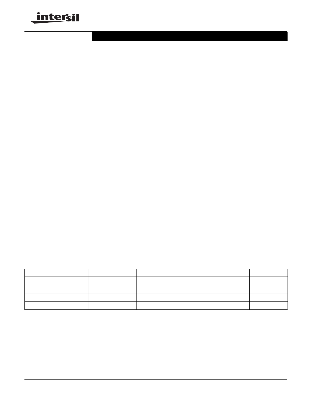
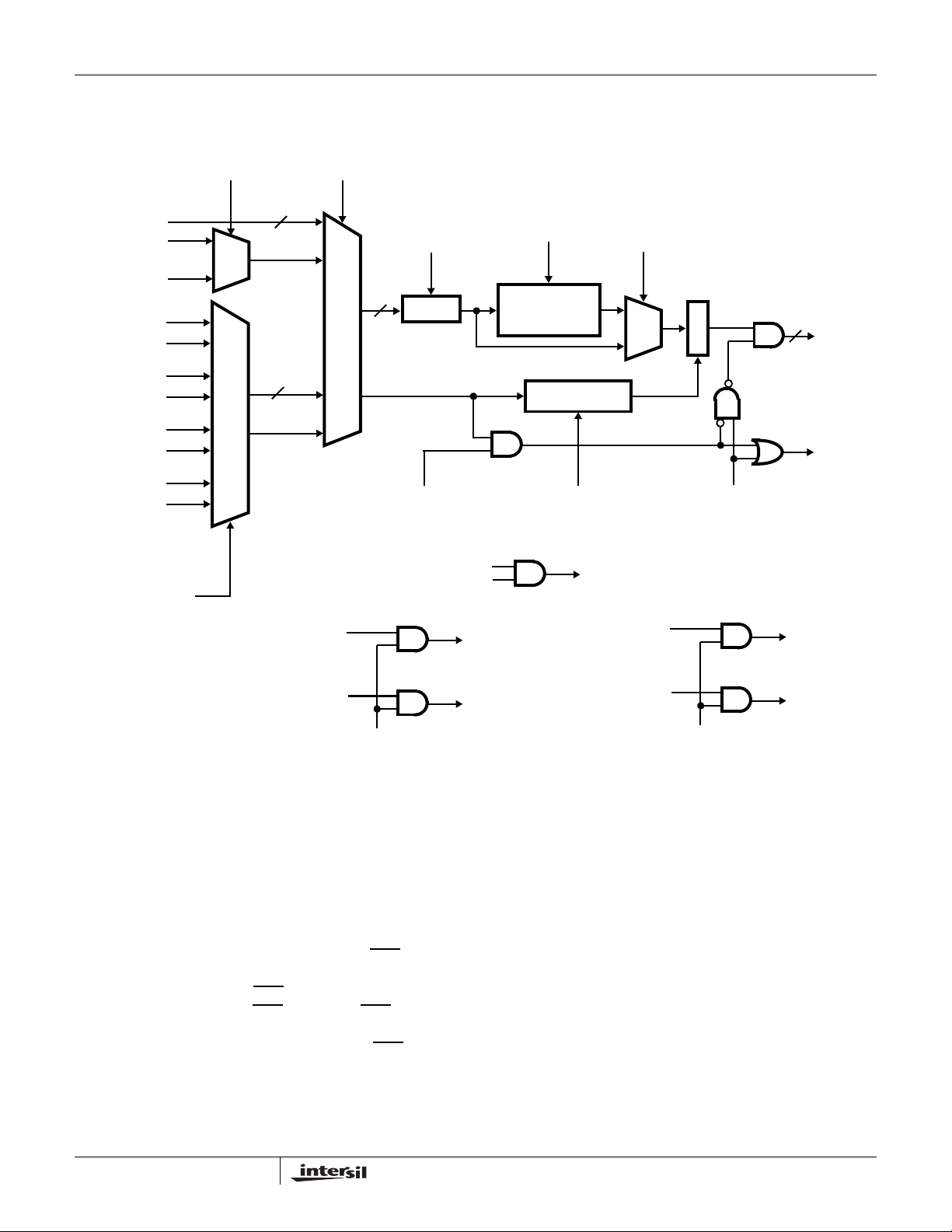
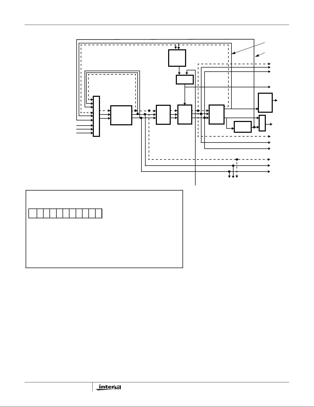
Block Diagram
www.BDTIC.com/Intersil
μP
TEST
REGISTER
INPUT SELECT,
FORMAT,
DEMUX
ISL5216
LEVEL
DETECTOR
SCLK
A(15:-1)
ENIA
B(15:-1)
ENIB
C(15:-1)
ENIC
D(15:-1)
ENID
INPUT SELECT,
FORMAT,
DEMUX
INPUT SELECT,
FORMAT,
DEMUX
INPUT SELECT,
FORMAT,
DEMUX
INPUT SELECT,
FORMAT,
DEMUX
NCO/MIXER/CIC
CHANNEL 0
NCO/MIXER/CIC
CHANNEL 1
NCO/MIXER/CIC
CHANNEL 2
NCO/MIXER/CIC
CHANNEL 3
I
Q
I
Q
I
Q
I
Q
BUS
ROUTING
FIR FILTERS,
AGC,
CARTESIAN-TO-POLAR
COORDINATE
CONVERTER
FIR FILTERS,
AGC,
CARTESIAN-TO-POLAR
COORDINATE
CONVERTER
FIR FILTERS,
AGC,
CARTESIAN-TO-POLAR
COORDINATE
CONVERTER
FIR FILTERS,
AGC,
CARTESIAN-TO-POLAR
COORDINATE
CONVERTER
SYNCA
SD1A
SD2A
SYNCB
SD1B
SD2B
OUTPUT
SELECT,
FORMAT,
SERIALIZE
SYNCC
SD1C
SD2C
SYNCD
SD1D
SD2D
CLK
RESET
SYNCI
SYNCO
SYNCI0
SYNCI1
SYNCI2
SYNCI3
TRST
TCLK
TMS
TDI
TDO
P(15:0) ADD(2:0) WR
μP INTERFACE
RD
or
RD/WR
DSTRB
2
INTRPT
or
μP MODE
CE
FN6013.3
July 13, 2007
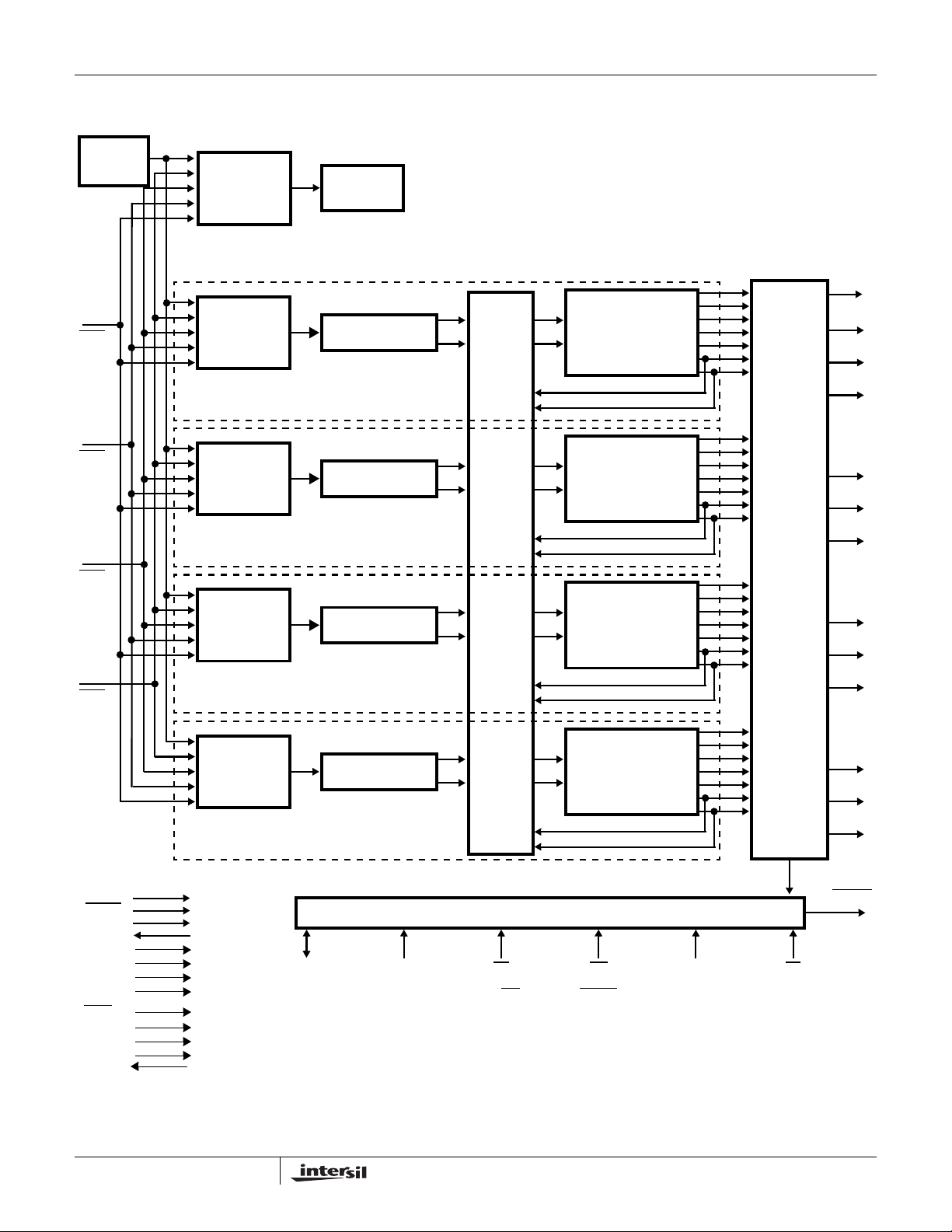
Pinout
www.BDTIC.com/Intersil
ISL5216
196 LD BGA
TOP VIEW
123456789 1110
A
A5
B
A3
A6
A8
C
A1
A2
A4
D
B14
A0 P13RESET
B15 P12
E
B13 P10GND
F
B11 GND P8VCC1
G
B9 VCC1 P6GND
H
CLK
VCC2
J
B7P2GND
K
B5 GND P0VCC1
L
B3 WR
M
B1
N
C15
P
B12
ENIB
B2
B0
C12C6C4C2C0
C14 C10 C8 GND VCC1 GND
A10 GNDVCC1
Am1 TDO
TMS
B10
TCLK
GND
TRST
B8
B6
B4 P1
Bm1
VCC1
SD1B
SYNCI3
TDI Cm1 Dm1
D15 D3D1D0
VCC1
ENIC
D13
SCLK SYNCCSYNCBSYNCA SYNCD SYNCI SYNCOA7 A9 A11 A13 A15 SD1A
SD1CGNDVCC2GND ADD0
SD2C SD2DSD2B
ADD2
SYNCI2
SYNCI1
SYNCI0
μP MODE
D11 ENID
VCC2 D9GND
D12 D10D14C13
12
SD1D
INTRPT
P9
P7
P5
D7
D8 D6 D4C11C9C7C5C3C1
13 14
ADD1
P15ENIA A12 A14 SD2A
VCC2P11
GND P4
VCC1P3
RDCE
D5 D2
P14
POWER PIN
GROUND PIN
VCC1 = +2.5V CORE SUPPLY VOLTAGE
VCC2 = +3.3V I/O SUPPLY VOLTAGE
SIGNAL PIN
THERMAL BALL
NC (NO CONNECTION)
3
FN6013.3
July 13, 2007

ISL5216
www.BDTIC.com/Intersil
Pin Descriptions
NAME TYPE DESCRIPTION
POWER SUPPLY
VCC1 - Positive Power Supply Voltage (core), 2.5V ±0.125
VCC2 - Positive Power Supply Voltage (I/O), 3.3V ±0.165
GND - Ground, 0V.
INPUTS
A(15:0), Am1 I Parallel Data Input bus A. Sampled on the rising edge of clock when ENIA
B(15:0), Bm1 I Parallel Data Input bus B. Sampled on the rising edge of clock when ENIB
C(15:0), Cm1 I Parallel Data Input bus C. Sampled on the rising edge of clock when ENIC
D15 I Parallel Data Input D15 or tuner channel 0 COF.
D14 I Parallel Data Input D14 or tuner channel 0 COFSync.
D13 I Parallel Data Input D13 or tuner channel 0 SOF.
D12 I Parallel Data Input D12 or tuner channel 0 SOFSync.
D11 I Parallel Data Input D11 or tuner channel 1 COF.
D10 I Parallel Data Input D10 or tuner channel 1 COFSync.
D9 I Parallel Data Input D9 or tuner channel 1 SOF.
D8 I Parallel Data Input D8 or tuner channel 1 SOFSync.
D7 I Parallel Data Input D7 or tuner channel 2 COF.
D6 I Parallel Data Input D6 or tuner channel 2 COFSync.
D5 I Parallel Data Input D5 or tuner channel 2 SOF.
D4 I Parallel Data Input D4 or tuner channel 2 SOFSync.
D3 I Parallel Data Input D3 or tuner channel 3 COF.
D2 I Parallel Data Input D2 or tuner channel 3 COFSync.
D1 I Parallel Data Input D1 or tuner channel 3 SOF.
D0 I Parallel Data Input D0 or tuner channel 3 SOFSync.
Dm1 I Parallel Data Input Dm1 for extended floating point input modes. Dm1 has internal weak pull-down.
ENIA
ENIB
ENIC
ENID
CONTROL
CLK I Input clock. All processing in the ISL5216 occurs on the rising edge of CLK.
SYNCI I Global synchronization input signal. Used to align the processing with an external event or with other ISL5216
SYNCI0 I Synchronization input signal for channel 0. Same functions as SYNCI but connects only to channel 0. This pin
SYNCI1 I Synchronization input signal for channel 1. Same functions as SYNCI but connects only to channel 1. This pin
SYNCI2 I Synchronization input signal for channel 2. Same functions as SYNCI but connects only to channel 2. This pin
I Input enable for Parallel Data Input bus A. Active low. This pin enables the input to the part in one of two modes,
I Input enable for Parallel Data Input bus B. Active low. This pin enables the input to the part in one of two modes,
I Input enable for Parallel Data Input bus C. Active low. This pin enables the input to the part in one of two
I Input enable for Parallel Data Input bus D. Active low. This pin enables the input to the part in one of two
weak pull-down.
weak pull-down.
weak pull-down.
gated or interpolated. In gated mode, one sample is taken per CLK when ENI
gated or interpolated. In gated mode, one sample is taken per CLK when ENI
modes, gated or interpolated. In gated mode, one sample is taken per CLK when ENI
modes, gated or interpolated. In gated mode, one sample is taken per CLK when ENI
or HSP50216 devices. SYNCI can update the carrier NCO, reset decimation counters, restart the filter
compute engine, and restart the output section among other functions. For most of the functional blocks, the
response to SYNCI is programmable and can be enabled or disabled. This signal is connected to all four
channels and is included for backward compatibility with HSP50216 designs.
is internally pulled low to allow it to be left unconnected.
is internally pulled low to allow it to be left unconnected.
is internally pulled low to allow it to be left unconnected.
is active (low). Am1 has internal
is active (low). Bm1 has internal
is active (low). Cm1 has internal
is asserted.
is asserted.
is asserted.
is asserted.
4
FN6013.3
July 13, 2007

ISL5216
www.BDTIC.com/Intersil
Pin Descriptions (Continued)
NAME TYPE DESCRIPTION
SYNCI3 I Synchronization input signal for channel 3. Same functions as SYNCI but connects only to channel 3. This pin
SYNCO O Synchronization Output Signal. The processing of multiple ISL5216 or HSP50216 devices can be
RESET
JTAG
TDO O Test data out
TDI I Test data in. Contains weak internal pull-up.
TMS I Test mode select. Contains weak internal pull-up.
TCLK I Test clock. Contains weak internal pull-down.
TRST
OUTPUTS
SD1A O Serial Data Output 1A. A serial data stream output which can be programmed to consist of I1, Q1, I2, Q2,
SD2A O Serial Data Output 2A. This output is provided as an auxiliary output for Serial Data Output 1A to route data to
SD1B O Serial Data Output 1B. See description for SD1A.
SD2B O Serial Data Output 2B. See description for SD2A.
SD1C O Serial Data Output 1C. See description for SD1A.
SD2C O Serial Data Output 2C. See description for SD2A.
SD1D O Serial Data Output 1D. See description for SD1A.
SD2D O Serial Data Output 2D. See description for SD2A.
SCLK O Serial Output Clock. Can be programmed to be at 1, 1/2, 1/4, 1/8, or 1/16 times the clock frequency. The
SYNCA O Serial Data Output 1A sync signal. This signal is used to indicate the start of a data word and/or frame of data.
SYNCB O Serial Data Output 1B sync signal. This signal is used to indicate the start of a data word and/or frame of data.
SYNCC O Serial Data Output 1C sync signal. This signal is used to indicate the start of a data word and/or frame of data.
SYNCD O Serial Data Output 1D sync signal. This signal is used to indicate the start of a data word and/or frame of data.
MICROPROCESSOR INTERFACE
P(15:0) I/O Microprocessor Interface Data bus. See Microprocessor Interface Section. P15 is the MSB.
ADD(2:0) I Microprocessor Interface Address bus. ADD2 is the MSB. See Microprocessor Interface Section. Note: ADD2
WR
or
DSTRB
I Reset Signal. Active low. Asserting reset will halt all processing and set certain registers to default values.
I Test reset. Active low. Contains weak internal pull-down.
I Microprocessor Interface Write or Data Strobe Signal. When the Microprocessor Interface Mode Control, μP
is internally pulled low to allow it to be left unconnected.
synchronized by tying the SYNCO from one ISL5216 device (the master) to the SYNCI of all the
ISL5216/HSP50216 devices (the master and slaves).
magnitude, phase, frequency (dφ/dt), AGC gain, and/or zeros. In addition, data outputs from Channels 0, 1, 2
and 3 can be multiplexed into a common serial output data stream. Information can be sequenced in a
programmable order. See Serial Data Output Formatter Section and Microprocessor Interface Section.
a second destination or to output two words at a time for higher sample rates. SD2A has the same
programmability as SD1A except that floating point format is not available. See Serial Data Output Formatter
Section and Microprocessor Interface Section.
polarity of SCLK is programmable.
The polarity and position of SYNCA is programmable.
The polarity and position of SYNCB is programmable.
The polarity and position of SYNCC is programmable.
The polarity and position of SYNCD is programmable.
is not used but designated for future expansion.
MODE, is a low data transfers (from either P(15:0) to the internal write holding register or from the internal write
holding register to the target register specified) occur on the low to high transition of WR
(low). When the μP MODE control is high this input functions as a data read/write strobe. In this mode with
low data transfers (from either P(15:0) to the internal write holding register or from the internal write
RD/WR
holding register to the target register specified) occur on the low to high transition of Data Strobe. With RD/WR
high the data from the address specified is placed on P(15:0) when Data Strobe is low. See Microprocessor
Interface Section.
when CE is asserted
5
FN6013.3
July 13, 2007
ISL5216
www.BDTIC.com/Intersil
Pin Descriptions (Continued)
NAME TYPE DESCRIPTION
RD
or
RD/WR
μP MODE I Microprocessor Interface Mode Control. This pin is used to select the Read/Write mode for the Microprocessor
CE
INTRPT
I Microprocessor Interface Read or Read/Write Signal. When the Microprocessor Interface Mode Control, μP
I Microprocessor Interface Chip Select. Active low. This pin has the same timing as the address pins.
O Microprocessor Interrupt Signal. Asserted for a programmable number of clock cycles when new data is
MODE, is a lo w the data from the address specified is placed on P(15:0) when RD
is asserted (low). When the μP MODE control is high this input functions as a Read/Write
is read from P(15:0) when high or written to the appropriate register when low. See Microprocessor Interface
Section.
Interface. Internally pulled down. See Microprocessor Interface Section.
available on the selected Channel.
is asserted (low) and CE
control input. Data
Functional Description
The ISL5216 is a 4-channel digital receiver integrated circuit
offering exceptional dynamic range and flexibility. Each of
the four channels consists of a front-end NCO, digital mixer,
and CIC-filter block and a back-end FIR, AGC and Cartesian
to polar coordinate-conversion block. The parameters for the
four channels are independently programmable. Four 17-bit
parallel data input busses (A(15:-1), B(15:-1), C(15:-1) and
D(15:-1)) and four pairs of serial data outputs (SDxA, SDxB,
SDxC, and SDxD; x = 1 or 2) are provided. Each input can
be connected to any or all of the internal signal processing
channels, Channels 0, 1, 2 and 3. The output of each
channel can be routed to any of the serial outputs. Outputs
from more than one channel can be multiplexed through a
common output if the channels are synchronized. The four
channels share a common input clock and a common serial
output clock, but the output sample rates can be
synchronous or asynchronous. Bus multiplexers between
the front end and back end sections provide flexible routing
between channels for cascading back-end filters or for
routing one front end to multiple back ends for polyphase
filtering or systolic arrays (to provide wider bandwidth
filtering). A level detector is provided to monitor the signal
level on any of the parallel data input busses, facilitating
microprocessor control of gain blocks prior to an A/D
converter.
Each front end NCO/digital mixer/CIC filter section includes
a quadrature numerically controlled oscillator (NCO), digital
mixer, barrel shifter and a cascaded-integrator-comb filter
(CIC). The NCO has a 32-bit frequency control word for
22.1mHz tuning resolution at an input sample rate of
95MSPS. The SFDR of the NCO is >115dB. The CIC filter
order is programmable between 1 and 5 and the CIC
decimation factor can be programmed from 4 to 512 for 5
order, 2048 for 4
st
1
or 2nd order filters.
th
order, 32768 for 3rd order, or 65536 for
th
Each channel back end section includes an FIR processing
block, an AGC and a cartesian-to-polar coordinate
converter. The FIR processing block is a flexible filter
compute engine that can compute a single FIR or a set of
cascaded decimating, interpolating or resampling filters. A
single filter in a chain can have up to 256 taps and the total
number of taps in a set of filters can be up to 384 provided
that the decimation is sufficient. The ISL5216 calculates two
taps per clock (on each channel) for symmetric filters,
generally making decimation the limiting factor for the
number of taps available. The filter compute engine supports
a variety of filter types including decimation, interpolation
and resampling filters. The coefficients for the programmable
digital filters are 22 bits wide. Coefficients are provided in
ROM for several halfband filter responses and for a
resampler. The AGC section can provide up to 96dB of
either fixed or automatic gain control. For automatic gain
control, two settling modes and two sets of loop gains are
provided. Separate attack and decay slew rates are provided
for each loop gain. Programmable limi ts allow the user to
select a gain range less than 96dB. The outputs of the
cartesian-to-polar coordinate conversion block, used by the
AGC loop, are also provided as outputs to the user for AM
and FM demodulation.
The ISL5216 supports both fixed and floating point parallel
data input modes. The floating point modes support gain
ranging A/D converters. Gated, interpolated and multiplexed
data input modes are supported. The serial data output word
width for each data type can be programmed to one of ten
output bit widths from 4-bit fixed point through 32-bit IEEE
754 floating point.
The ISL5216 is programmed through a 16-bit
microprocessor interface. The output data can also be read
via the microprocessor interface for all channels that are
synchronized. The ISL5216 is specified to operate to a
maximum clock rate of 95MSPS over the industrial
temperature range (-40°C to 85°C). The I/O power supply
voltage range is 3.3V ± 0.165V while the core power supply
voltage is 2.5V ± 0.125V. The I/Os are 5V tolerant.
6
FN6013.3
July 13, 2007
Input Select/Format Block
www.BDTIC.com/Intersil
ISL5216
(IWA *000 - 12
or GWA F804 - 12)
μP TEST
REGISTER
(GWA F807 - 15:0)
TESTENBIT
(IWA *000 - 11
or GWA F804 - 11)
TESTENSTRB
(GWA F808)
A(15:-1)
ENIA
B(15:-1)
ENIB
C(15:-1)
ENIC
D(15:-1)
ENID
NOTE: ENI* SIGNALS
ARE ACTIVE HIGH
(INVERTED AT THE I/O PAD)
EXTERNAL DATA
INPUT SELECT
(IWA *000 - 14:13
or
GWA F804 - 14:13)
TEST ENI
SELECT
TESTEN
MUX
MUX
CARRIER OFFSET
FREQUENCY (COF)
EXTERNAL/TEST
SELECT
(IWA *000 - 15
or GWA F804 - 15)
15:0
15:0
ENI
OFFSET BINARY
OR
TWO’s COMPLEMENT
(IWA *000 - 10
or GWA F804 - 10)
15:0
FORMAT
MUX
EN
INPUT ENABLE HOLD OFF
(ENABLED BY SYNCI)
(GWA F802 - 30)
ENABLE PN
(IWA *000 - 0)
COF TO
CARRIER
NCO/MIXER
11/3, 12/3, 13/3
14/2, 14/3, 15/2, 16/1
(IWA *000 or
GWA F804 - 17:16, 8:7)
FLOATING POINT
TO
FIXED POINT
PROGRAMMABLE
DE-MULTIPLEX
CONTROL (0-7)
(IWA *000 - 6:4
or GWA F8O4 - 6:4)
PN
OFFSET FREQUENCY
DELAY
PN TO
CARRIER
NCO/MIXER
FIXED POINT
FLOATING POINT
(IWA *000 - 9
or GWA F804 - 9)
MUX
RESAMPLER
(SOF)
OR
R
E
G
INTERPOLATED/GATED
MODE
(IWA *000 - 3
or GWA F804 - 3)
15:0
DATA
TO
NCO/MIXER
OR
LEVEL
DETECTOR
DATA
SAMPLE
ENABLE
SOF TO
RESAMPLER
NCO
COF SYNC
ENABLE
COF
(1WA *000 - 2)
Each front end block and the level detector block contains an
input select/format block. A functional block diagram is
provided in the above figure. The input source can be any of
the four parallel input busses (see Microprocessor Interface
Section Table 1, IWA *000h) or a test register loaded via the
processor bus (see Microprocessor Interface Section, GWA
register F807h).
The input to the part can operate in a gated or interpolated
mode. Each input data bus has an input enable (ENIx
,x=A,
B, C or D). In the gated mode, one input sample is
processed per clock that the ENIx
Processing is disabled when ENIx
signal is asserted (low).
is high. The ENIx signal is
pipelined through the part to minimize delay (latency). In the
interpolated mode, the input is zeroed when the ENIx
signal
is high, but processing inside the part continues. This mode
inserts zeros between the data samples, interpolating the
input data stream up to the clock rate. On reset, the part is
set to gated mode and the input enables are disabled. The
COF SYNC TO
CARRIER
NCO/MIXER
SOF SYNC
ENABLE
SOF
(IWA *000 - 1)
inputs are enabled by the first global SYNCI signal or
SYNCIx signal, where X = 0, 1, 2 or 3.
The input section can select one channel from a multiplexed
data stream of up to eight channels. The input enable is
delayed by zero to seven clock cycles to enable a selection
register . Th e re gi ster following the selection register is
enabled by the non-delayed input enable to realign the
processing of the channels. The one-clock-wide input enable
must align with the data for the first channel. The desired
channel is then selected by programming the delay. A delay
of zero selects the first channel, a delay of one selects the
second, etc.
The parallel input busses are 17 bits wide allowing for up to 16
bits of fixed-point data or 14 bits of mantissa with three bit s of
exponent for floating-point data. The input format may be twos
complement or offset binary format in either fixed or floating
SOF SYNC TO
RESAMPLER
NCO
7
FN6013.3
July 13, 2007
ISL5216
www.BDTIC.com/Intersil
point modes. The floating point modes and the mapping of the
parallel 17-bit input format is discussed below.
as those which follow it in the tables below use the CIC’s
barrel shifter to provide the gain. This places a limit on the
CIC’s largest available decimation. As an example, assume
Floating Point Input Mode Bit Mapping
The input bit weighting for fixed point inputs on busses A, B,
C, and D is:
bit 15 (MSB): 2
0
, bit 14: 2-1, bit 13: 2-2, ..., bit 0: 2
For floating point modes, the least significant two or three
bits are used as exponent bits (See Floating Point Input
Mode Bit Mapping Tables).
The first three floating point modes shown below are included
for backward compatibility with the HSP50216 and th eir
functionality remains unchanged. The 14-bit mantissa/2-bit
exponent mode present in the HSP50216 has been extended
-15
.
the CIC is set for 5th order and the decimation needs to be
300. The CIC’s gain, 300
shifter with a shift factor of 45 - ceil(log
5
, is compensated for in the barrel
(3005)) = 3 where
2
shifts are from LSB towards MSB and a shift of 45
corresponds to no attenuation. If the shift factor is set as 0 in
this example, there is room for 3 * 6 = 18dB of gain. Raising
the CIC decimation lowers the shift factor (to further attenuate
the CIC input signal) and limits the available gain range. This
CIC decimation/floating point gain range trade off is hand led
automatically by the evaluation board software. Additi onal
information on the CIC can be found in the CIC Filter section
of this data sheet.
from a 12dB range to 18dB in the ISL5216. This mode as well
Floating Point Input Mode Bit Mapping Tables
((
EXPONENT GAIN (dB) PIN BIT WEIGHTING TO 16-BIT INPUT MAPPING
X(2:0) = 000 0 X15 X15 X15 X15 X15 X15 X14 X13 X12 X11 X10 X9 X8 X7 X6 X5
X(2:0) = 001 6 X15 X15 X15 X15 X15 X14 X13 X12 X11 X10 X9 X8 X7 X6 X5 X4
X(2:0) = 010 12 X15 X15 X15 X15 X14 X13 X12 X11 X10 X9 X8 X7 X6 X5 X4 X3
X(2:0) = 011 18 X15 X15 X15 X14 X13 X12 X11 X10 X9 X8 X7 X6 X5 X4 X3 0
X(2:0) = 100 24 X15 X15 X14 X13 X12 X11 X10 X9 X8 X7 X6 X5 X4 X3 0 0
X(2:0) = 101
(Note 1)
NOTES:
1. Or 110 or 111, the exponent input saturates at 101.
2. “Xnn” = input A, B, C, or D bit nn.
3. To select this mode, set IWA *000H/GWA F804H bits 17, 16, 8 and 7 to 0.
11-BIT MODE: 11 TO 13-BIT MANTISSA (15:3), 3-BIT EXPONENT (2:0), 30dB EXPONENT RANGE (Note 3)
30 X15 X14 X13 X12 X11 X10 X9 X8 X7 X6 X5 X4 X3 0 0 0
12-BIT MODE: 12 TO 13-BIT MANTISSA (15:3), 3-BIT EXPONENT (2:0), 24dB EXPONENT RANGE (Note 5)
EXPONENT GAIN (dB) PIN BIT WEIGHTING TO 16-BIT INPUT MAPPING
X(2:0) = 000 0 X15 X15 X15 X15 X15 X14 X13 X12 X11 X10 X9 X8 X7 X6 X5 X4
X(2:0) = 001 6 X15 X15 X15 X15 X14 X13 X12 X11 X10 X9 X8 X7 X6 X5 X4 X3
X(2:0) = 010 12 X15 X15 X15 X14 X13 X12 X11 X10 X9 X8 X7 X6 X5 X4 X3 0
X(2:0) = 011 18 X15 X15 X14 X13 X12 X11 X10 X9 X8 X7 X6 X5 X4 X3 0 0
X(2:0) = 100
(Note 4)
NOTES:
4. Or 101, 110, or 111, the exponent input saturates at 100.
5. To select this mode, set IWA *000H/GWA F804H bits 17, 16, 8 and 7 to 0, 0, 0 and 1 respectively.
24 X15 X14 X13 X12 X11 X10 X9 X8 X7 X6 X5 X4 X3 0 0 0
8
FN6013.3
July 13, 2007
ISL5216
www.BDTIC.com/Intersil
13-BIT MODE: 13-BIT MANTISSA (15:3), 3-BIT EXPONENT (2:0), 18dB EXPONENT RANGE (Note 7)
EXPONENT GAIN (dB) PIN BIT WEIGHTING TO 16-BIT INPUT MAPPING
X(2:0) = 000 0 X15 X15 X15 X15 X14 X13 X12 X11 X10 X9 X8 X7 X6 X5 X4 X3
X(2:0) = 001 6 X15 X15 X15 X14 X13 X12 X11 X10 X9 X8 X7 X6 X5 X4 X3 0
X(2:0) = 010 12 X15 X15 X14 X13 X12 X11 X10 X9 X8 X7 X6 X5 X4 X3 0 0
X(2:0) = 011
(Note 6)
NOTES:
6. Or 100, 101, 110, or 111, the exponent input saturates at 011.
7. To select this mode, set IWA *000H/GWA F804H bits 17, 16, 8 and 7 to 0, 0, 1 and 0 respectively.
EXPONENT GAIN (dB) PIN BIT WEIGHTING TO 16-BIT INPUT MAPPING
X(1:0) = 00 0 X15 X14 X13 X12 X11 X10 X9 X8 X7X6X5X4X3X2 0 0
X(1:0) = 01 6 X15 X14 X13 X12 X11 X10 X9 X8 X7X6X5X4X3X2 0 0
X(1:0) = 10 12 X15 X14 X13 X12 X11 X10 X9 X8 X7 X6 X5 X4 X3 X2 0 0
X(1:0) = 11 18 X15 X14 X13 X12 X11 X10 X9 X8 X7 X6 X5 X4 X3 X2 0 0
NOTE:
8. To select this mode, set IWA *000H/GWA F804H bits 17, 16, 8 and 7 to 0, 0, 1 and 1 respectively.
EXPONENT GAIN (dB) PIN BIT WEIGHTING TO 16-BIT INPUT MAPPING
X(-1,1,0) = 0000 X15 X14 X13 X12 X11 X10 X9 X8 X7X6X5X4X3X2 0 0
X(-1,1,0) = 0016 X15 X14 X13 X12 X11 X10 X9 X8 X7X6X5X4X3X2 0 0
X(-1,1,0) = 010 12 X15 X14 X13 X12 X11 X10 X9 X8 X7 X6 X5 X4 X3 X2 0 0
X(-1,1,0) = 011 18 X15 X14 X13 X12 X11 X10 X9 X8 X7X6X5X4X3X2 0 0
X(-1,1,0) = 100 24 X15 X14 X13 X12 X11 X10 X9 X8 X7 X6 X5 X4 X3 X2 0 0
X(-1,1,0) = 101 30 X15 X14 X13 X12 X11 X10 X9 X8 X7 X6 X5 X4 X3 X2 0 0
X(-1,1,0) = 110 36 X15 X14 X13 X12 X11 X10 X9 X8 X7X6X5X4X3X2 0 0
X(-1,1,0) = 111 42 X15 X14 X13 X12 X11 X10 X9 X8 X7X6X5X4X3X2 0 0
NOTE:
9. To select this mode, set IWA *000H/GWA F804H bits 17, 16, 8 and 7 to 1, 0, 1 and 1 respectively.
18 X15 X14 X13 X12 X11 X10 X9 X8 X7 X6 X5 X4 X3 0 0 0
14-BIT MODE: 14-BIT MANTISSA (15:2), 2-BIT EXPONENT (1:0), 18dB MAXIMUM EXPONENT RANGE (Note 8)
14-BIT MODE: 14-BIT MANTISSA (15:2), 3-BIT EXPONENT (-1,1,0), 42dB MAXIMUM EXPONENT RANGE (Note 9)
11, 12, 13-BIT MODE: 11, 12, 13-BIT MANTISSA, 3-BIT EXPONENT (-1,1,0) (Note 10), 42dB MAXIMUM EXPONENT RANGE (Note 11)
EXPONENT GAIN (dB) PIN BIT WEIGHTING TO 16-BIT INPUT MAPPING
X(-1,1,0) = 0000 X15 X14 X13 X12 X11 X10 X9 X8 X7X6X5X4X3 0 0 0
X(-1,1,0) = 0016 X15 X14 X13 X12 X11 X10 X9 X8 X7X6X5X4X3 0 0 0
X(-1,1,0) = 010 12 X15 X14 X13 X12 X11 X10 X9 X8 X7 X6 X5 X4 X3 0 0 0
X(-1,1,0) = 011 18 X15 X14 X13 X12 X11 X10 X9 X8 X7X6X5X4X3 0 0 0
X(-1,1,0) = 100 24 X15 X14 X13 X12 X11 X10 X9 X8 X7 X6 X5 X4 X3 0 0 0
X(-1,1,0) = 101 30 X15 X14 X13 X12 X11 X10 X9 X8 X7 X6 X5 X4 X3 0 0 0
X(-1,1,0) = 110 36 X15 X14 X13 X12 X11 X10 X9 X8 X7X6X5X4X3 0 0 0
X(-1,1,0) = 111 42 X15 X14 X13 X12 X11 X10 X9 X8 X7X6X5X4X3 0 0 0
NOTES:
10. For compatibility with legacy HSP50216 11, 12 and 13 bit floating point modes as well as the new ISL5216 modes, the most significant exponent
bit is taken as X2 OR’d with X-1. Either input may be used for the MSB of the exponent when the other is tied low.
11. T o select these modes, set IW A *000H/GWA F804H bits 17 and 16 to 1 and 0, respectively , and bit s 8 and 7 to 0 and 0 for 1 1/3, 0 and 1 for 12/3,
and 1 and 0 for 13/3.
9
FN6013.3
July 13, 2007
ISL5216
www.BDTIC.com/Intersil
15-BIT MODE: 15-BIT MANTISSA (15:1), 2-BIT EXPONENT (-1, 0), 18dB MAXIMUM EXPONENT RANGE (Note 12)
EXPONENT GAIN (dB) PIN BIT WEIGHTING TO 16-BIT INPUT MAPPING
000 0 X15 X14 X13 X12 X11 X10 X9 X8 X7X6X5X4X3X2X1 0
001 6 X15 X14 X13 X12 X11 X10 X9 X8 X7X6X5X4X3X2X1 0
010 12 X15 X14 X13 X12 X11 X10 X9 X8 X7 X6 X5 X4 X3 X2 X1 0
011 18 X15 X14 X13 X12 X11 X10 X9 X8 X7X6X5X4X3X2X1 0
NOTE:
12. To select this mode, set IWA *000H/GWA F804H bits 17, 16, 8 and 7 to 1, 1, 0 and 0 respectively.
16-BIT MODE: 16-BIT MANTISSA (15:0), 1-BIT EXPONENT (-1), 6dB MAXIMUM EXPONENT RANGE (Note 13)
EXPONENT GAIN (dB) PIN BIT WEIGHTING TO 16-BIT INPUT MAPPING
X(-1) = 0 0 X15 X14 X13 X12 X11 X10 X9 X8 X7 X6 X5 X4 X3 X2 X1 X0
X(-1) = 1 6 X15 X14 X13 X12 X11 X10 X9 X8 X7 X6 X5 X4 X3 X2 X1 X0
NOTE:
13. To select this mode, set IWA *000H/GWA F804H bits 17, 16, 8 and 7 to 1, 1, 0 and 1 respectively.
Level Detector
An input level detector is provided to monitor the signal level
on any of the input busses. The input bus, input format, and
the level detection type are programmable (see
Microprocessor Interface , GWA registers F804h, F805h and
F806h). This signal level represents the wideband signal from
the A/D and is useful for controlling gain/attenuation blocks
ahead of the converter.
The supported monitoring modes include integrated
magnitude (like the HSP50214 w/o the threshold) and leaky
integration (Y
-16
or 2
(see GWA = F805h). The measurement interval can
n=Xn
xA+Y
x (1-A)) where A = 1, 2-8, 2
n-1
be programmed from 2 to 65537 samples (or continuous for
the leaky integrator case). The output is 32 bits and is read via
the μP interface.
Note that the accumulators in the input level detector are 32
bits wide. This may limit the integration range to as few as
512 samples (for a 42dB exponent range).
ABSOLUTE
VALUE
-12
EN
A
16
0, -8, -12, -16
,
2
FIGURE 2. PEAK DETECTOR (See “Errata” on page 63)
16
X
B
BARREL SHIFTER
MODE NOT
BARREL SHIFTER
A > B
Σ
PPORTED
SU
EN
R
E
G
YN = A * X + (1 - A) * Y
R
E
Σ
G
32
N-1
Y
32
MSB
16
FIGURE 1. INTEGRATED MODE
BARREL SHIFTER
0, -8, -12, -16
2
ACCUMULATOR
32
0, -8, -12, -16
2
A =
10
BARREL SHIFTER
FIGURE 3. LEAKY INTEGRATOR
FN6013.3
July 13, 2007

ISL5216
www.BDTIC.com/Intersil
Complex Input Mode
In this mode, complex (I/Q) data can be input using two clock
cycles with I input first and Q input second. The ENIx
indicates the clock cycle when I is valid. The Q data is taken
on either the next input clock or two clocks after I, as
determined by IWA *000H bit 23. The complex multiply is
done in two clock cycles: I * COS and I * SIN on the first
clock and Q * (-SIN) and Q * COS on the second clock cycle.
The first integrator of the CIC is enabled on both clock cycles
to add the two products. The rest of the stages are enabled
only on the first cycle.
In complex input mode, the input level detector uses only I
samples for its magnitude computation.
The CIC decimation counter is programmed for two times
the number of complex input samples. The exponent input
must be the same for I and Q for the floating point modes.
See IWA *000h for details on controlling the complex input
mode.
signal
NCO/Mixer
After the input select/format section, the samples are
multiplied by quadrature sine wave samples from the carrier
NCO. The NCO has a 32-bit frequency control, providing
sub-hertz resolution at the maximum clock rate. The
quadrature sinusoids have exceptional purity. The purity of
the NCO should not be the determining factor for the
receiver dynamic range performance. The phase
quantization to the sine/cosine generator is 24 bits and the
amplitude quantization is 19 bits.
The carrier NCO center frequency is loaded via the μP bus.
The center frequency control is double buffered - the input
is loaded into a center frequency holding register via the μP
interface. The data is then transferred from the holding
register to the active register by a write to a address IWA
*006h or by a SYNCI signal, if loading via SYNCI is
enabled. To synchronize multiple channels, the carrier
NCO phase accumulator feedback can be zeroed on
loading to restart all of the NCOs at the same phase. A
serial offset frequency input is also available for each
channel through the D(15:0) parallel data input bus (if that
bus is not needed for data input). This is legacy support for
HSP50210 type tracking signals. See IWA=*000 and *004
for carrier offset frequency parameters.
After the mixers, a PN (pseudo noise) signal can be added to
the data. This feature is provided for test and to digitally
reduce the input sensitivity and adjust the receiver range
(sensitivity). The effect is th e same as increasing the noise
figure of the receiver, reducing its sensitivity and overall
dynamic range. For testing, the PN generator provides a
wideband signal which may be used to verify the frequency
response of a filter. The one bit PN dat a is scale d by a 16-bit
programmable scale factor. The overall range for the PN is 0
to 1/4 full scale (see IWA = *001h). A gain of 0 disables the
PN input. The PN value is formed as:
PN VALUE
-32-4............2-172-18
2
SSS X X XXXXXXXXXXXX X X
where S is the sign extension of the 16 bit PN gain register
value (IWA = *001H) times the PN chip value and the 16 X’s
refer to the PN gain register times the PN chip value.
The minimum, non-zero, PN value is 2
(-108dBFS) on each axis (-105dBFS total). For an input noise
level of -75dBFS, this allows the SNR to be decreased in
steps of 1/8dB or less. The I and Q PN codes are offset in ti me
to decorrelate them. The PN code is selected and enabled in
the test control register (F800h). The PN is added to the signal
after the mix with the three sign bits aligned with the most
significant three bits of the signal, so the maximum level is 12dBFS and the minimum, non-zero level is -108dBFS. The
PN code can be 2
15
-1, 223-1 or 215-1 * 223-1.
-18
of full scale
CIC Filter
Next, the signal is filtered by a cascaded integrator/comb
(CIC) filter. A CIC filter is an efficient architecture for
decimation filtering. The power or magnitude squared
frequency response of the CIC filter is given by:
πMf()sin
πf
⎛⎞
---- -
⎝⎠
R
2N
max
/4
⎛⎞
⎜⎟
------------------------
=
Pf()
⎜⎟
⎜⎟
sin
⎝⎠
where
M = Number of delays (1 for the ISL5216)
N = Number of stages
and R = Decimation factor.
The passband frequency response for first (N=1) though fifth
(N=5) order CIC filters is plotted in Figure 13. The frequency
axis is normalized to f
sample rate. Figure 15 shows the frequency response for a
th
5
order filter but extends the frequency axis to fS/R = 3
(3 times the CIC output sample rate) to show alias rejection
for the out of band signals. Figure 14 uses information from
Figure 15 to provide the amplitude of the first (strongest)
alias as a function of the signal frequency or bandwidth from
DC. For example, with a 5
(signal frequency is 1/8 the CIC output rate) Figure 14 shows
a first alias level of about -87 dB. Figure 14 is also listed in
table form in Table 51 (CIC Passband and Alias Levels).
The CIC filter order is programmable from 0 to 5. The CIC
may be bypassed by setting the CIC filter order to 0
(IWA = *004h bits 13:9 are all set equal to 1) and the CIC
barrel shift (IWA = *004h bits 19:14) to 45 decimal. The CIC
output rate must, however, be no more than CLK
where CLK
the device (see electrical specifications section).
is the maximum clock frequency available on
max
/R, making fS/R = 1 the CIC output
S
th
order CIC and fS/R = 0.125
11
FN6013.3
July 13, 2007

The integrator bit widths are 69, 62, 53, 44, and 34 for the
www.BDTIC.com/Intersil
t
first
through fifth stages, respectively, while the comb bit
widths are all 32. The integrators are sized for decimation
factors of up to 512 with five stages, 2048 with fou r stages,
32768 with three stages, and 65536 with one o r two stages.
Higher decimations in the CIC should be avoided as they
will cause integrator overflow. In the ISL5216, the
integrators are slightly oversized to reduce the quantization
noise at each stage.
A CIC filter has a gain of R
and N is the number of stages. Because the CIC filter gain
can become very large with decimation, an attenuator is
provided ahead of the CIC to prevent overflow. The 24 bits of
sample data are placed on the low 24 bits of a 69 bit bus
(width of the first CIC integrator) for a gain of 2
barrel shifter then provides a gain of 2
before passing the data to the CIC. The overall gain in the
pre-CIC attenuator can therefore be programmed to be any
one of 48 values from 2
bits 19:14). This shift factor is adjusted to keep the total
barrel shifter and CIC filter gain between 0.5 and 1.0. The
equation which should be used to compute the necessary
shift factor is:
N
, where R is the decimation factor
-45
0
to 247 inclusive
-45
to 4, inclusive (see IWA=*004,
. A 48 bit
ISL5216
Shift Factor = 45 - Ceiling(log
CIC barrel shifts of greater than 45 will cause MSB bits to be
lost. Most of the floating point modes on the ISL5216 make
use of the CIC barrel shifter for gain. This limits the
maximum usable decimation. In particular, shift factor minus
maximum exponent must be greater than or equal to zero.
Maximum exponent ranges from 0 to 1, 3, or 7 for 1, 2 and 3
exponent bits, representing up to 6, 18, or 42dB of gain,
respectively. See F loating Point Input Mode section for
details.
(RN)).
2
12
FN6013.3
July 13, 2007
Back End Data Routing
www.BDTIC.com/Intersil
ISL5216
MAG: I
PATH 0
(4:0)
M
U
X
FROM
CIC
DESTINATION BIT MAP
(BITS 28:18 OF FIR INSTRUCTIONS BIT FIELD)
FILTER
COMPUTE
ENGINE
FIFO/
TIMER
PATH 2
AGC
LOOP
FILTER
MUX
AGC
MULT
EXT AGC
GAIN
PATH 1
PATH 3
CART
TO
POLAR
SHIFT
d/dt
x1, x2
x4, x8
M
U
X
dphi/dt: Q
I1
Q1
GAIN
MAG
PHASE
I2
Q2
I2
Q2
26
28 27 25 24 23 22 21 20 19 18
28
27
26, 25
24
23
22:18
AGC LOOP GAIN SELECT (PATH 01 ONLY)
UPDATE AGC LOOP (PATH 01 ONLY)
PATH 00 - - IMMEDIATE FILTER PROCESSOR FEEDBACK PATH
01 - - FIFO/AGC PATH TO I1 AND Q1
10 - - DIRECT OUT/CASCADE PATH TO I2 AND Q2
11 - - FIFO/AGC PATH TO I2 AND Q2
STROBE OUTPUT SECTION (START SERIAL OUTPUT WITH THIS SAMPLE)
FEED MAG/PHASE BACK TO FILTER PROCESSOR
FILTER PROCESSOR SEQUENCE STEP NUMBER
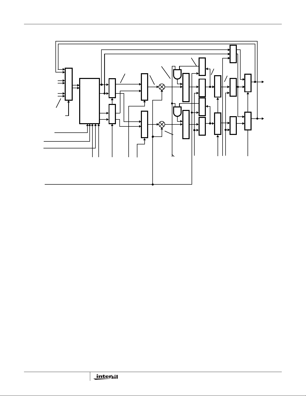
Back End Section
One back-end processing section is provided per channel.
Each back end section consists of a filter compute engine, a
FIFO/timer for evenly spacing samp l es (important when
implementing interpolation filters and resamplers), an AGC
and a cartesian-to-polar coordinate conversion block. A
block diagram showing the major functional blocks and data
routing is shown above. The data input to the back end
section is through the filter compute engine. There are two
other inputs to the filter compute engine, they are a data
recirculation path for cascading filters and a magnitude and
dφ/dt feedback path for AM and FM filtering. There are seven
outputs from each back end processing section. These are I
and Q directly out of the filter compute engine (I2, Q2), I and
Q passed through the FIFO and AGC multipliers (I1, Q1),
magnitude (MAG), phase (or dφ/dt), and the AGC gain
control value (GAIN). The I2/Q2 outputs are used when
cascading back end stages. The routing of signals within the
back end processing section is controlled by the filter
compute engine. The routing information is embedded in the
instruction bit fields used to define the digital filter being
implemented in the filter compute engine.
13
FN6013.3
July 13, 2007
Filter Compute Engine
www.BDTIC.com/Intersil
IQ
R/dφ/dt
0..-23
INMUX (1:0)
ADDRA (8:0)
ADDRB (8:0)
M
U
X
RAMR/Wb
WORDS
RAM
384
ISL5216
R
DOWN SHIFT
1..-25
WITH RND
0..-23
I
Q
I
Q
A
S
W
B
A
P
S
W
A
A
P
B
1..-23
A
L
U
A
L
U
0, 1, 2 PLACES
∑
∑
0..-21
S
H
9..-31
F
T
L
R
E
G
S
H
F
T
R
E
G
M
T
L
M
T
E
G
0..-23
I
I
I
I
M
U
R
X
E
G
M
U
R
X
E
G
IFUNCT
QFUNCT
COEF (21:0), SHIFT (1:0)
RAMAEN
RAMBEN
IQSWAP
The filter compute engine is a dual multiply-accumulator
(MAC) data path with a microcoded FIR sequencer. The filter
compute engine can implement a single FIR or a set of
filters. For example, the filter chain could include two
halfband filters, a shaping (matched) filter and a resampling
filter, all with different decimations. The following filter types
are currently supported by the architecture and microcode:
• Even symmetric with even # of taps decimation filters
• Even symmetric with odd # of taps decimation filters
(including HBFs)
• Odd symmetric with even # of taps decimation filters
• Odd symmetric with odd # of taps decimation filters
• Asymmetric decimation filters
• Complex filters
• Interpolation filters (up to interpolate by 4)
• Interpolation halfband filters
• Resampling filters (under resampler NCO control)
• Fixed resampling ratio filter (within the available number of
coefficients)
• Quadrature to real filtering (w/ fs/4 up conversion)
The input to the filter compute engine comes from one of
three sources—a CIC filter output (which can also be
another backend section), the output of the filter compute
engine (fed back to the input) or the magnitude and dφ/dt fed
back from the cartesian-to-polar coordinate converter.
COEF
ENFB, RNDSEL (2:0)
REGEN4
SHIFT (1:0)
ENLIMIT
NOTE: PIPELINE DELAYS
OMITTED FOR CLARITY
ENHR1
ENHR2
OUTSEL
The number and size of the filters in the chain is limited by the
number of clock cycles available (determined by the
decimation) and by the data and coefficient RAM/ROM
resources. The data RAM is 384 words (I/Q pairs) deep. The
data addressing is modulo in power-of-2 blocks, so the
maximum filter size is 256. The block size and the block starting
memory address for each filter is programmable so that the
available memory can be used efficiently . The coef ficient RAM
is 192 words deep. It is half the size of the data memory
because filter coefficients are typically symmetric. ROMs are
provided with halfband filter coefficients, resampling filter
coefficients, and constants. The filter compute engine exploits
symmetry where possible so that each MAC can compute two
filter taps per clock by doing a pre-add before multiplying. In the
case of halfband filters, the zero-valued coefficients are skipped
for extra efficiency . There is an overhead of one clock cycle per
input sample for each filter in the chain (for writing the data into
the data RAM) and (except in special cases) a two clock cycle
overhead for the entire chain for program flow control
instructions.
The output of the filter compute engine is routed through a
FIFO in the main output path. The FIFO is provided to more
evenly space the FIR outputs when they are produced in bursts
(as when computing resampling or interpolation filters). The
FIFO is four samples deep. The FIFO is loaded by the output of
the filter when that path is selected. It is unloaded by a counter.
The spacing of the output samples is specified in clock periods.
The spacing can be set from 1 (fall through) to 4096 samples
14
FN6013.3
July 13, 2007

ISL5216
www.BDTIC.com/Intersil
(approximately the spacing for a 16KSPS output sample rate
when using 65MSPS clock) using IWA = *00Ah bits 11:0.
The number and order of the filtering in the filter chain is defined
by a FIR control program. The FIR control program is a
sequence of up to 32 instruction words. Each instruction word
can be a filter or program flow instruction. The filter instruction
defines a FIR in the chain, specifying the type of FIR, number of
taps, decimation, memory allocation, etc. For program flow, a
wait for input sample(s) instruction, a loop counter load, and
several jumps (conditional and unconditional) are provided. The
ISL5216 evaluation board includes software for automatically
generating FIR control programs for most filter requirements.
Examples of programs FIR control programs are given below.
The simplest filter program computes a single filter. It has
three instructions (see Sample Filter #1 Program Instructions
below):
SAMPLE FILTER #1 PROGRAM
STEP INSTRUCTION
0 Wait for enough input samples
(equal to the decimation factor)
1FIR
Type = even symmetric
95 taps
Decimate by 2
Compute one output
Decrement wait counter
Memory block size 128
Memory block start at 64,
Coefficient block start at 64
Step size 1
Output to AGC
2 Jump, Unconditional, to step 0
The parameters of the FIR (including type, number of taps,
decimation and memory usage) are specified in the bit fields
of the step 1 instruction word. T o change the filtering the only
other change needed is the number of samples in the wait
threshold register (IWA = *00C, bits 9:0). The filter in this
example requires 52 clock cycles to compute, allocated as
follows:
SAMPLE FILTER #1 CLOCK CYCLES CALCULATION
CLOCK
CYCLES FUNCTION PERFORMED
48 Clocks for FIR computation (two taps/clock due to
symmetry)
2 Clocks for writing the input data into the data RAMs
(Decimate by 2 requires 2 inputs per output)
2 Clocks for the program flow instructions (wait and
jump)
52 Total
Using a 65MSPS clock, the output sample rate could be as
high as 65MSPS/52 clocks = 1.25MSPS. The input sample
rate to the FIR from the CIC filter would be 2. 5MSPS. The
impulse response length would be 38μs (95 taps at
0.4μs/tap).
Each additional filter added to the signal processing chain
requires one instruction step. As an example of this, a typical
filter chain might consist of two decimate-by-2 halfband
filters being followed by a shaping filter with the final filter
being a resampling filter. The program for this case might be
(see Sample Filter Program #2 Instructions below):
SAMPLE FILTER #2 PROGRAM
STEP INSTRUCTION
0 Wait for enough input samples (usually equal to the
total decimation—8 in this case)
1FIR
Type = even symmetry
15 taps
Halfband
Decimate by 2
Compute four outputs
Memory block size 32
Memory block start at 0
Coefficient block start at 13
Output to step 2
Decrement wait count
2FIR
Type = even symmetry
23 taps
Halfband
Decimate by 2
Compute two outputs
Memory block size 32
Memory block start at 32
Coefficient block start at 24
Output to step 3
3FIR
Type = even symmetry
95 taps
Decimate by 2
Compute one output
Memory block size 128
Memory block start at 64
Coefficient block start at 64
Step size 1
Output to step 4
4FIR
Type = resampler
Increment NCO
6 taps
Compute one output
Memory block size 8
Memory block starts at 192
Coefficient block start at 512
Step size 32
Output to AGC
5 Jump, Unconditional, to 0
15
FN6013.3
July 13, 2007

Sample filter #2 requires:
www.BDTIC.com/Intersil
• 32 + 32 + 128 + 8 = 200 data RAM locations
• (95+1)/2 = 48 coefficient RAM location (resampler and
HBF coefficients are in ROM).
The number of clock cycles required to compute an output
for Sample filter #2 is calculated as follows:
SAMPLE FILTER #2 CLOCK CYCLES CALCULATION
CLOCK
CYCLES FUNCTION PERFORMED
20 Halfband 1 compute clocks
(5 per compute x 4 computes)
8 Halfband 1 input sample writes (8 input samples)
14 Halfband 2 compute clocks
(7 per compute x 2 computes)
4 Halfband 2 input sample writes (4 input samples)
48 95 tap symmetric FIR, 2 clocks per tap
2 FIR input sample writes (2 input samples)
6 Resampler (6 taps, nonsymmetric)
1 Resampler input sample write (1 input samples)
1 Jump instruction
1 Wait instruction
105 Clock cycles per output
Total decimation is 8, so the input sample rate for the FIR
chain (CIC output rate) could be up to:
f
/(ceil(105/8)) = f
CLK
CLK
/14.
With a 65MHz clock, this would support a maximum input
sample rate to the FIR processor of 4.6MHz and an output
sample rate up to 0.580MHz. The shaping filter impulse
response length would be:
(95 x 2)/580,000 = 82μs.
The maximum output sample rate is dependent on the
length and number of FIRs and their decimation factors.
Illustrating this concept with Filter Example #3, a higher
speed filter chain might be comprised of one 19 tap
decimate-by-2 halfband filter followed by a 30 tap shaping
FIR filter with no decimation. The program for this example
could be:
ISL5216
SAMPLE FILTER #3 PROGRAM
STEP INSTRUCTION
0 Wait for enough input samples (2 in this case)
1FIR
Type = even symmetry
19 taps
Halfband
Decimate by 2
Compute one output
Memory block size 32
Memory block start at 0
Coefficient block start at 18
Output to step 2
Reset wait count
2FIR
Type = even symmetry
30 taps
Decimate by 1
Compute one output
Memory block size 64
Memory block start at 32
Coefficient block start at 64
Step size 1
Output to AGC
3 Jump, Unconditional, to 0
The number of clock cycles required to compute an output
for Sample filter #3 is calculated as follows:
SAMPLE FILTER #3 CLOCK CYCLES CALCULATION
CLOCK
CYCLES FUNCTION PERFORMED
6 19 tap halfband, one output
2 halfband input writes (2 input samples)
15 30 tap symmetric FIR, 2 taps per clock
1 1 FIR input write
11 wait
11 jump
26 Clock cycles per output
For Filter Example #3 and a 65MSPS input, the maximum
FIR input rate would be 65MSPS/ceil(26/2) = 5MSPS giving
a decimate-by-2 output sample rate of 2.5MSPS. At
80MSPS, the FIR could have up to 42 taps with the same
output rate.
Channels 0, 1, 2 and 3 can be combined in a polyphase
structure for increased bandwidth or improved filtering.
Filter Example #4 will be used to demonstrate this capability.
Symbol rate of 4.096 MSym. The desired output sample rate
is 8.192MSPS. Arrange the four back end sections as four
filters operating on the same CIC output at a rate of
16
FN6013.3
July 13, 2007

ISL5216
www.BDTIC.com/Intersil
65.536MHz/4 = 16.384MHz, where the factor of 4 is the CIC
decimation we have chosen.
Each channel computes the same sequence, offset by one
output sample from the previous sample (see IWA = *00Bh).
Each channel decimates down to 2.048M and then the
channels are multiplexed together in the output formatter to
get the desired 8.192MSPS. The input sample rate to the
final filter of each channel must meet Nyquist requirements
for the final output to assure that no information is lost due to
aliasing.
SAMPLE FILTER #4 PROGRAM
STEP INSTRUCTION
0 Wait for enough input samples (8 in this case)
1FIR
type = even symmetry
44 taps
decimate by 8
compute one output
memory block size 64
memory block start at 0
coefficient block start at 64
step size 1
output to AGC
offset memory read pointers by 0, -2, -4, -6
2 Jump, Unconditional, to 0
The number of FIR taps available for these requirements is
calculated as follows:
65536/2048 = 32 clocks
minus (8 writes + 1 wait + 1 jump = 10 clocks)
= 22 clocks
Therefore, the number of taps available is:
22 x 2 = 44 taps.
Multiplexing the four outputs gives a final output sample rate
of 8.192MSPS.
The impulse response is 44 taps at 16.384M or 22 output
samples (11 symbols at 4.096M).
The AGC loop filter output of channel 4 can be routed to
control the forward AGC gain control of all four channels.
This assures that the gains of the four back end sections are
the same. The gain error, however, is only computed from
every fourth output sample.
The filter sequencer is programmed via an instruction RAM
and several control registers. These are described below.
Instruction RAMs
The filter compute engine is controlled by a simple
sequencer supporting up to 32 steps. Each step can be a
filter or one of four sequence flow instructions—wait, jump
(conditional or unconditional), load loop counter, or NOP.
There are 128 bits per instruction word with each word
consisting of condition code selects, FIR parameters and
data routing controls. Not all of the instruction word bits are
used for all instruction types. The actual sequencer
instruction is only 9 bits. The rest of the bits are used for filter
parameters or for the loop counter preload. Each sequence
step is loaded by the microprocessor in four 32-bit writes.
The mapping of the bit fields for the instruction types is
shown in the instruction bit field table that follows. These FIR
instruction words can be generated using software tools
provided with the ISL5216 evaluation board.
When the filter is reset, the instruction pointer is set to 31
(the last instruction step). The read and write pointers are
initialized on reset, so a reset must be done when the
channel is initialized or restarted.
A fixed offset can be added to the starting read address of
one of the filters in the program. This function is provided to
offset the data reads of the filters in a polyphase filter bank;
all filters in the bank will write the same data to the same
RAM location. To offset the computations the RAM read
address is offset. See IWA = *00Bh for details.
The instruction word bits (127:0) are assigned to memory
words as follows:
31:0 to destination C C C C 0 0 0 1 0 x x x x x 0 0
63:32 to destination C C C C 0 0 0 1 0 x x x x x 0 1
95:64 to destination C C C C 0 0 0 1 0 x x x x x 1 0
127:96 to destination C C C C 0 0 0 1 0 x x x x x 1 1
where CCCC is the channel number and xxxxx is the
instruction sequence step number (0–31 decimal). Note the
μPHold bit in the filter compute engine control register
(IWA = *00Ah) must be set for the microproce s sor to read
from or write to the instruction or coefficient RAMs.
The back end processing sections of two or more ISL5216s
can be combined using the same polyphase approach, but
the AGC gain from one part cannot be shared with another
part (except via the μP interface), so polyphase filter using
multiple parts would typically usually use a fixed gain.
17
FN6013.3
July 13, 2007
Filter Sequencer
www.BDTIC.com/Intersil
ISL5216
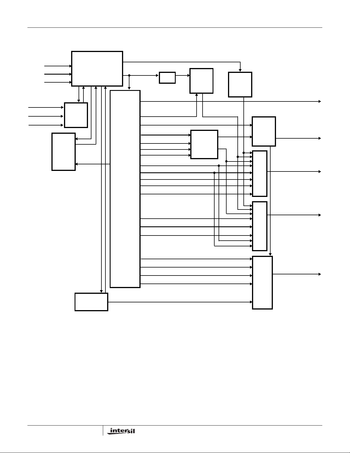
NEW DATA, FIR #
RESET
SYNC
THRESHOLD
DECREMENT 1
DECREMENT 2
LOOP
COUNTER
INSTRUCTION RAM,
SEQUENCER
WAIT
COUNTER
LOOP
COUNTER
PRELOAD
FIR# - WRITE DESTINATION
FIR# - COMPUTE
DATA ADDRESS STEP SIZE
COMPUTE TO COMPUTE
FIR TYPE
NUMBER OF OUTPUTS
TAPS/OUTPUT
READS/TAP
INSTR/TAP
RAM ADDR BLOCK START
RAM ADDR BLOCK SIZE
RAM ADDR STEP SIZE 1
FIR
PARAMETER
RAM
RAM ADDR STEP SIZE 2
RAM ADDR BLOCK TO BLOCK STEP
RAM ADDR INITIAL OFFSET
RAM ADDR OFFSET STEP
RAM ADDR BLOCK TO BLOCK STEP
ALIAS
MASK
READ
POINTER
REG
FILE
START ADDRESS
COMPUTE
COUNTERS
WRITE
POINTER
REG
FILE
FIR OUTPUT DESTINATION
DATA
PATH
CONTROL
ROM
RAM
ADDR
GEN
A
RAM
ADDR
GEN
B
CONTROL SIGNALS
DATA RAM A
READ/WRITE
DATA RAM B
READ ADDRESS
ENABLE
OFFSET
DATA PATH
ADDRESS
RESAMPLER
NCO
COEF ADDR BLOCK START
COEF ADDR BLOCK SIZE
COEF ADDR STEP SIZE PER TAP
ADDR STEP SIZE PER OUTPUT
ADDRESS OFFSET
COEF
ADDR
GEN
COEFFICIENT
READ ADDRESS
18
FN6013.3
July 13, 2007

ISL5216
www.BDTIC.com/Intersil
Instruction Bit Fields
INSTRUCTION BIT FIELDS
BIT
POSITIONS FUNCTION DESCRIPTION
8:0 Instruction Instruction Field Bit Mapping
Bit876543210
Type
WAIT00XXXXCCC
FIR 0 1 Start IncrRS DecrSel DecrEn LdLp DecrLp EnU/C
JUMP1JJJJJCCC
(NOPs and loading the loop counter are special cases of the FIR instruction).
XXXX = ignored.
JJJJJ = jump destination (sequence step number).
CCC = condition code.
000 = ! (waitcount ≥ threshold) -- See IWA = *00Ch, bits 9:0 for threshold details.
001 = waitcount ≥ threshold -- See IWA = *00Ch, bits 9:0 for threshold details.
010 = loop counter ≠ 0.
011 = loop counter = 0.
100 = ! (RSCO) (RSCO - resampler NCO carry output).
101 = RSCO.
110 = sync (if enabled) or μP controlled bit.
111 = always.
Start = load parameters and start filter computation, set to zero for no-ops, loop counter loads.
IncrRS = increment resampler during this filter.
DecrSel = selects between two decrement values for the wait counter.
DecrEn = decrement wait count on starting this instruction.
LdLp = load loop counter with the data in the I(20:9) bit field.
DecrLp = decrement loop counter on starting this instruction.
EnU/C = enable U/C counter with this FIR.
14:9 FIR Type FIR Parameter Bit Fields
14:9 FIR type.
000000 NOP.
000001 Decimating FIR, Even Symmetric, Even # Taps.
000010 Decimating FIR, Even Symmetric, Odd # Taps.
000011 Decimating FIR, Odd Symmetric, Even # Taps.
000100 Decimating FIR, Odd Symmetric, Odd # Taps.
000101 Decimating FIR, Asymmetric.
001000 Resampling FIR, Asymmetric.
001001 Interpolating HBF.
100000 Decimating FIR, Complex (Asymmetric).
NOTES:
14. Regular interpolation FIRs are successive runs of a FIR with no data address increment, but with
coefficient start address increments.
15. Decimating HBFs are even symmetric, odd number of taps but with different data step sizes.
16. U/C FIR is a normal FIR with the U/C bit enabled.
17. Other codes may be added in the future.
17:15 Steps per FIR Specifies the number of steps per FIR instruction sequence (load with value minus 1)
(set to 0 for all FIR types except complex which is set to 1).
Increments on start or at each FIR output depending on μPcontrol bit.
The start bit should not be set when this bit is set.
This multiplies the data by 1, j, -1, -j.
The multiplication factor changes each time the filter runs.
19
FN6013.3
July 13, 2007

ISL5216
www.BDTIC.com/Intersil
INSTRUCTION BIT FIELDS (Continued)
BIT
POSITIONS FUNCTION DESCRIPTION
28:18 Destination Destination Field Bit Mapping
31:29 Round Select 31:29 Round Select (Add rounding bit at specified location).
41:32 Data Memory
Block Start
44:42 Data Memory
Block Size
52:45 Data Memory
Block-to-Block Step
62:53 Coefficient Memory
Block Start
28 27 26 25 24 23 22 21 20 19 18
AGCLFGN AGCLF Path1 Path0 OS FB F4 F3 F2 F1 F0
AGCLFGN AGC loop gain select. Only applies to Path 1.
AGCLF AGC loop filter enable. Only applies to Path 1. The AGC loop is updated with the magnitude
Path(1:0) Back End Data Routing Path Selection. (see Back End Data Routing figure)
OS Enable output strobe. Setting this bit generates a data ready signal when the data reaches
FB Feedback data path. When set, the magnitude and dphi/dt from the cartesian-to-polar coor-
F(4:0) Filter select. For data recirculated to the input of the FIR processor by path 0 or from the
000 2
001 2
010 2
011 2
100 2
101 2
110 2
111 no rounding.
Provided for use with the coefficient down-shift bits.
Memory block base address, 0-1023, 0-383 are valid for the ISL5216.
44:42 Block Size.
0 8
1 16
2 32
364
4 128
5 256
6 512
7 1024
(modulo addressing is used).
0-255, usually equal to the decimation factor for the FIR in this instruction.
Memory base address of coefficients, 0-1023, 0-511 are valid on the ISL5216.
Loop gain 0 or 1 if AGCLF bit is set. Set to 0 (1 is a test mode for future chips).
of this sample (Path(1:0) = 01).
00 Route output back to filter compute engine input to another FIR in the filter chain.
01 Route output thru the FIFO and AGC to outputs I1 and Q1.
10 Route output to I2 and Q2, bypassing the FIFO and AGC. This path
also routes to next channel FIR input.
11 Route output thru the FIFO and AGC to outputs I2 and Q2.
the output section and starts the serial output sequence (paths 1, 2, 3). If OS is not set,
there will be no output to the outside world from this channel, for that output calculation, but
the data will be loaded into its output holding register (OS would not be set when routing the
data to another back end when cascading channels).
dinate converter block are routed to the filter compute engine input (magnitude goes to the
I input and dphi/dt goes to the Q input). Provided for discriminator filtering.
cartesian to polar coordinate converter output, these bits tell which filter sequencer step
gets it as an input.
-24
, use this code when downshifting is not used.
-23
-22
-21
-20
-19
-18
20
FN6013.3
July 13, 2007

ISL5216
www.BDTIC.com/Intersil
INSTRUCTION BIT FIELDS (Continued)
BIT
POSITIONS FUNCTION DESCRIPTION
63 Reserved Set to 0.
66:64 Coefficient Memory
Block Size
75:67 Number of FIR
Outputs
84:76 Read Address
Pointer Step
93:85 Initial Address Offset Initial address offset (to ADDRB). This is the offset from the start address to other end of filter.
95:94 Reserved Set to 0
104:96 Memory Reads Per
FIR Output
106:105 Clocks Per
Memory Read
115:107 Data Memory
Step Size 1
117:116 Data Memory
Step Size 2
119:118 Data Memory
Address Offset Step
122:120 Coefficient Memory
Step Size
66:64 Memory Block Size
08
116
2 32
364
4 128
5 256
6 512
7 1024
(Modulo addressing can be used, but is usually not needed. If not needed this bit field can always be
set to 7).
Number of FIR outputs (range is 1 to 512, load w/ desired value minus 1).
This is usually equal to the total decimation that follows the filter.
Read address pointer step (for next run). This is usually equal to the filter decimation times the number
of outputs from the instruction.
For symmetric filters, usually equal to -1 x (number of taps -1).
This is based on the number of taps (load with value below minus 1).
Value
Type
Symmetric, even number of taps (taps/2) or floor((taps+1)/2).
Symmetric, odd number of taps (taps+1)/2 or floor((taps+1)/2).
Decimating HBF (taps+5)/4.
Asymmetric taps.
Complex taps .
Resampling taps/phase (six taps per phase for the ROM’d coef ficient s provided).
Interpolating HBF (taps+5)/4-1 .
Set to 0 for all but complex FIR, which is set to 1.
(ADDRA) Step size for all but the last tap computation of the FIR.
Set to -2 for HBF, -1 otherwise.
(ADDRA) Step size for last tap computation. Set to -1.
117:116 Step size
0 0
1 -1
2 -2
3 step size value.
(ADDRB) Step size for opposite end of symmetric filter. Set to +2 for Decimating HBF, to +1 for others
(the B data is not used for asymmetric, resampling, and complex filters).
(ADDRC) Usually set to 1.
122:120 Step size
00
1 1
2 2
34
4 8
5 16
6 32
764
21
FN6013.3
July 13, 2007

ISL5216
www.BDTIC.com/Intersil
INSTRUCTION BIT FIELDS (Continued)
BIT
POSITIONS FUNCTION DESCRIPTION
125:123 Coefficient Memory
Block-to-Block Step
127:126 Reserved Set to 0
(ADDRC) Usually set to 0.
125:123 Step size
0 0
1 1
2 2
3 4
4 8
5 16
6 32
7 64
Basic Instruction Set Examples
1. Wait for number of input samples > threshold
127:9 = 0
8:0 = 001
0000,0000,0000,0001h
2. Jump unconditional
127:9 = 0
8:0 = 1JJJJJ111b
example: jump to step 0= 0000,0000,0000,0107h
3. Jump RSCO (jump on resampler NCO carry output)
127:9 = 0
8:0 = 1JJJJJ101b
example: jump RSCO, step 0= 0000,0000,0000,0105h
4. Jump RSCO
127:9 = 0
(jump on no resampler NCO carry output)
0 - WAIT FOR ENOUGH SAMPLES
0000 0000 0000 0000 0000 0000 0000 0000 127:96 00000000h
0000 0000 0000 0000 0000 0000 0000 0000 95:64 00000000h
0000 0000 0000 0000 0000 0000 0000 0000 64:32 00000000h
0000 0000 0000 0000 0000 0000 0000 0001 31:0 00000001h
1 - FIR
0000 0001 0101 1111 1111 100R RRRR RRRR 127:96 015FF---h
00TT TTTT TTTD DDDD DDDD 0000 0000 0111 95:64 -----007h
0000 1000 0000 0000 0000 1010 0000 0000 63:32 08000A00h
0000 1011 0000 0000 0FFF FFF0 1100 1000 31:0 0B00--C8h
2 - JUMP TO STEP 0
0000 0000 0000 0000 0000 0000 0000 0000 127:96 00000000h
0000 0000 0000 0000 0000 0000 0000 0000 95:64 00000000h
0000 0000 0000 0000 0000 0000 0000 0000 64:32 00000000h
0000 0000 0000 0000 0000 0001 0000 0111 31:0 00000107h
Four bit fields must be filled in:
F - filter type (this example applies to types 1-5)
D - decimation (also loaded into wait threshold)
T - number of taps minus 1
R - clocks/calculation (=floor((taps+1)/2) for symmetric, = taps for asymmetric)
The rest of the instruction RAM would typically be filled with NOP instructions:
0000 0000 0000 0000 0000 0000 0000 0000 127:96 00000000h
0000 0000 0000 0000 0000 0000 0000 0000 95:64 00000000h
0000 0000 0000 0000 0000 0000 0000 0000 64:32 00000000h
0000 0000 0000 0000 0000 0000 1000 0000 31:0 00000080h
8:0 = 1JJJJJ100b
example: jump RSCO
, step 0 = 0000,0000,0000,0104h
5. NOP single clock
127:9 = 0
8:0 = 010000000b
NOP1 = 0000,0000,0000,0080h
6. Load Loop Counter
127:21 = 0
20:9 = Loop counter preload (tested against 0)
8:0 = 010000100b
example: LdLpCntr 14 = 0000,0000,0000,1C84h
Single FIR Basic Program
This is the basic program for a single FIR. This program
applies to decimation filters (including DECx1) that are
symmetric or asymmetric (but not complex). The FIR output
is routed through path A with the AGC enabled.
22
FN6013.3
July 13, 2007

Wait Preload Register
www.BDTIC.com/Intersil
This register (IWA register *00Ch) holds the wait counter
threshold and two wait counter decrement values. Each is
ten bits. The wait counter counts filter input samples until the
count is greater than or equal to the threshold. The wait
counter then asserts a flag to the filter compute engine.
The wait counter threshold is typically set to the total number
of input samples needed to generate a filter output. A “WAIT”
instruction in the filter compute engine waits for the wait
counter flag signal before proceeding. The filter compute
engine would then compute all the filters needed to produce
an output and then would jump back to the “WAIT”
instruction.
The wait counter is implemented with an accumulator. This
allows the count to go beyond the threshold without losing
the sample count. Two bits in the FIR instruction decrement
the wait counter (subtract a value) and select the decrement
value. The decrement value is typically the number of
samples needed for an output (total decimation), though it
can be a different value to ignore inputs and shift the timing.
(The read pointer increment must be adjusted as well.)
The filter compute engine sequencer does not count each
input sample or track whether each filter is ready to run.
Instead, the wait counter is used to determine whether there
are enough input samples to compute all the filters in the
chain and get an output sample from the entire filter chain.
This adds some additional delay since intermediate results
are not precalculated, but it simplifies the filter control. The
number of samples needed is equal to the total decimation
of the filter chain. For example, with two decimate-by-2
halfband filters and a decimate-by-2 shaping FIR, the total
decimation would be 8 so 8 samples are needed to compute
an output. HBF1 would compute four times to generate four
inputs to HBF2. HBF2 would compute twice to generate the
two samples that the shaping FIR needs to compute an
output.
Resampler
The resampler is an NCO controlled polyphase filter that allows
the output sample rate to have a non-integer relationship to the
input sample rate. The filter engine can be viewed conceptually
as a fixed interpolate-by-32 filter, followed by an NCO controlled
decimator. The Resampler NCO is similar to the carrier NCO
phase accumulator but does not include the SIN/COS section.
It provides the resampler output pulse and associated phase
information to logic that determines the nearest of the 32
available phase points for a given output sample.
The center frequency (output sample rate) control is double
buffered, i.e., the control word is written to one register via the
microprocessor interface and then transferred to another
(active) register on a write to the timing NCO center frequency
update strobe location (IWA register *009h) or on a SYNC I (if
enabled). As it is not possible to represent some frequencies
ISL5216
exactly with an NCO and therefore, phase error accumulates
eventually causing a bit slip, the phase accumulator length
has been sized to where the error is insignificant. At a
resampler input rate of 1MHz, half an LSB of error in loading
the 56-bit accumulator is 7*10
accumulated phase error is only 0.2*10
degree). The NCO update by the filter compute engine is
typically at the resampler's input rate, and is enabled by the
IncrRS bit in the filter instruction word. The NCO then rolls
over at a fraction of the resampler input rate. The output
sample rate is (f
rate and N is the phase accumulated per resampler input
sample (IWA registers *007h and *008h). N must be between
40000000000000h and FFFFFFFFFFFFFFh corresponding
to decimations from 4 to (1 + 2
however, a range of 80000000000000 h to
FFFFFFFFFFFFFFh (providing decimation from 2 to (1 + 2
respectively) is sufficient for most applications since integer
decimation can be done more efficiently in the preceding CIC
and halfband filters. The resampler changes the sample rate
by computing an output at each input which causes the NCO
to roll over. If an output is to be computed, the nea rest of the
32 available points from the polyphase structure is used.
Because outputs are generated only on input samples which
cause an NCO roll over, output samples will i n genera l not be
evenly spaced. The FIFO/TIMER block between the filter
compute engine and the AGC is provided to improve output
sample spacing for presentation to the serial data output
formatter section (see IWA=*00Ah bit s 11:0 description). If
D/A converted directly, there would be artifacts from the
uneven sample spacing, but if the samples are stored and
reconstructed at the proper rate (the NCO rollover rate), the
signal would have only the distortion produced by
interpolation image leakage and the time quantization (phase
jitter) due to the finite number of interpolation filter phases.
The polyphase filter has 192 coefficients implemented as 32
phases, each of which having 6 taps (6 x 32 = 192). These
coefficients are provided in Table 54. The stopband
attenuation of the filter is greater than 60dB, as shown in
Figures 18 through 20. The signal to total image power ratio
is approximately 55dB, due to the aliasing of the
interpolation images. If the output is at least 2x the baud
rate, the 32 interpolation phases yield an effective sample
rate of 64x the baud rate or approximately 1.5% (1/64
resampler input sample period) maximum timing error.
/ 256)*N, where f
IN
-12
degrees. After one year , the
-3
of a bit (<1/10 of a
is the resampler input
IN
-56
), respectively. Generally,
-56
AGC
The AGC Section provides gain to small signals, after the
large signals and out-of-band noise have been filtered out, to
ensure that small signals have sufficient bit resolution in the
output formatter. The AGC can also be used to manually set
the gain. The AGC optimizes the bit resolution for a variety of
input amplitude signal levels. The AGC loop automatically
adds gain to bring small signals from the lower bits of the
),
23
FN6013.3
July 13, 2007

ISL5216
www.BDTIC.com/Intersil
24-bit programmable FIR filter output into the range of 20-bit
and shorter words in the output section. Without gain control,
a signal at -72dBFS = 20log
10
-12
(2
) at the input would have
only 4 bits of resolution at the output if a 16 bit word length
were to be used (12 bits less than the full scale 16 bits). The
potential increase in the bit resolution due to processing gain
of the filters can be lost without the use of the AGC.
Figure 4 shows the Block Diagram for the AGC Section. The
FIR filter data output is routed to the Cartesian to polar
coordinate converter after passing through the AGC
multipliers and shift registers. The magnitude output of the
Cartesian to polar coordinate converter is routed through the
AGC error detector, the AGC error scaler and into the AGC
loop filter. This filtered error term is used to drive the AGC
multiplier and shifters, completing the AGC control loop.
The AGC multiplier/shifter portion of the AGC is identified in
Figure 4. The gain control from the AGC loop filter is
SERIAL
OUT
μP
(11 MANTISSA
4 EXPONENT)
AGC LOOP FILTER
19
MSB = 0
16
REGISTER
MSB = 0
4
EXP=2
EN
18
NNNN
M
U
X
REGISTER
AGC
LOAD
MANTISSA =
16
01.XXXXXXXXXXXXXX
μP
(RANGE = -2.18344 TO 2.18344)
LIMITER
LIMIT
DET
UPPER LIMIT
LOWER LIMIT †
LIMIT
DET
sampled when new data enters the multiplier/shifter. The
limit detector detects overflow in the shifter or the multiplier
and saturates the output of I and Q data paths
independently. The shifter has a gain from 0 to 90.31dB in
6.021dB steps, where 90.31dB = 20log
(2N ) when
10
N = 15. The mantissa provides up to an additional 6.02dB of
gain. The gain in dB from the mantissa is:
20log
[1 + (X)2
10
-14
], where X is the fractional part of the
mantissa interpreted as an unsigned integer ranging from 0
14
to 2
- 1.
Thus, the AGC multiplier/shifter transfer function is
expressed as:
AGC Mult/Shift Gain = 2
N
[1 + (X)2
-14
]
where N, the shifter exponent, has a range of 0 < N < 15 and
X, the mantissa, has a range of 0 < X < (2
AGC ERROR SCALING
+
28
AGCGNSEL
EXP
SHIFT
4
MANTISSA
4
14
-1).
AGC
ERROR
DETECTOR
16
Δ
†
EXP †
†
LOOP GAIN 0
MAN
(RANGE = 0 TO 1)
† EXP †
LOOP GAIN 1
AGC REGISTER 0
(RANGE = 0 TO 2.32887)
MAN
AGC REGISTER 1
MAGNITUDE
(S = 0)
UNSIGNED †
THRESHOLD
STT.TTTTTTTTTTTTT
16
IFIR
QFIR
24
24
24
SHIFTER
24
SHIFTER
AGC MULTIPLIER/SHIFTER
LIMITER
IAGC
LIMIT
DET
LIMITER
24
24
QAGC
† Controlled via microprocessor interface.
FIGURE 4. AGC FUNCTIONAL BLOCK DIAGRAM
24
CARTESIAN
TO
POLAR
COORDINATE
CONVERTER
(G = 1.64676)
FN6013.3
July 13, 2007

ISL5216
www.BDTIC.com/Intersil
In dB, this can be expressed as:
(AGC Mult/Shift Gain)dB = 20 log10(2N[1 + (X)2
The full AGC range of the multiplier/shifter is from 0dB to
20log
The 16 bit resolution of the mantissa provides a theoretical
AM modulation level of -96dBc (depending on loop gain,
settling mode and SNR). This effectively eliminates AM
spurious components caused by the AGC resolution.
The Cartesian to polar coordinate converter accepts I and Q
data and generates magnitude and phase data. The
magnitude output is determined by the equation:
where the magnitude limits are determined by the maximum
I and Q signal levels into the Cartesian to polar converter.
Taking fractional 2's complement representation, magnitude
ranges from 0 to 2.329, where the maximum output is
The AGC loop feedback path consists of an error detector,
error scaling, and an AGC loop filter. The error detector
subtracts the magnitude output of the coordinate converter
from the programmable AGC THRESHOL D value. Th e AGC
THRESHOLD value is set in IWA register *012h and is equal
to 1.64676 times the desired magnitude of the I1/Q1 output.
Note that the MSB is always zero. The range of the AGC
THRESHOLD value is 0 to +3.9999. The AGC Error
Detector output has the identical range.
The loop gain register values adjust the response/settling
time of the AGC loop. The loop gain is set in the AGC Error
Scaling circuitry, using four values in two sets of
programmable mantissa and exponent pairs (see IWA
register *010h). Each set has both an attack and a decay
gain. This allows asymmetric adjustment for applications
such as VOX systems where the signal turns on and off. In
these applications, the gains would be set for fast attack and
slow decay so that the part decreases the gain quickly when
the signal turns on, but increases the gain slowly when the
signal turns off (in anticipation of it turning back on shortly).
For fixed gains, either set the upper and lower AGC limits to
the same value, or set the limits to minimum and maximum
gains and set the AGC attack and decay loop gains to zero.
The mantissa, M, is a 4-bit value which weights the loop filter
input from 0.0 to 15/2
shift factor that provides additional weighting from 2
Together the mantissa and exponent define the loop gain as
given by,
AGC Loop Gain = M
where M
to 15, and E
0 to 15. The composite (shifter and multiplier) AGC scaling
[1 + (214 -1)2
10
r 1.64676 I2Q2+=
r 1.64676 1212+ 1.64676x1.414 2.329===
is a 4-bit binary mantissa value ranging from 0
LG
LG
-14
] + 20log 10 [215 ] = 96.329dB.
4
= 0.9375. The exponent, E, defines a
-(15-ELG)
2-4 2
LG
is a 4-bit binary exponent value ranging from
-14
])
0
to 2
-15
Gain range is from 0.0000 to 2.329(0.9375)20 = 0.0000 to
2.18344. The scaled gain error can range (depending on
threshold) from 0 to 2.18344, which maps to a “gain change
per sample” range of 0 to 3.275dB/sample.
The AGC attack and decay gain mantissa and exponent values
for loop gains 0 and 1 are programmed into IWA register *010h.
The PDC provides for the storing of two values of AGC attack
and decay scaling gains to allow for quick adjustment of the
loop gain by simply setting IWA register *013h bits 9 and 10
accordingly. Possible applications include acquisition/tracking,
no burst present/burst present, strong signal/weak signal,
track/hold, or fast/slow AGC values.
The AGC loop filter consists of an accumulator with a built in
limiting function. The maximum and minimum AGC gain
limits are provided to keep the gain within a specified range
and are programmed by 16-bit upper and lower limits using
the following the equation:
-12
AGC Gain Limit = (1 + m
(AGC Gain Limit)dB = (6.02)(eeee) + 20 log(1.0+0.mmmm
mmmm mmmm)
where m is a 12-bit mantissa value between 0 and 4095, and
e is the 4-bit exponent ranging from 0 to 15. IWA register
*011h Bits 31:16 are used for programming the upper limit,
while bits 15:0 are used to program the lower limit. The
format for these limit values are:
(31:16) or (15:0): E E E E M M M M M M M M M M M M
for a gain of 0 1. M M M M M M M M M M M M * 2
and the possible range of AGC limits from the previous
equations is 0 to 96.328dB. The bit weightings for the AGC
Loop Feedback elements are detailed in Table 55.
Using AGC loop gain, the AGC range, and expected error
detector output, the gain adjustments per output sample for
the loop filter section of the digital AGC can be given by
AGC Slew Rate = (1.5 dB) (THRESHOLD - (MAG *
1.64676)) x (M
The loop gain determines the growth rate of the sum in the
loop accumulator which, in turn, determines how quickly the
AGC gain scales the output to the threshold value. Since the
log of the gain response is roughly linear, the loop response
can be approximated by multiplying the maximum AGC gain
error by the loop gain. The expected range for the AGC rate
is ~ 0.000106 to 3.275dB/output sample time for a threshold
of 1/2 scale. For a full scale error, the minimum non-zero
.
AGC slew rate would be approximately 0.0002dB/output or
20dB/sec at 100ksps. The maximum gain would be
6dB/output. This much gain, however, would probably result
in significant AM on the output.
The maximum AGC Response is given by:
AGC Response
Gain)(AGC Loop Gain)(AGC Output Weighting)
LG
Max
AGC
) (2-4) (2
-(15 - ELG)
= (Input)(Cart/Polar Gain)(Error Det.
e
2
) 2
E E E E
)
25
FN6013.3
July 13, 2007

ISL5216
www.BDTIC.com/Intersil
The loop gain mantissas and exponents are set in IWA
register *010h, with IWA register *013h selecting loop gain 0
or 1 and the settling mode.
In the ISL5216, a SYNCI signal will clear the AGC loop filter
accumulator if GWA register F802h bit 27 is set. This sets
the AGC to unity gain or to the lower gain limit (IWA *011h
bits 15:0) if it is larger than unity.
The settling mode of the AGC forces either the mean or the
median of the signal magnitude error to zero, as selected by
IWA register *013h bit 8. For mean mode, the gain error is
scaled and used to adjust the gain up or down. This
proportional scaling mode causes the AGC to settle to the
final gain value asymptotically. This AGC settling mode is
preferred in many applications because the loop gain
adjustments get smaller and smaller as the loop settles,
reducing any AM distortion caused by the AGC.
With this AGC settling mode, the proportional gain error
causes the loop to settle more slowly if the threshold is
small. This is because the maximum value of the threshold
minus the magnitude is smaller. Also, the settling can be
asymmetric, where the loop may settle faster for “over
range” signals than for “under range” signals (or vice versa).
In some applications, such as burst signals or TDMA signals,
a very fast settling time and/or a more predictable settling
time is desired. The AGC may be turned off or slowed down
after an initial AGC settling period.
The median mode minimizes the settling time. This mode
uses a fixed gain adjustment with only the direction of the
adjustment controlled by the gain error. This makes the
settling time independent of the signal level.
For example, if the loop is set to adjust 0.5dB per output
sample, the loop gain can slew up or down by 16dB in 16
symbol times, assuming a 2-samples-per-symbol output
sample rate. This is called a median settling mode because
the loop settles to where there is an equal number of
magnitude samples above and below the threshold. The
disadvantage of this mode is that the loop will have a wander
(dither) equal to the programmed step size. For this reason,
it is advisable to set one loop gain for fast settling at the
beginning of the burst and the second loop gain for small
adjustments during tracking.
In the median mode, the maximum gain step is
approximately 3dB/output. The step is fixed (it does not
decrease as the error decreases) so a large gain will cause
AM on the output at least that large. The fixed gain step is
set by the programmable AGC loop gain register
IWA *010h.
The AGC gain limits register sets the minimum and
maximum limits on the AGC gain. The total AGC gain range
is 96dB, but only a portion of the range should be needed for
most applications. For example, with a 16-bit output to a
processor, the 16 bits may be sufficient for all but 24dB of
the total input range possible. The AGC would only need to
have a range of 24dB. This allows faster settling and the
AGC would be at its maximum gain limit except when a high
power signal was received. The AGC may be disabled by
setting both limits to the same value.
The median settling mode is enabled by setting IWA register
*013h bit 8 to 0 while the mean loop settling mode is
selected by setting bit 8 to 1.
Cartesian to Polar Converter
The Cartesian to Polar converter computes the magnitude
and phase of the I/Q vector. The I and Q inputs are 24 bits
wide. The converter phase output is 18 bits wide and is
routed to the output formatter and frequency discriminator.
This 18-bit output phase can be interpreted either as two’s
complement (-0.5 to approximately 0.5) or unsigned (0.0 to
approximately 1.0), as shown in Figure 5. The phase
conversion gain is 1/2π. The 24-bit magnitude is unsigned
binary format with a range from 0 to 2.32. The magnitude
conversion gain is 1.64676. The MSB of the magnitude (the
sign bit) is always zero.
+π/2
400000
7fffff
±π
800000
FIGURE 5. PHASE BIT MAPPING OF COORDINATE
3fffff
Q
000000
I
0
ffffff
c00000
bfffff
-π/2
CONVERTER OUTPUT
7fffff
π
800000
400000
bfffff
π/2
c00000
3π/2
3fffff
Q
I
000000
0
ffffff
26
FN6013.3
July 13, 2007

ISL5216
www.BDTIC.com/Intersil
T able 1 details the phase and magnitude weighting for the 16
bits output from the PDC.
TABLE 1. MAG/PHASE BIT WEIGHTING
o
BIT MAGNITUDE PHASE (
23 (MSB) 2
22 2
21 2
20 2
19 2
18 2
17 2
16 2
15 2
14 2
13 2
12 2
11 2
10 2
92
82
72
62
52
42
32
22
12
0 (LSB) 2
2
1
0
-1
-2
-3
-4
-5
-6
-7
-8
-9
-10
-11
-12
-13
-14
-15
-16
-17
-18
-19
-20
-21
180
90
45
22.5
11.25
5.625
2.8125
1.40625
0.703125
0.3515625
0.17578125
0.087890625
0.043945312
0.021972656
0.010986328
0.005483164
0.002741582
0.001370791
0.0006853955
0.00034269775
0.00017134887
0.00008567444
0.00004283722
0.00002141861
)
The magnitude and phase computation requires 17 clocks
for full precision. At the end of the 17 clocks, the magnitude
and phase are latched into a register to be held for the next
stage, either the output formatter or frequency discriminator.
If a new input sample arrives before the end of the 17 cycles,
the results of the computations up until that time, are
latched. This latching means that an increase in speed
causes only a decrease in accuracy. Table 2 details the
exact accuracy that can be obtained with a fixed number of
clock cycles up to the maximum of 17. The input magnitude
and phase errors induced by normal SNR values will almost
always be worse than the Cartesian to Polar conversion.
TABLE 2. MAG/PHASE ACCURACY vs CLOCK CYCLES
MAGNITUDE
ERROR
CLOCKS
60.0653.5 2
70.0161.8 1
8 0.004 0.9 0.5
9 <0.004 0.45 0.25
10 <0.004 0.22 0.12
11 <0.004 0.11 0.062
12 <0.004 0.056 0.03
13 <0.004 0.028 0.016
14 <0.004 0.014 0.008
15 <0.004 0.007 0.004
16 <0.004 0.0035 0.002
17 <0.004 0.00175 0.001
† Assumes ±180° = f
(% f
.
S
)
S
PHASE
ERROR
†
(°)
PHASE
ERROR
(% f
S
)
27
FN6013.3
July 13, 2007

Serial Data Output Formatter Section
www.BDTIC.com/Intersil
OUTPUT SECTION
ZERO
I1
Q1
MAG
PHASE
Q2
GAIN
STROBE
R
E
I2
G
ZERO
M
U
X
DELAY
M
U
X
ISL5216
FIXED
TO
FLOAT
ROUND
M
U
X
SEQUENCER
1
ROUND
SEQUENCER
2
PARALLEL
TO
SERIAL
PARALLEL
TO
SERIAL
TO/FROM
OTHER CHANNELS
SYNC
GEN
&
&
O
R
&
&
&
&
O
R
&
&
&
&
O
R
&
&
SD1x
SYNCx
SD2x
16
M
U
X
NOTE: Each serial output has 7 time slots. Each slot can contain I1, Q1, I2, Q2, Mag, phase or dφ/dt, AGC gain, or zeros. Each slot can be 4, 6, 8,
10, 12, 16, 20, 24, or 32 (24 + 8 zeros) bits or disabled. Output 1 can also be 32-bit floating point. Slots can be disabled. A disabled slot will be one
clock wide if there are other active slots following. A sync can be asserted with any or all slots in output 1. The serial output can be delayed from 0
to 4095 serial clock periods from the input strobe. The serial outputs are always MSB first. The sync position applies to all time slots and can be one
clock prior to the first data bit, aligned with the first data bit, or one clock after the last data bit.
Serial Data Output Control Register
The serial data output control register contains sync position
and polarity (SYNCA, B, C or D), channel multiplexing, and
scaling controls for the SD1x and SD2x (x = A, B, C or D)
serial outputs (see Microprocessor Interface section, IWA
register *014h).
TO μP
INTERFACE
each of the SD2 serial output sections (the syncs are only
associated with the SD1 serial outputs). There, the four
outputs are AND-ed with the multiplexing mask programmed
in the serial data output control registers of channels 0 thru 3
and OR-ed together. By gating off the channels that are not
wanted and delaying the data from each desired channel
appropriately, the channels can be multiplexed into a
Channel Routing Mask
The multiplexing mask bits for each channel (see
Microprocessor Interface section, IWA register *014h bits
19:16 for SD1x or bits 15:12 for SD2x) can be used to
enable that channel’s output to any of the four serial outputs.
These bits control the AND gates that mask off the channels,
so a zero disables the channel’s connection to that output.
common serial output stream. It should be noted that in
order to multiplex multiple channels onto a single serial data
stream the channels to be multiplexed must be synchronous.
Serial Data Output Time Slot Content/Format
Registers
These four registers are used to program the content and
format of the serial data output sequence time slots (see
To configure more than one channel's output onto a serial
data output, the SD1 serial outputs and syncs from each
channel (0, 1, 2 and 3) are brought to each of the SD1 serial
Microprocessor Interface section, IWA registers *015h *018h). There are seven data time slots that make up a
serial data output stream. The number of data bits and data
output sections and the SD2 serial outputs are brought to
28
FN6013.3
July 13, 2007

ISL5216
www.BDTIC.com/Intersil
format of each slot is programmable as well as whether
there will be a sync generated with the time slot (the syncs
are only associated with the SD1 serial outputs). Any of
seven types of data or zeros can be chosen for each time
slot. Eight bits are used to specify the content and format of
each slot.
As an example, suppose we wanted to output 32-bit I and Q
values from channels 0 and 1 into the SD1A serial data
output stream, we would program the following settings in
the channel’s serial data output control and content/format
registers:
Channel 0:
delay = 0 (IWA = 0014h, bits 11:0 = 0);
first data time slot = I, 32-bit, sync pulse generated
(IWA = 0015h, bits 7:0 = 0xC9);
second data time slot = Q, 32-bit, no sync pulse
(IWA = 0015h, bits 15:8 = 0x4A);
third through seventh data time slot = zero and no sync,
(IWA = 0015h, bits 31:16 = 0 and IWA = 0016h, bits
31:0 = 0);
enable the SD1A serial output for this channel in the serial
routing mask (IWA = 0014h, bit 16 = 1).
Channel 1:
delay = 64 (IWA = 1014h, bits 11:0 = 0x40);
first data time slot = I, 32-bit, sync pulse generated
(IWA = 1015h, bits 7:0 = 0xC9);
second data time slot = Q, 32-bit, no sync pulse
(IWA = 1015h, bits 15:8 = 0x4A);
third through seventh data time slot = zero and no sync,
(IWA = 1015h, bits 31:16 = 0 and IWA = 1016h, bits
31:0 = 0);
The resulting order is CH0 I first, then CH0 Q, CH1 I, and
CH1 Q with sync pulses generated in the I data slots. The
position of the sync pulses relative to the data slot may be
programmed with IWA register *014h bits 25:24.
Setting delay = 64 offsets channel 1’s 32-bit I and Q data by
64 clocks so that it immediately follows the 64 bits of data
from channel 0. In this way channel 1’s first and second time
slots follow channel 0’s second time slot.
Instead of using the delay to offset channel 1’s data, channel
0 could have been configured to output 32 bits of I in the first
slot, 32 bits of Q in the second slot, 32 bits of zeros in the
third slot and 32 bits of zeros in the fourth slot. Channel 1
could then be configured to output 32 bits of zeros in the first
and second slots, 32 bits of I in the third slot and 32 bits of Q
in the fourth slot. As the channel outputs are OR’d together,
the zero slots do not interfere with data slots.
The ISL5216 Microprocessor (μP) interface consists of a
16-bit bidirectional data bus, P(15:0), three address pins,
ADD(2:0), a write strobe (WR
chip enable (CE
configuration of the ISL5216. The control and configuration
data to be loaded is first written to a 32-bit holding register at
direct (external) addresses ADD(2:0) = 0 and 1, 16 bits at a
time. The data is then transferred to the target register,
synchronous to the clock, by writing the indirect (internal)
address of the target register to direct (external) address 2,
ADD(2:0) = 2. The interface generates a synchronous one
clock cycle wide strobe to transfer the data contained in the
holding register to the target register. The synchronization
and write process requires four clock periods. New data
should not be written to the holding register until after the
synchronization period is over.
). Indirect addressing is used for control and
), a read strobe (RD) and a
enable the SD1A serial output for this channel in the serial
routing mask (IWA = 1014h, bit 16 = 1).
29
FN6013.3
July 13, 2007

Microprocessor Interface
www.BDTIC.com/Intersil
ISL5216
RD
P(15:0)
WR
A(2:0)
CLK
CE
(GATING NOT SHOWN)
MUX
3 2 1 0
15:0
31:16 31:0 INTERNAL READ DATA BUS
FROM OUTPUT FIFO
STATUS
L
A
T
C
H
D
E
C
O
D
E
= 0
= 1
= 2 or 3
= 2
en
en
en
RST
15:0 31:0
R
E
G
>
31:16
R
E
G
>
R
E
G
>
F
F
>
M
U
X
E
S
INTERNAL
WRITE DATA BUS
INTERNAL
ADDRESS BUS
G
A
SYNC’d
F
F
>
F
F
>
F
F
>
SPECIAL LOW
METASTABILITY
CELL
AND
T
I
N
G
TO TARGET
REGISTERS
INTERNAL
READ SIGNAL
WR
Data reads can be direct, indirect or FIFO-like depending on
the data that is being read. The status register is read
directly at direct (external) address 3, ADD(2:0) = 3.
Readback of internal registers and memories is indirect. The
16-bit indirect (internal) address of the desired read source
is first written to direct (external) address 3, ADD(2:0) = 3, to
select the data. The data can then be read at direct
(external) addresses ADD(2:0) = 0 and 1 (bits 15:0 at
address 0 and 31:16 at address 1). The data types available
via the indirect read are listed in the Tables of Indirect Read
Address (IRA) Registers. (Note that the μPHold bit contained
in the target register at Indirect Write Address (IWA) = *00Ah
must be set to suspend the filter compute engine before the
coefficient RAM and instruction bit fields can be written to or
read from.)
The ISL5216 output data from the four channels is available
through the microprocessor interface as well as from the
serial data outputs. A FIFO-like interface is used to read the
output data through the microprocessor interface. When new
output data is available, it is loaded into a FIFO in a user
programmed order (for details on the programming order
see Global Write Address (GWA) = F820h - F83Fh). It can
then be read, 16 bits at a time, at direct address 2, ADD(2:0)
= 2. At the end of each read, the FIFO counter is advanced
to the next location. This allows a DMA controller to read all
of the data with successive reads to a single direct address.
No writes or other interaction is required. The FIFO counter
is reset and reloaded by each interrupt signal, see GWA
F802h. New data in the FIFO is also indicated in the status
register located at direct address ADD(2:0) = 3 if a polled
mode is preferred. The eight data types available, for each of
the four channels, via this interface are: I(23:8), I(7:0)+8
Zeroes, Q(23:8), Q(7:0)+8 Zeroes, Mag(23:8), Mag(7:0)+8
Zeroes, Phase (15:0), and AGC (15:0). The upper bits of I,
i.e., I(23:8), and Q, i.e., Q(23:8), are not rounded to 16 bits.
This interface can read the data from all the channels that
are synchronized. However, because a common FIFO is
used and the FIFO is reset and reloaded by each interrupt, it
cannot be used for asynchronous channels.
The direct address map for the microprocessor interface is
shown in the Table of Microprocessor Direct Read/Write
Addresses and the procedures for reading and writing to this
interface are provided below. The bit field details for each
indirect read and write address is provided in the Table of
Indirect Read Address (IRA) Registers, Tables of Indirect
Write Address (IWA) Registers and Tables of Global Write
Address (GWA) Registers in the following sections.
30
FN6013.3
July 13, 2007

ISL5216
www.BDTIC.com/Intersil
μP Read/Write Procedures
To Write to the Internal Registers:
1. Load the indirect write holding registers at direct address
ADD(2:0) = 0 and 1 with the data for the internal register
(16 or 32 bits depending on the internal register being
addressed).
2. Write the Indirect Write Address of the internal register
being addressed to direct address ADD(2:0) = 2 (Note: A
write strobe to transfer the contents of the Indirect Write
Holding Register into the Target Register specified by the
Indirect Address will be generated internally).
3. Wait four clock cycles before performing the next write to
the indirect write holding registers.
To Write to the Internal Instruction/Coefficient RAMs:
1. Put the filter compute engine of the desired channel into
the hold mode by setting bit 31 of the Filter Compute
Engine/Resampler Control register located at IWA =
*00AH (Note: The * is equal to 0, 1, 2 or 3 depending on
the channel being addressed). By setting bit 31 all FIR
processing for the channel addressed will be stopped.
2. Load the indirect write holding registers at direct address
ADD(2:0) = 0 and 1 with the data for the internal RAM
location.
3. Write the Indirect Write Address of the internal RAM
location being addressed to direct address ADD(2:0) = 2
(Note: A write strobe to transfer the contents of the
Indirect Write Holding Register into the RAM location
specified by the Indirect Address will be generated
internally).
4. Wait four clock cycles before performing the next write to
the indirect write holding registers.
5. After all data has been loaded, set the μPHold bit back
low.
To Read Internal Registers:
1. Write the Indirect Read Address of the internal register
being addressed to direct address ADD(2:0) = 3.
2. Perform a read of the Indirect Read Holding Registers at
direct address ADD(2:0) = 0 and 1.
To Read Data Outputs:
1. Set up the μP FIFO Read Order Control Register (located
at Global Write Address (GWA) = F820H - F83FH).
2. Wait for interrupt or check flag.
3. Data can then be read, 16 bits at a time, at direct
address 2, ADD(2:0) = 2.
4. Repeat step 3 for desired number of words.
5. Go to step 2.
To Read Instruction/Coefficient Values:
1. Put the filter compute engine of the desired channel into
the hold mode by setting bit 31 of the Filter Compute
Engine/Resampler Control register located at
IWA = *00AH (Note: The * is equal to 0, 1, 2 or 3
depending on the channel being addressed).
2. Write the Indirect Read Address (IRA) of the internal
RAM/ROM location being addressed to direct address
ADD(2:0) = 3.
3. Wait four clock cycles.
4. Read the data at direct address ADD(2:0) = 0 and 1.
5. After all the data has been read, set the μPHold bit back
low.
Recommended ISL5216 configuration
procedure following a hardware reset (i.e.
RESETb is pulsed low):
1. Load Global Write Address registers GWA F800H - GWA
F808H and GWA F820H - GWA F83FH.
2. For each signal processing channel (0-3):
a. Set μPHold bit located at Indirect Write Address
register IWA *00AH bit 31.
b. Load Filter Compute Engine Instruction RAMS.
c. Load Filter Compute Engine Coefficient RAMS.
d. Load IWA registers *000H - *019H and *01CH. (Clear
the μPHold bit in register IWA *00AH bit 31).
e. Wait 32 clocks (CLK) for the reset to complete in the
Filter Compute Engine.
3. Generate a SYNCI to enable the input data or to
synchronize the processing to external events or
generate a SYNCO and internal SYNCI by writing to
GWA F80AH. A write to F809H will also work if the
SYNCO pin is externally connected to the SYNCI pin.
Recommended ISL5216 Channel
Reconfiguration Procedure:
1. Disable the serial output for the desired channel in
register GWA F801H - bits 3:0.
2. Disable the interrupts from the channel in register GWA
F802H bits 31, 23, 15, and 7.
3. Set the μPHold bit in register IWA *00AH bit 31 to give the
processor access to the Filter Compute Engine
Instruction RAMS and Coefficient RAMS.
4. Load the new filter configuration.
5. Load any other channel registers.
6. Clear the μPHold bit in register IWA *00AH bit 31.
7. Do a software channel reset by writing to IWA *019H.
8. Enable the serial outputs (GWA F801H) and interrupts
(GWA F802H).
9. Generate a SYNCI to enable the input data or to
synchronize the processing to external events or
generate a SYNCO by writing to GWA F80AH or F809H
(if SYNCO pin is tied to SYNCI pin).
31
FN6013.3
July 13, 2007

ISL5216
www.BDTIC.com/Intersil
JTAG
JTAG: The IEEE1149.1 Joint Test Action Group boundary
scan standard operational codes shown in Table 3 below are
supported. A separate application note is available with
implementation details.
TABLE 3. JTAG OP CODES SUPPORTED
INSTRUCTION OP CODE
EXTEST 0000
IDCODE 0001
SAMPLE/PRELOAD 0010
INTEST 0011
BYPASS 1111
Built in Self Test
Self-test is initiated by resetting the part and loading a given
configuration register set and filter coefficient set. The selftest replaces the user programmed input with a PN
sequence and calculates a 16 bit signature from the output
data. This signature is compared to a user-provided
signature and the result is provided as a bit in the status
register. The BIST procedure is as follows:
1. Configure the part as described in “Recommended
ISL5216 configuration procedure following a hardware
reset” above.
2. (optional) Load the 16 bit comparison signature into GWA
F80BH bits 15:0. This value will be compared to the
device-calculated signature and reported in the status
register. The device-calculated signature may also be
read and the comparison performed in the user ’s
microcontroller.
3. Write 00000000H to F019H to perform a software reset of
all channels.
4. Write 00000001H to GWA F800H to start the first phase
of the self test.
5. Wait until bit 0 of F800H is cleared indicating the first
phase of self test has completed.
6. Write 00000000H to F019H to reset all channels again.
7. Write 00000001H to GWA F800H to start the second
phase of the self test.
8. Wait until bit 0 of F800H is cleared indicating the second
phase of self test has completed.
9. If a comparison signature has been supplied (step 2), bit
12 of the status register (direct read address register 3) is
set to 1 if the signature matches the ISL5216-generated
signature.
10. The ISL5216-generated signature may be read from
GWA F80BH bits 31:16. The user-supplied signature
(step 2) may be also be read back from bits 15:0.
Filter Compute Engine Data RAM Test
The ISL5216 provides read/write access to the data RAM
used by a channel’s filter compute engine. To access the
data RAM for testing, set bit 15 of GWA F800H. Data must
be written to the RAM in Q/I pairs - 24 bit Q first, then 24 bit I.
Q and I samples are written to the RAM using the indirect
addresses shown in the table below (see To Write to the
Internal Registers above for the indirect write procedure).
Reading of the registers may occur in any order. The table
below provides the valid address range in data RAM test
mode. Note that addresses *000H - *6FFH are valid with the
exception of *300H - *3FFH. * = 0, 1, 2, or 3 for channels 0
through 3, respectively. F800H bit 15 must be cleared after
data RAM testing to return to normal operation.
DATA RAM ADDRESS MAP
INDIRECT ADDRESS (Note 18) DAT A
*000H Q sample 0
*001H I sample 0
*002H Q sample 1
*003H I sample 1
::
*2FEH Q sample 767
*2FFH I sample 767
*300H - *3FFH unused
*400H Q sample 768
*401H I sample 768
*402H Q sample 769
*403H I sample 769
::
*6FEH Q sample 1535
*6FFH I sample 1535
*700H - *7FFH unused
NOTE:
18. Denotes 0, 1, 2 or 3 for channels 0 - 3, respectively.
32
FN6013.3
July 13, 2007

ISL5216
www.BDTIC.com/Intersil
TABLE OF MICROPROCESSOR DIRECT READ/WRITE ADDRESSES
ADD(2:0) PINS REGISTER DESCRIPTION
0 WR Indirect Write Holding Register, Bits 15:0.
1 WR Indirect Write Holding Register, Bits 31:16.
2 WR Indirect Write Address Register for Internal Target Register (Generates a write strobe to transfer contents of the
Write Holding Register into the Target Register specified by the Indirect Address, see also Tables of Indirect
Address Registers).
3 WR Indirect Read Address Register (Used to select the Read source of data - uses the same register as Direct
Address 2 but generates a read strobe (for RAMs and AGC) as needed instead of a write strobe).
0 RD Indirect Read, Bits 15:0.
1 RD Indirect Read, Bits 31:16.
2 RD Read Register (FIFO) - Reads FIFO data from output section (This location reads output data in the order
loaded in Global Control Indirect Address Registers F820-F83F. The FIFO is automatically incremented to the
next data location at the end of each read).
3 RD Status Register
P(15:0) BIT DESCRIPTION
15:13 Unused.
12 BIST signature comparison result: 1= success (signatures match)
11:6 Read non-bus input pins (ENIx
11 RESET (Note: This bit is inverted with respect to the RESET input pin).
10 ENIA
9ENIB
8ENIC
7 ENID.
6 SYNCI.
5:2 Mask revision number. ISL5216 devices return 3 or higher (0, 1 and 2 were used for
HSP50216).
1 Level detector integration done. Active high.
0 New FIFO output data available (used for polling mode vs interrupt mode) Active low.
.
.
.
, RESET, SYNCI).
33
FN6013.3
July 13, 2007

ISL5216
www.BDTIC.com/Intersil
Tables of Indirect Write Address (IWA) Registers
NOTE: These Indirect Write Addresses are repeated for each
channel. In the addresses below, the * field is the channel select
nibble. These bits of the Indirect Address select the target channel
TABLE 4. CHANNEL INPUT SELECT/FORMAT REGISTER (IWA = *000h)
P(31:0) FUNCTION
24 Upper Side Band/Lower Side Band select for use in complex input mode.
23 For complex input mode: when set to 1, the I sample is taken when ENIX
set to 0, Q sample is taken two clocks after ENIX
22 Complex input enable. Set to 1 for complex input mode, 0 for real input mode.
21 If set, adjusts the alignment between input data enables and NCO enables to allow unevenly spaced input samples in the gated input
mode. This may be set to 0 to align processing delays with the HSP50216 if necessary.
20:18 Floating point exponent saturation level. Used with floating point modes to set the maximum exponent code level 000 to 111. These
17 Enables the new (ISL5216) floating point modes -- the 11, 12, 13 and 14-bit modes with 42 dB of gain, and 15 and 16-bit modes with
16 Floating point mode select bit 2. Used with IWA *000, bits 8:7 to select the floating point mode/format. See Floating Point Input Mode
15:13 Channel Input Source Selection - Selects as the data input for the channel specified in the Indirect Address either A(15:0), B(15:0),
12 μP Test Register input enable selection:
11 μP input enable. When bit 12 is set, this bit is the input enable for the μP Test Register input. Active low:
10 Parallel Data Input Format:
8:7 Floating point mantissa size select bits 0 and 1. See Floating Point Input Mode Bit Mapping Tables for details.
bits are protection against overflow due to an invalid exponent for the programmed CIC shift code. Set to 111 to disable.
18 dB and 6 dB ranges, respectively. The X-1 input must be used for 14, 15 and 16-bit modes. See Floating Point Input Mode Bit
Mapping Tables for details.
Bit Mapping Tables for details.
C(15:0), D(15:0) or the μP Test Input register as shown below:
15:13
000 A(15:0)
001 B(15:0)
010 C(15:0)
011 D(15:0)
100 μP Test input register. This is provided for testing and to zero the input data bus when a channel is not in use.
1 Bit 11 of this register is used as the input enable.
0 A one clock wide pulse generated on each write to lGWA F808h is used as the input enable.
Select 0 to write test data into the part.
Select 1 to input a constant or to disable the input for minimum power dissipation when an NCO/mixer/CIC section is unused.
0 Enabled
1 Disabled.
0 Two’s complement (-full scale = 1000...0000, zero = 0000...0000, +full scale = 0111...1111).
1 Offset binary (-full scale = 0000...0000, zero = 1000...0000, +full scale = 1111...1111).
9 Fixed/Floating point:
0 Fixed point.
1 Floating point. The 17-bit input bus is divided into 11 to 16 mantissa bits and 1 to 3 exponent bits depending on bits 17,
SOURCE SELECTED
The Global Write Address register for the μP Test input register is F807h.
16, 8 and 7. See Floating Point Input Mode Bit Mapping Tables for details.
is active.
register for the data. Values of 0 through 3 and F are valid. A channel
select nibble value of F is a special case which writes the data to the
same location in each of the four channels simultaneously.
is active and the Q sample is taken on the next clock. When
34
FN6013.3
July 13, 2007

ISL5216
www.BDTIC.com/Intersil
TABLE 4. CHANNEL INPUT SELECT/FORMAT REGISTER (IWA = *000h) (Continued)
P(31:0) FUNCTION
6:4 De-multiplex control. These control bits are provided to select a channel from a group of multiplexed channels. Up to eight multiplexed
data streams can be demultiplexed. These control bits select how many clocks after the ENIx
sample. ENIx
four streams are multiplexed at half the clock rate, ENIx
start two clocks later, the next four clocks after ENIx
NCO/Mixer/CIC stage at the next ENIx
000 Zero delay
111 Seven clock periods of delay.
All values from 0 through 7 are valid.
3 Interpolated/Gated Mode Select:
0 Gated. The carrier NCO and CIC are updated once per clock when ENIx
1 Interpolated. The CIC is updated every clock. The carrier NCO is updated once per clock when ENIx
2 Enable COF/COFSYNC inputs. When set, this bit enables two bits from the D(15:0) input data bus to be used as a carrier offset
frequency input.
1 Enable SOF/SOFSYNC inputs. When set, this bit enables two bits from the D(15:0) input data bus to be used as a resampler offset
frequency input.
0 Enable PN. When set, A PN code, weighted by the gain in location *001, is added to the input samples at the output of the mixer.
should be asserted for one clock period and aligned with the first channel of the multiplexed data set. For example, if
would align with the first clock period of the first stream, the second would
, etc. The samples are aligned with ENIx (zero delay) at the input of the
is asserted.
input is zeroed when ENIx
.
is high.
signal to wait before taking the input
is asserted. The
TABLE 5. FLOATING POINT MODE DETAILS (IWA = *000h, BITS 17, 16, 8 and 7)
PIN ASSIGNMENTS:
BIT 17 BIT 16 BIT 8 BIT 7 MANTISSA/EXP EXPONENT RANGE (dB)
0 X 0 0 11 to 13/3 30 15:5 (4 or 3) (Note 19)/2:0
0 X 0 1 12 to 13/3 24 15:4 (3)/2:0
0 X 1 0 13/3 18 15:3/2:0
0 X 1 1 14/2 18 maximum (Note 20) 15:2/1:0
1 0 0 0 11/3 42 maximum 15:5/(2 logical-OR m1), 1, 0
1 0 0 1 12/3 42 maximum 15:4/(2 logical-OR m1), 1, 0
1 0 1 0 13/3 42 maximum 15:3/(2 logical-OR m1), 1, 0
1 0 1 1 14/3 42 maximum 15:2/m1, 1, 0
1 1 0 0 15/2 18 maximum 15:1/m1, 0
1 1 0 1 16/1 6 maximum 15:0/m1
1 1 1 X INVALID INVALID INVALID
NOTES:
19. Bits in parentheses are used as the shift gain allows.
20. Modes with “maximum” listed in exponent range use the CIC’s barrel shifter for gain, decreasing allowable CIC decimation. Maximum exponent
range may be limited, if desired, to allow for larger CIC decimation.
TABLE 6. PN GAIN REGISTER (IWA = *001h)
P(31:0) FUNCTION
31:16 Reserved, set to all 0’s.
15:0 PN generator gain register. This input is provided to reduce the sensitivity of the receiver. A PN code, weighted by the value in this
location, is added to the data at the output of the mixer. Adding noise has the effect of increasing the receiver noise figure. One reason
to do this would be to decrease the basestation cell size in small steps. This method is very accurate and repeatable and can be
done on a FDM channel by channel basis. It does, however, reduce the overall dynamic range. An alternate way is to add attenuation
at the RF and adjust the whole range upward. This does not reduce the overall range but only shift it, with the shift being done on all
channels simultaneously.
MANTISSA BITS/EXPONENT BITS
35
FN6013.3
July 13, 2007

ISL5216
www.BDTIC.com/Intersil
TABLE 7. CIC DECIMATION FACTOR REGISTER (IWA = *002h)
P(15:0) FUNCTION
15:0 Load with the desired CIC decimation factor minus 1.
TABLE 8. CIC DESTINATION FIR AND OUTPUT ENABLE/DISABLE REGISTER (IWA = *003h)
P(15:0) FUNCTION
15:6 Set to zero.
5:1 CIC output destination (FIR # in FIR processor). Usually set to 00001.
0 CIC output enable. Active high. When low, the data writes from the CIC to the filter compute engine are inhibited.
TABLE 9. CARRIER NCO/CIC CONTROL REGISTER (IWA = *004h)
P(31:0) FUNCTION
31:20 Reserved, set to zero.
19:14 CIC barrel shift control.
000000 is the minimum shift factor and 1011 11 (47 decimal) is maximum shift factor. 000000 = Shift Factor of 0; 011 111 = Shift Factor
of 31; 100000 = Shift Factor of 32; 10111 1 = Shif t Factor of 47. This compensates for the CIC filter gain of R
of enabled CIC stages and R is the CIC decimation factor. The equation used to compute the shift factor is:
Shift Factor = 45 - Ceiling(log
of MSBs.
Examples:
NRShift Factor
5 512 0
5830
13:9 CIC stage bypasses. The integrator/comb pairs are numbered 1 thru 5, with 1 being the first integrator and first comb. Bit 13 bypasses
the first integrator/comb pair, bit 12 bypasses the second, etc. The first integrator is the largest. Typically, the stages are enabled
starting with stage 1 for maximum decimation range.
8:6 Carrier phase shift. Phase shifts of N*(π/4), N = 0 to 7. These bits remain for backward compatibility with the HSP50216. For new
designs, these bits should be set to 0 and the phase offset programmed into IWA *01CH.
5 Clear feedback (test signal or for mixer bypass).
4 NCO clear feedback on load.
3 Update frequency on SYNCI. Redundant. Set to1. See GWA register F802h.
2:1 Number of Carrier Offset Frequency (COF) serial input bits. The format is 2’s complement, early SYNC, MSB first:
00 8
01 16
10 24
11 32
0 Enable serial carrier offset frequency (zeros the data already loaded via the COF/COFSYNC pins). To disable the COF shifting see
IWA register *000h.
(RN)). Use a shift of 45 decimal when bypassing the CIC. Note that shifts of 46 and 47 may cause loss
2
N
, where N is the number
TABLE 10. CARRIER NCO CENTER FREQUENCY REGISTER (IWA = *005h)
P(31:0) FUNCTION
31:0 Carrier Center Frequency (CCF):
This is the frequency control for the carrier NCO. The center frequency control is double buffered. The contents of this register are
transferred to the active register on a write to the CCF Strobe location or on a SYNCI (if load on SYNCI is enabled). The carrier center
frequency is: CCF*f
CCF is a twos complement number and has a range of -2
mode and the clock rate for interpolated mode.
The value in the active register can be read at this address (the center frequency control before the serially loaded offset value is
added). To read the value, either write this address to A(1:0) = 11 and then read at A(1:0) = 00 and 01, or read the value at A(1:0) =
00 and 01 after writing to this address and before writing a new address to either A(1:0) = 10 or 11.
CLK
/(232).
31
to (231-1). f
is the input sample rate (ENIx assertion rate) for gated
CLK
36
FN6013.3
July 13, 2007

ISL5216
www.BDTIC.com/Intersil
TABLE 11. CARRIER NCO CENTER FREQUENCY UPDATE STROBE REGISTER (IWA = *006h)
P(15:0) FUNCTION
N/A Writing to this address generates a strobe that transfers the CCF value to the active frequency register. The transfer to the active
register can also be done using the SYNCI pin to synchronize the transfer in multiple parts or to synchronize to an external event.
TABLE 12. TIMING NCO FREQUENCY CONTROL REGISTER, MSW (IWA = *007h)
P(31:0) FUNCTION
31:0 These are the upper 32 bits of the 56-bit timing (resampler) NCO center frequency control.
TABLE 13. TIMING NCO FREQUENCY CONTROL REGISTER, LSW (IWA = *008h)
P(31:0) FUNCTION
31:8 These are the lower 24 bits of the 56-bit timing (resampler) NCO center frequency control.
7:0 Unused, set to zero.
TABLE 14. TIMING NCO CENTER FREQUENCY LOAD STROBE REGISTER (IWA = *009h)
P(31:0) FUNCTION
N/A A write to this location will update the resampler NCO center frequency.
TABLE 15. FILTER COMPUTE ENGINE/RESAMPLER CONTROL REGISTER (IWA = *00Ah)
P(31:0) FUNCTION
31 μPHold. When set, this bit stops the filter compute engine and allows the μP access to the instruction and coefficient RAMs for
30 μPShiftZeroB. This bit, when set to zero, disables the coefficient shift bits (bits 9:8 of the master register when coefficient loading).
29 μPEN Limit. This bit disables the data path saturation logic. Provided for test. Active high. Set to 0 to disable the normal ROM
28:24 μPZ(4:0). These bits, when set to 0, zero the corresponding read pointer address bits. This allows the pointers to be aliased, i.e.,
23 Unused, set to 0.
22 Timing (resampler) NCO ENsync. If this bit is set, the center frequency is updated on a SYNCI. Set to 1.
21:20 RSRVRS(1:0). Set to 01.
19 Beginning/End
18 RSModeSelect. This bit selects whether the resampler is a phase shifter or a frequency shifter.
17 RSCO. This bit is provided to force the resampler NCO carry when using the resampler as a phase shifter rather than for a frequency
16 RS NCO clear phase accumulator feedback on load. When this bit is set, the feedback in the resampler NCO phase accumulator is
15 Force NCO load. This bit, when set, zeroes the feedback in the resampler NCO phase accumulator. This is provided for test or to
reading and writing. On the high to low transition, the filter compute engine is reset (the read and write pointers are reset and the
instruction at location 31 is fetched).
controlled limiting (ANDed with normal signal).
multiple filters can access and/or modify the same pointer. They are provided to change filters, coefficients or decimation over a
sequence.
. This bit selects whether the resampler NCO is updated at the beginning of a FIR computation or at the end of each
FIR output computation. Usually, the resampler will be updated once at the beginning of each resampler computation and this will be
bit set to 1.
1 Once at the beginning of the FIR instruction.
0 At the last tap of each of the instruction’s FIR computations (once per output).
0 Phase shift. It uses the top five bits of the timing NCO frequency to determine a phase shift and disables feedback in the timing
NCO phase accumulator—effect of the resampler is a constant phase shift.
1 Frequency shift. Effect of the resampler is a change in the sample rate.
shift. This bit must be set for phase shifting and cleared for frequency shifting. (The bit is Or-ed with the normal carry.)
zeroed whenever the center frequency word is updated. This forces the NCO to a known phase so the phase of multiple channels
can be aligned.
use the resampler for phase instead of frequency shifting.
37
FN6013.3
July 13, 2007

ISL5216
www.BDTIC.com/Intersil
TABLE 15. FILTER COMPUTE ENGINE/RESAMPLER CONTROL REGISTER (IWA = *00Ah) (Continued)
P(31:0) FUNCTION
14 Enable RS freq offset. This bit, when set, enables the serially loaded resampler offset frequency word. When zero, the offset is
zeroed. To disable the shifting, see IWA register *000h.
13:12 Serial input word size. These bits select the number of bits in the resampler offset frequency word (loaded serially via
SOF/SOFSYNC).
00 8 bits
01 16 bits
10 24 bits
11 32 bits
11:0 FIFODelay. A FIFO is provided at the output of the filter compute engine to smooth the sample spacing when using the resampler or
interpolation FIRs. In these filters, the outputs can be produced in bursts or with gaps. The FIFO takes the samples in and outputs
them based on a counter timeout. If the FIFO is empty and the counter is at its terminal count (hold state), the data is passed through
and the counter is reloaded. If the counter is not at terminal count, the data is held in the FIFO until the counter times out. The FIFO
can hold up to 4 samples. The delay is programmed in clock periods. The value programmed is one less than the number of clocks
of delay. Set to 0 for a delay of one (fall through). The delay should be programmed to slightly less than the desired spacing to prevent
overflow.
TABLE 16. FILTER START OFFSET REGISTER (IWA = *00Bh)
P(15:0) FUNCTION
13:9 RAM Instruction number to which the offset is applied. 0–31. Aliasing applies. Used for polyphase filters.
8:0 Amount of offset. Offsets the data RAM address for filter #n. This is used to offset the channels from each other when breaking the
processing up among multiple channels for polyphase filters. For example, four channels can receive the same data at 8MSPS, filter
and decimate by 8 to output at 1MHz. If the computations are offset by two samples each, then the outputs of the four channels can
be multiplexed together to get an output sample rate of 4MSPS. With a 64MSPS clock, the composite filter could have more than
100 taps where a single channel would only be capable of around 24 taps at a 4MHz output.
EXCEPT IN VERY RARE CIRCUMSTANCES, THIS VALUE SHOULD BE A NEGATIVE NUMBER.
TABLE 17. WAIT THRESHOLD/DECREMENT VALUE REGISTER (IWA = *00Ch)
P(31:0) FUNCTION
31 μPTestBit. This bit is provided as a microprocessor controlled condition code for the filter compute engine for conditional execution
30 Set to 0.
29:20 Decrement value 1. Positive number.
19:10 Decrement value 0. Positive number. Usually set equal to the Threshold (bits 9:0).
9:0 Threshold. Number of samples needed to run a filter set and produce an output.
P(15:0) FUNCTION
15:9 Set to zero.
8:0 This parameter is the offset between filter compute engine read and write pointers on filter compute engine reset. On reset, the read
P(15:0) FUNCTION
15:0 This location loads the AGC accumulator. If the loop attack/decay gain is set to zero and this value is within the AGC gain limits, the
or synchronous startup. Active high.
TABLE 18. RESET WRITE POINTER OFFSET REGISTER (IWA = *00Dh)
and write pointers for all the filters are loaded, the read pointer with zero and the write pointer with this value. Set to 0 for a single
filter and 2 for a multi-filter chain.
TABLE 19. AGC GAIN LOAD REGISTER (IWA = *00Eh)
AGC will hold this value. If not, the AGC will be set to this gain (or to a limit) and then start to settle.
format is four exponent bits (15:12), and 12 mantissa bits, (11:0).
38
FN6013.3
July 13, 2007

ISL5216
www.BDTIC.com/Intersil
TABLE 20. AGC GAIN READ STROBE REGISTER (IWA = *00Fh)
P(15:0) FUNCTION
15:0
for RD
N/A for WR
P(31:0) FUNCTION
31:24 Loop gain 0, decay gain value (signal decay, increase gain) 31:28 = EEEE (exponent), 27:24 = MMMM (mantissa).
23:16 Loop gain 1, decay gain value 23:20 = EEEE (exponent), 19:16 = MMMM (mantissa).
15:8 Loop gain 0, attack gain value (signal arrival, decrease gain) 15:12 = EEEE (exponent), 11:8 = MMMM (mantissa).
7:0 Loop gain 1, attack gain value 7:4 = EEEE (exponent), 3:0 = MMMM (mantissa).
P(31:0) FUNCTION
31:16 Upper gain limit. See AGC section.
15:0 Lower gain limit. See AGC section.
P(31:0) FUNCTION
15:0 AGC threshold. Equals 1.64676 times the desired magnitude of the I1/Q1 output.
Writing to this location will sample the AGC loop filter output (forward gain value) to stabilize it for reading. The value is read from
;
this location after waiting the four clocks required for synchronization.
TABLE 21. AGC LOOP ATTACK/DECAY GAIN VALUES REGISTER (IWA = *010h)
TABLE 22. AGC GAIN LIMITS REGISTER (IWA = *011h)
TABLE 23. AGC THRESHOLD REGISTER (IWA = *012h)
TABLE 24. AGC/DISCRIMINATOR CONTROL REGISTER (IWA = *013h)
P(15:0) FUNCTION
15:11 Set to zero.
10 μP AGC loop gain select.
9 Enable filter compute engine control of AGC loop gain. When this bit is set, bit 28 in the filter compute engine destination field selects
which loop gain to use with that filter output’s gain error. Setting bit 10 overrides this bit and forces a loop gain 1.
10:9 FUNCTION
00 Loop Gain 1 (μP controlled)
10 Loop gain 0 (μP controlled)
01 Loop Gain controlled by filter compute engine
11 Loop 1 (μP override of filter compute engine)
8 Mean/Median. This bit controls the settling mode of the AGC. Mean mode settles to the mean of the signal and settles asymptotically
to the final value. Median mode settles to the median and settles with a fixed step size. This mode settles faster and more predictably,
but will have more AM after settling.
1 Mean mode
0 Median mode
7 dphi/dt strobe enable. Set this bit to 1 to get a dphi/dt output without having to feed back through the filter compute engine.
6 Unused. Set to zero.
5 PhaseOutputSel
1dφ/dt
0 Phase
4:3 DiscShift(1:0). Shifts the phase up 0-, 1-, 2-, or 3-bit positions, discarding the bits shifted off the top. This makes the phase modulo
360, 180, 90, or 45 degrees to remove PSK modulation. The resulting phase is 18 bits.
2:0 DiscDelay(2:0). Sets the delay, in sample times, for the dφ/dt calculation.
000 1
111 8
39
FN6013.3
July 13, 2007

ISL5216
www.BDTIC.com/Intersil
TABLE 25. SERIAL DATA OUTPUT CONTROL REGISTER (IWA = *014h)
P(31:0) FUNCTION
31:29 Set to zero.
28 Sync polarity
1 Active low (low for one serial clock per word with a sync).
0 Active high.
27:26 Reserved, set to zero.
25:24 Sync position. This applies to all time slots in the serial output. The Sync programming is associated with the SD1x serial output data
stream (x = A, B, C, or D).
00 Sync is asserted during the serial clock period prior to the first data bit of the serial word (early sync).
01 Sync is asserted during the clock period following the last data bit of the word (late sync).
1X Sync is asserted during the serial clock period of the first data bit of the serial word (coincident sync).
23:22 Reserved, set to zero.
21:20 Magnitude output scale factor. The magnitude output of the cartesian to polar coordinate conversion has bits weighted as:
(2 1 0.-1 -2 -3 -4 . . . )
2
The gain in the conversion is 0.82338. When using 16 bits, the range is such that the LSB has a weight of 0.00007 and the maximum
output is 2.32, both after the conversion gain. This corresponds to an I/Q vector length of -83dBFS to +3dBFS. These control bits
add gain (with saturation) for more resolution at the bottom of the scale. A code of 00 passes the magnitude unchanged, 01 shifts
the magnitude up one bit position’ 10 shifts by two positions and 11 shifts up three positions. The resulting bit weights and range (after
conversion gain) for the unsigned numbers are:
Code Bit Weights dBFS
00 2 1 0 -1 -2 . . . -11 -12 -13 +3 to -83
01 1 0 -1 -2 -3 . . . -12 -13 -14 +3 to -89
10 0 -1 -2 -3 -4 . . . -13 -14 -15 +1.7 to -95
11 -1 -2 -3 -4 -5 . . . -14 -15 -16 -4.3 to -101
The upper limits on codes 00 and 01 are the same, but 01 has no leading zero.
19:16 Serial data output SD1 routing mask. 0 disables. 1 enables.
Bit Enabled Output
16 Enables the serial output for this channel to pin SD1A.
17 Enables the serial output for this channel to pin SD1B.
18 Enables the serial output for this channel to pin SD1C.
19 Enables the serial output for this channel to pin SD1D.
15:12 Serial data output SD2 routing mask. 0 disables. 1 enables.
Bit Enabled Output.
12 Enables the serial output for this channel to pin SD2A.
13 Enables the serial output for this channel to pin SD2B.
14 Enables the serial output for this channel to pin SD2C.
15 Enables the serial output for this channel to pin SD2D.
11:0 Output hold-off delay. This parameter adds additional delay from the output of the filter compute engine to start of the serial output
stream for multiplexing channels. Load with the desired delay (0 = zero, 1 = one, 2 = two, etc.).
40
FN6013.3
July 13, 2007

ISL5216
www.BDTIC.com/Intersil
TABLE 26. SERIAL DATA OUTPUT 1 CONTENT/FORMAT REGISTER 1 (IWA = *015h)
P(31:0) FUNCTION
31:24 Fourth serial slot in Serial Data Output 1 (SD1x). x = A, B, C or D. See bits 7:0 for functional description of bits 31:24.
23:16 Third serial slot in Serial Data Output 1 (SD1x). x = A, B, C or D. See bits 7:0 for functional description of bits 23:16.
15:8 Second serial slot in Serial Data Output 1 (SD1x). x = A, B, C or D. See bits 7:0 for functional description of bits 15:8.
7:0 First serial slot in Serial Data Output 1 (SD1x). x = A, B, C or D.
Bit
7 Sync generated. When set, a sync pulse is generated with the data slot (Serial Data Output 1 only, i.e., the sync is only
6:3 Word width/format. All fixed point data is twos complement. The data is rounded (asymmetrically , with saturation) to the
0000 0-bit, fixed point (actually 1-bit position is used).
0001 4-bit, fixed point.
0010 6-bit, fixed point.
0011 8-bit, fixed point.
0100 10-bit, fixed point.
0101 12-bit, fixed point.
0110 16-bit, fixed point.
0111 20-bit, fixed point.
1000 24-bit, fixed point .
1001 32-bit fixed (8 LSBs are zeroed).
1010 32-bit, floating point, IEEE format.
2:0 Data type
000 Zeros
001 I1 (data routed from FIFO and AGC path).
010 Q1 (data routed from FIFO and AGC path).
011 Magnitude of I1/Q1.
100 Phase (or dφ/dt) of I1/Q1.
101 I2 (data routed directly from the filter processor).
110 Q2 (data routed directly from the filter processor).
111 AGC gain of I1/Q1 path.
NOTE:
Disable a slot by setting the 8-bit word to 00h. When disabled, a slot still uses one clock period. If, for example, the slots are
programmed to 16-bit, disabled, 16-bit, there would a one clock idle period between the two 16-bit data words.
If a new data sample occurs before the current set of data has been output, the new data will preempt the output and the first slot of
the new data will begin immediately. If a late sync was programmed, it will not occur.
I, Q 012345678901234567890123ZZZZZZZZ
MAG Z12345678901234567890123ZZZZZZZZ (MSB zero unless shifted)
PH 012345678901234567ZZZZZZZZZZZZZZ
AGC Z12345678901234567ZZZZZZZZZZZZZZ (MSB zeroed)
Function
associated with Output 1). Set to zero for Output 2, SD2x.
desired number of bits.
All other codes are invalid.
Note: Floating point format is only available on the Serial Data Output 1. Code 1010 is invalid on Serial Data Output 2.
The filter processor must be programmed appropriately to route the data to I1/Q1 or I2/Q2.
0123456789ABCDEF0123456789ABCDEF
TABLE 27. SERIAL DATA OUTPUT 1 CONTENT/FORMAT REGISTER 2 (IWA = *016h)
P(31:0) FUNCTION
31:24 Set to zero.
23:16 Seventh serial slot in Serial Data Output 1 (SD1x). x = A, B, C or D. See bits 7:0 of Table 26 for functional description of bits 23:16.
15:8 Sixth serial slot in Serial Data Output 1 (SD1x). x = A, B, C or D. See bits 7:0 of Table 26 for functional description of bits 15:8.
7:0 Fifth serial slot in Serial Data Output 1 (SD1x). x = A, B, C or D. See bits 7:0 of Table 26 for functional description of bits 7:0.
41
FN6013.3
July 13, 2007

ISL5216
www.BDTIC.com/Intersil
TABLE 28. SERIAL DATA OUTPUT 2 CONTENT/FORMAT REGISTER 1 (IWA = *017h)
P(31:0) FUNCTION
31:24 Fourth serial slot in Serial Data Output 2 (SD2x). x = A, B, C or D. See bits 7:0 of Table 26 for functional description of bits 23:16.
23:16 Third serial slot in Serial Data Output 2 (SD2x). x = A, B, C or D. See bits 7:0 of Table 26 for functional description of bits 23:16.
15:8 Second serial slot in Serial Data Output 2 (SD2x). x = A, B, C or D. See bits 7:0 of Table 26 for functional description of bits 15:8.
7:0 First serial slot in Serial Data Output 2 (SD2x). x = A, B, C or D. See bits 7:0 of Table 26 for functional description of bits 7:0.
TABLE 29. SERIAL DATA OUTPUT 2 CONTENT/FORMAT REGISTER 2 (IWA = *018h)
P(31:0) FUNCTION
31:24 Set to zero
23:16 Seventh serial slot in Serial Data Output 2 (SD2x). x = A, B, C or D. See bits 7:0 of Table 26 for functional description of bits 23:16.
15:8 Sixth serial slot in Serial Data Output 2 (SD2x). x = A, B, C or D. See bits 7:0 of Table 26 for functional description of bits 15:8.
7:0 Fifth serial slot in Serial Data Output 2 (SD2x). x = A, B, C or D. See bits 7:0 of Table 26 for functional description of bits 7:0.
TABLE 30. SOFTWARE RESET REGISTER (IWA = *019h)
P(15:0) FUNCTION
N/A Writing to this location resets the following activities of the functional block indicated.
Input Format/Select, NCO, Mixer and CIC.
Clears any pending enable in each channel's input demultiplexer function, loads the CIC decimation counter (the load value
is indeterminate if the decimation counter preload register has not been loaded), clears all processing enables (stops all
processing in the data path, but does not clear the data path registers).
Filter Compute Engine:
Resets the Read/Write pointers, fetch instruction 31 and start the filter program execution.
AGC:
Resets the compute blocks in both the forward and loop filter blocks (any calculations in progress are lost).
Cartesian-to-Polar Coordinate Converter:
Resets the compute blocks (any calculations in progress are lost).
FIFO:
Resets counter (clears the FIFO, all data is lost).
Resampler Timing NCO:
Clears the slave (active) frequency registers and clears the phase accumulator.
Output Section:
Resets the serial output section (clears all registers, counters, and flags but does not clear the configuration registers).
Self Test Control:
Resets the self test control logic of the front end (Input Format/Select, NCO, Mixer, and CIC) and the back end (Filter Compute
Engine, AGC, and Cartesian-to-Polar Coordinate Converter).
TABLE 31. CHANNEL TIMING ADVANCE STROBE REGISTER (IWA = *01Ah)
P(15:0) FUNCTION
N/A Writing to this location inserts one extra data sample in the CIC to FIR path by repeating a sample. Used for shifting the FIR filter
compute engine timing.
TABLE 32. CHANNEL TIMING RETARD STROBE Register (IWA = *01Bh)
P(15:0) FUNCTION
N/A Writing to this location deletes one data sample in the CIC to FIR path. Used for shifting the FIR filter compute engine timing.
TABLE 33. CARRIER PHASE OFFSET (IWA = *01Ch)
P(15:0) FUNCTION
15:0 Carrier phase offset. Values of 0000H - FFFFH in this register represent phase shifts of 0 to 65535/65536 * 360 degrees (this value
may also be interpreted as a signed integer, in which case the range 8000H - 7FFFH corresponds to phase shifts of -180 to
32767/32768 * 180 degrees). For the HSP50216 backward compatibility, the original 3-bit phase offset (IWA *004 bits 8:6) is added
to the new 16-bit phase offset register. HSP50216 configurations use IWA *004. New configurations should set *004 bits 8:6 to zero
and use this register. This register is set to 0 by the reset pin.
42
FN6013.3
July 13, 2007

ISL5216
www.BDTIC.com/Intersil
TABLE 34. FILTER COMPUTE ENGINE INSTRUCTION RAMS (IWA = *100h THRU *17Fh)
P(31:0) FUNCTION
31:0 These locations in RAM are used to store the Filter Compute Engine instruction words. There are 128 bits per instruction word with
each word consisting of condition code selects, FIR parameters and data routing controls. The filter compute engine is controlled by
a simple sequencer supporting up to 32 steps where each step is defined by a 128-bit instruction word. This instruction word is
assigned to RAM memory in four 32-bit data writes through the Microprocessor Interface starting with the low 32 bits. Hence, 128
32-bit memory locations are required per channel to support the 32 steps of the Filter Sequencer. See the Filter Compute Engine and
Filter Sequencer sections of the data sheet for more details.
TABLE 35. FILTER COMPUTE ENGINE INSTRUCTION POINTER RAMS (IWA = *180h THRU *1FCh)
P(15:0) FUNCTION
(no programming required)
TABLE 36. FILTER COMPUTE ENGINE COEFFICIENT RAM (IWA = *440h THRU *4FFh)
P(31:0) FUNCTION
31:8 These locations in RAM are used to store the 22-bit filter coefficients used by the Filter Compute Engine of each channel in
implementing a FIR filter. The 22-bit FIR filter coefficients are loaded in the upper 22 bits of each 32-bit RAM location. The two LSBs
of the second byte (bits 9:8 of the total 32 bits, 31:0) are the shift bits. These are set to zero if not used. The least significant byte
(bits 7:0 of the total 32 bits, 31:0) are ignored. The coefficient RAM address space allows for storage of 192 filter coefficients storage
locations. See the Filter Compute Engine and Filter Sequencer sections of the data sheet for more details.
Tables of Global Write Address (GWA) Registers
NOTE: These Global Write Addresses control global functions on the ISL5216, so they are not repeated for each channel. The top five address bits
select this set of registers (F8XXh).
TABLE 37. TEST CONTROL REGISTER (GWA = F800h)
P(31:0) FUNCTION
31:21 These bits can be routed to the output pins by setting bit 16 below. The bit to pin mapping is:
31 = Intrpt 30 = SYNCO 29 = SERCLK (unless x1 CLK is selected)
28 = SYNCA 27 = SYNCB 26 = SYNCC 25 = SYNCD
24 = SD1A 23 = SD1B 22 = SD1C 21 = SD1D
This is provided for testing board level interconnects. To control the SERCLK output, a divided down clock must be selected in the
serial clock control register (GWA = F803h).
20:17 Unused - set to zero.
16 This bit, when high, routes bits 31:17 to the output pins in place of the normal outputs.
15 Data RAM test access enable: set to 1 to access data RAM for testing, set to 0 for normal operation
14:10 Unused - set to zero.
9 Set to 0.
8 Set to 0.
7:4 These bits, when set, route the MSB of the SIN output of the channel’s carrier NCO to the number two serial output pin in place of
the normal output. 7=CH0 6=CH1 5=CH2 4=CH3.
3 Offset I PN by XORing bit 10 of the PN generator with the output PN.
23
2 Enable (2
sequence, a (2
the repeat period. Either or both generators can be disabled. The XORed output can further be XORed with a delayed version of the
23
(2
1 Enable (2
- 1) PN generator. The PN signal that can be added to the mixer output of each channel is produced from a (223 - 1)
15
- 1) sequence or both. Two separate generators are provided. The outputs of both are XORed together to extend
- 1) sequence on the I channel to decorrelate it from the Q channel. Otherwise, the same sequence will be used on both I and Q.
15
- 1) PN generator.
0 Test mode. When asserted, this bit puts the chip into internal (self) test mode.
Set to 1 to enter a Self Test Mode.
43
FN6013.3
July 13, 2007

ISL5216
www.BDTIC.com/Intersil
TABLE 38. BUS ROUTING CONTROL REGISTER (GWA = F801h)
P(31:0) FUNCTION
31:24 Unused - set to zero.
23:20 Interrupt pulse width. The width of the interrupt pulse at the pin can be programmed to be from 1 to 15 clocks wide. Program with the
19:17 Set to 0.
16 CH1 or CH3 AGC to CH0 ext AGC. This bit selects whether the AGC loop filter output from CH1 or CH3 is routed to the external
15:14 CH3 ext source mux sel. These bits select whether the CH2 source mux, CIC2, or FIR2out is routed to the external input of FIR3.
13 CH2 ext source mux sel. This bit selects whether the CH1 external source mux or FIR1out is routed to the external input of FIR2.
12 CH1 ext source mux sel. This bit selects whether the CIC0 output or FIR0out is routed to the external input of FIR1. 0=CIC0,
11 Set to 0.
10 CH1 backend input sel 0=CIC1, 1=CH1 ext src mux.
desired number of clocks. (NOTE: The pulse counter is only reset with the RESET pin. If a channel is reset by software or a SYNCI,
any interrupt pulse in process will finish).
AGC gain input of CH0. 0=CH3, 1=CH1.
0=CH2srcmux, 1=FIR2, 2=CIC2.
0=CH1srcmux, 1=FIR1out.
1=FIR0out.
9 CH2 backend input sel 0=CIC2, 1=CH2 ext src mux.
8 CH3 backend input sel 0=CIC3, 1=CH3 ext source mux.
7 CH0 Ext AGC input enable. 0=CH0 loop filt, 1=external input.
6 CH1 Ext AGC input enable 0=CH1 loop filt, 1=external input.
5 CH2 Ext AGC input enable 0=CH2 loop filt, 1=external input.
4 CH3 Ext AGC input enable Set to 0.
3 CH0 enable serial output 1=FIR0 out enabled to serial outputs.
2 CH1 enable serial output 1=FIR1 out enabled to serial outputs.
1 CH2 enable serial output 1=FIR2 out enabled to serial outputs.
0 CH3 enable serial output 1=FIR3 out enabled to serial outputs.
TABLE 39. RESET/SYNC/INTERRUPT SOURCE SELECTION REGISTER (GWA = F802h)
P(31:0) FUNCTION
31 When set, an interrupt will be generated on each data output of channel 0 to the output block. Typically, this bit will only be set for
one channel.
30 When set, the data input to the part will be disabled (the input enable will be zeroed and held at zero) on a μP reset (this is always
true for the reset pin, whether this bit is set or not, and additionally, the reset pin set s the input mode to gated). The input enable will
be released for the input sample that aligns with the SYNCI signal. This is a method for starting up the processing synchronous with
a particular data sample.
29 When this bit is set, the carrier center frequency will be updated from the holding register (IWA = *005h) to the active register on the
SYNCI signal. If the bit is set in register IWA = *004h to clear the phase accumulator feedback on loading, this function will
synchronize the phase of multiple channels. After initial synchronization, the bit in IWA = *004h can be cleared and updates will be
synchronous and phase continuous across channels.
28 When this bit is set, the FIR filter compute engine is reset on SYNCI. Resetting the FIR filter compute engine requires 32 clock (CLK)
27 When this bit is set, the AGC is reset on SYNCI.
26 This bit has the same function as bit 29, but for the timing (resampler) NCO. The bit to zero the phase accumulator feedback is in
25 When this bit is set, the CIC decimation counter is reset on SYNCI.
24 When this bit is set, the serial output block is reset on SYNCI. If bit 4 in location GWA F803h is set, the serial clock divider is also reset.
23:16 Same functions as 31:24 for channel 1.
15:8 Same functions as 31:24 for channel 2.
7:0 Same functions as 31:24 for channel 3.
cycles to initialize the read and write pointers.
register IWA = *00Ah.
44
FN6013.3
July 13, 2007

ISL5216
www.BDTIC.com/Intersil
TABLE 40. SERIAL CLOCK CONTROL REGISTER (GWA = F803h)
P(15:0) FUNCTION
5 When set to 1, this bit will keep the serial clock disabled after a hardware reset until receipt of the first SYNCI signal.
4 Enables resetting serial clock divider on SYNCI. When enabled, a SYNCI enabled for any of the four serial data outputs in the
Reset/Sync register (GWA = F802h, bits 24, 16, 8 or 0) will reset the serial clock divider.
3 SCLK polarity.
1 Clock low to high transition occurs at the center of the data bit.
0 Clock high to low transition at the center of the data bit.
2:0 SCLK rate.
000 Serial clock disabled.
001 Serial clock rate is Input CLK Rate.
010 Serial clock rate is Input CLK Rate/2.
011 Serial clock rate is Input CLK Rate/4.
100 Serial clock rate is Input CLK Rate/8.
101 Serial clock rate is Input CLK Rate/16.
Other codes are undefined.
TABLE 41. INPUT LEVEL DETECTOR SOURCE SELECT/FORMAT REGISTER (GWA = F804h)
P(31:0) FUNCTION
24 Set to 0.
23 Set to 0.
22 Set to 0.
21 Not used. Set to zero.
20:18 Input level detector floating point saturation level. Offsets the exponent to normalize the shift code. The ones-complement of these
17 Enables the new (ISL5216) floating point modes; the 11-, 12-, 13- and 14-bit modes with 42dB of gain, and 15- and 16-bit modes
16 Floating point mode select bit 2. Used with GWA F804h, bits 8:7 to select the floating point mode/format. See Floating Point Input
15:13 Channel Input Source Selection. Selects as the data input for the level detector either A(15:0), B(15:0), C(15:0), D(15:0) or the μP
12 μP Register input enable select
11 μP input enable. When bit 12 is set, this bit is the input enable for the μP register input. Active low. 0=enabled, 1=disabled.
10 Parallel Data Input Format
bits is added to the exponent bits from the input section to obtain the shift code, allowing the user to normalize the inputs to the same
bit weights in the accumulators. For example, if the maximum expected exponent is 5 (101), programming this value into 20:18
causes 2 (010) to be added to the exponent normalizing it to a full scale shift code of 7. Set to 000 for fixed point inputs.
with 18dB and 6dB ranges, respectively. The X-1 input must be used for 14-, 15- and 16-bit modes. See Floating Point Input Mode
Bit Mapping Tables for details.
Mode Bit Mapping Tables for details.
Test Input register as shown below.
Source Selected
15:13
000 A(15:0)
001 B(15:0)
010 C(15:0)
011 D(15:0)
100 μP Test input register.
This is provided for testing and to zero the input data bus when a channel is not in use.
The Global Write Address register for the μP Test input register is F807h.
1 = bit 11, 0 = one clock wide pulse on each write to location F808h. Select 0 to write data test dat a into the part. Select 1 to input a
constant or to disable the input for minimum power dissipation when the input level detector section is unused.
0 Two’s complement
1 Offset binary
45
FN6013.3
July 13, 2007

ISL5216
www.BDTIC.com/Intersil
TABLE 41. INPUT LEVEL DETECTOR SOURCE SELECT/FORMAT REGISTER (GWA = F804h) (Continued)
P(31:0) FUNCTION
9 Fixed/Floating point
0 Fixed point
1 Floating point. The 17-bit input bus is divided into 11 to 16 mantissa bits and one to three exponent bits depending on bits 17,
16, 8 and 7. See Floating Point Input Mode Bit Mapping Tables for details.
8:7 Floating point mantissa size select bits 0 and 1. See Floating Point Input Mode Bit Mapping Tables for details.
6:4 De-multiplex control. These control bits are provided to demultiplex an input data stream comprised of a set of multiplexed data
2:0 Unused. Set to 0.
P(31:0) FUNCTION
31:22 Set to zero.
21 1 Rectify input samples. Ones complement the 16-bit data after formatting if the value is negative.
20 1 Free run (ignore interval counter).
19:18 Input Level Detector Leak factor, A.
17:16 Input Level Detector Mode
15:0 Input Level Detector Interval
streams. Up to eight multiplexed data streams can be demultiplexed. These control bits select how many clocks after the ENIx
to wait before taking the input sample. ENIx
multiplexed data set. For example, if four streams are multiplexed at half the clock rate, ENIx
of the first stream, the second would start two clocks later, the next four clocks after ENIx
(zero delay) at the input of the input level detector at the next ENIx
000 zero delay
111 Seven clock periods of delay.
3 Interpolated/Gated Mode Select
0 Gated. The input level detector is updated once per clock when ENIx
1 Interpolated. The input level detector is updated every clock. The input is zeroed when ENIx
TABLE 42. INPUT LEVEL DETECTOR CONFIGURATION REGISTER (GWA = F805h)
0 Unmodified input.
0 Stop when interval counter times out.
This bit may also be set low temporarily when free running to stabilize the accumulator data for reading.
00 1
-8
01 2
-12
10 2
-16
11 2
00 Leaky integrator ( Y
01 Peak detector. (Mode not supported. See “Errata” on page 63).
10 Integrator (bit 20 should be set to 0).
Load with two less than the desired number of input samples. The interval range is 2–65537 input samples.
= A*Xn + (1-A)*Y
n
should be asserted for one clock period and aligned with the first channel of the
would align with the first clock period
, etc. The samples are aligned with ENIx
.
is asserted.
is high.
, where A is the gain selected in bits 19:18).
n-1
signal
TABLE 43. INPUT LEVEL DETECTOR START STROBE REGISTER (GWA = F806h)
P(15:0) FUNCTION
N/A Writing to this location clears the input level detector accumulator and restarts the interval counter . When the interval counter is done,
bit 1 of the status word (direct register 3) is set.
TABLE 44. μP/TEST INPUT BUS REGISTER (GWA = F807h)
P(15:0) FUNCTION
15:0 This 16-bit value can be used as the input to one or more NCO/Mixer/CIC sections or to the input level detector for test or to set the
input to a constant value to minimize power when the channel is not in use.
signal for this input is either bit 11 in the channel register at IWA *000h or the strobe generated by a write to location GWA
The ENI
F808h (selected via bit 12 of the channel register at IWA *000h).
46
FN6013.3
July 13, 2007

ISL5216
www.BDTIC.com/Intersil
TABLE 45. μP/TEST INPUT BUS ENI
P(15:0) FUNCTION
N/A A write to this location, generates and ENI
TABLE 46. SYNCO STROBE REGISTER (GWA = F809h)
P(15:0) FUNCTION
N/A A write to this location will cause a one-clock-wide pulse on the SYNCO pin. The SYNCO pin is used to synchronize multiple channels
or parts. The SYNCO pin from one part is typically connected to the SYNCI pin of all the parts. Up to two pipeline registers may be
inserted in the SYNCO to SYNCI path.
TABLE 47. SYNCI STROBE REGISTER (GWA = F80Ah)
P(15:0)
N/A A write to this location generates a SYNCO pulse but also feeds it back to the SYNCI input.
TABLE 48. TEST CRC REGISTER (GWA = F80Bh)
P(15:0)
15:0 Test CRC register. Load comparison signature into 15:0. Following a BIST test, the part returns its computed signature to 31:16.
TABLE 49. μP FIFO READ ORDER CONTROL REGISTER (GWA = F820h thru F83Fh)
P(15:0) FUNCTION
4:0 The five bits selecting the data type are encoded as follows:
C C D D D,
where CC is the channel number and DDD is the data type.
DDD Data Type
000 I(23:8) The upper 16 bits of the I data path via the FIFO/AGC.
001 I(7:0),8*zeros The lower 8 bits of the I data path.
010 Q(23:8) The upper 16 bits of the Q data path via the FIFO/AGC.
011 Q(7:0),8*zero The lower 8 bits of the Q data path.
100 Mag(23:8) The upper 16 bits of magnitude (after the gain adjust described in channel register)
101 Mag(7:0),8*zero The lower 8 bits of magnitude.
110 Phase(15:0) The upper 16 bits of phase.
111 AGC gain (15:0) The upper 16 bits of the AGC gain.
strobe for the μP driven input port (when selected via bit 12 of IWA *000h).
REGISTER (GWA = F808h)
Table of Indirect Read Address (IRA) Registers
The address decoding for the read source locations is given
below. The internal address of the data to be read is written
to direct address 3 (ADD(2:0) = 3) to select and/or fetch the
data. A strobe is generated, if needed, to fetch or stabilize
the data for reading. If a strobe is needed, the indirect read
address must be written to direct address 3 each time the
data is needed. If a strobe is not needed, the data can be
read repeatedly at direct addresses 0 and 1(ADD(2:0) = 0
and 1, respectively) with any changes in the data showing up
NOTE: These Indirect Read Addresses are repeated for each channel. In the addresses below, the * field is the channel select nibble. These bits
of the Indirect Address select the target channel register for the data being read. Values of 0 through 3 and F are valid.
TABLE 50. TABLE OF INDIRECT READ ADDRESS (IRA) REGISTERS
IRA BITS FUNCTION
*000h 24:0 Channel Input Select/Format
*001h 15:0 PN Gain
*002h 15:0 CIC Decimation
47
immediately. The strobe to sample the AGC gain is
generated separately by an indirect write (see IWA *00Fh in
the Tables of Indirect Write Address Registers). This allows
the AGC gain of all the channels to be sampled
simultaneously. The indirect read address register is shared
with indirect write address register, so a data verification
read may be done immediately after a write without needing
to write the register address to ADD(2: 0) = 3 ag a i n.
FN6013.3
July 13, 2007

ISL5216
www.BDTIC.com/Intersil
TABLE 50. TABLE OF INDIRECT READ ADDRESS (IRA) REGISTERS (Continued)
IRA BITS FUNCTION
*003h 5:0 CIC Destination FIR and Output Enable/Disable
*004h 19:0 Carrier NCO/CIC Control
*005h 31:0 Active Carrier NCO Center Frequency.
*007h 31:0 Timing NCO Frequency (upper 32 bits)
*008h 31:8 Timing NCO Frequency (lower 24 bits)
*00Ah 31:0 Filter Compute Engine/Resampler Control
*00Bh 13:0 Filter Start Offset
*00Ch 31:0 Wait Threshold/Decrement Value
*00Dh 8:0 Reset Write Pointer Offset
*00Eh 15:0 AGC gain load register (reads gain initially loaded into AGC gain register)
*00Fh 15:0 AGC gain read (must first write to AGC gain read strobe register IWA = *00Fh before reading)
*010h 31:0 AGC Loop Attack/Decay Gain Values
*011h 31:0 AGC Gain Limits
*012h 15:0 AGC Threshold
*013h 10:0 AGC/Discriminator Control
*014h 31:0 Serial Data Output Control
*015h 31:0 Serial Data Output 1 Content/Format (Register 1)
*016h 23:0 Serial Data Output 1 Content/Format (Register 2)
*017h 31:0 Serial Data Output 2 Content/Format (Register 1)
*018h 23:0 Serial Data Output 2 Content/Format (Register 2)
*01Ch 15:0 Carrier Phase Offset
*100h - *17Fh 31:0 Instruction RAMs.
*180h - *1FCh 30:0 Instruction RAMs (pointer RAM).
*400h - *43Fh 31:8 Coefficient ROM -HBF, const.
*440h - *47Fh 31:8 Coefficient RAM -1.
*480h - *4FFh 31:8 Coefficient RAM -2.
*500h - *5FFh 31:8 Coefficient ROM -Resampler.
F800h 31:0 Test Control
F801h 23:0 Bus Routing Control
F802h 31:0 Reset/SYNC/Interrupt Source Selection
F803h 31:0 Serial Clock Control
F804h 20:0 Input Level Detector Source Select
F805h 21:0 Input Level Detector Configuration
F806h 31:0 Input Level Detector result (valid when bit 1 of status word is set)
F807h 15:0 μP/Test Input Bus
F80Bh 31:0 BIST
F820h - F83Fh 4:0 μP FIFO Read Order Control
48
FN6013.3
July 13, 2007

ISL5216
www.BDTIC.com/Intersil
Absolute Maximum Ratings Thermal Information
Supply Voltage. . . . . . . . . . . . . . . . . . . . . . . . . . . . . . . . . . . . . . 4.6V
Core Supply Voltage . . . . . . . . . . . . . . . . . . . . . . . . . . . . . . . . . 3.5V
Input, Output or I/O Voltage. . . . . . . . . . . .GND -0.5V to V
ESD Classification . . . . . . . . . . . . . . . . . . . . . . . . . . . . . . . . . Class I
CC
+0.5V
Operating Conditions
Voltage Range (I/O). . . . . . . . . . . . . . . . . . . . . .+3.135V to +3.465V
Voltage Range (core) . . . . . . . . . . . . . . . . . . . . .+2.375V to +2.625V
Temperature Range
Industrial. . . . . . . . . . . . . . . . . . . . . . . . . . . . . . . . .-40°C to +85°C
Input Low Voltage . . . . . . . . . . . . . . . . . . . . . . . . . . . . . 0V to +0.8V
Input High Voltage . . . . . . . . . . . . . . . . . . . . . . . . . . . .2V to I/O V
CAUTION: Stresses above those listed in “Absolute Maximum Ratings” may cause permanent damage to the device. This is a stress only rating and operation of the
device at these or any other conditions above those indicated in the operational sections of this specification is not implied
NOTE:
21. θ
is measured with the component mounted on a high effective thermal conductivity test board in free air or with the airflow. See Tech Brief
JA
TB379 for details.
CC
Thermal Resistance (Typical, Note 21)) θJA (°C/W)
196 Lead BGA Package (0.8 mm pitch). . . . . . . . . . 30
w/200 LFM Air Flow . . . . . . . . . . . . . . . . . . . . . . . . . 27
w/400 LFM Air Flow . . . . . . . . . . . . . . . . . . . . . . . . . 26
196 Lead BGA Package (1.0 mm pitch). . . . . . . . . . 29
w/200 LFM Air Flow . . . . . . . . . . . . . . . . . . . . . . . . . 26
w/400 LFM Air Flow . . . . . . . . . . . . . . . . . . . . . . . . . 25
Maximum Junction Temperature . . . . . . . . . . . . . . . . . . . . . .+125°C
Maximum Storage Temperature Range. . . . . . . . . .-65°C to +150°C
Maximum Lead Temperature (Soldering 10s) . . . . . . . . . . . .+300°C
Electrical Specifications V
PARAMETER SYMBOL TEST CONDITIONS MIN TYP MAX UNITS
Logical One Input Voltage V
Logical Zero Input Voltage V
Output High Voltage V
Output Low Voltage V
Input Leakage Current I
Output Leakage Current I
Typical Leakage Current I
Standby Power Supply Current
-- Core
Standby Power Supply Current
-- IO’s
Operating Power Supply
Current -- Core
Operating Power Supply
Current -- IO’s
Operating Power Supply
Current -- Typical
Input Capacitance C
Output Capacitance C
NOTES:
22. Power Supply current is proportional to frequency of operation and programmed configuration of the part. Typical rating for I
7.125mA/MHz @ 80MHz, full utilization.
23. Capacitance: T
process or design changes.
= +25°C, controlled via design or process parameters and not directly tested. Characterized upon initial design and at major
A
= Core Supply: 2.5V ± 0.125V, V
CC1
V
IH
IL
OH
OL
I
O
O-TYP
I
CCSB-CRVCC1
I
CCSB-IOVCC1
I
CCOP-CR
I
CCOP-IO
I
CCOP-TYP
IN
OUT
= 3.465V 2.0 - - V
CC2
V
= 3.135V - - 0.8 V
CC2
IOH = -2mA, V
IOL = 2mA, V
VIN = V
CC2
VIN = V
CC2
VIN = V
CC2
= 2.625V, Outputs Not Loaded,
No CLK
= 2.625V, Outputs Not Loaded,
No CLK
f = 80MHz, VIN = V
= 2.625V, CL = 40pF
V
CC1
f = 80MHz, VIN = V
= 2.625V, CL = 40pF
V
CC1
f = 80MHz, VIN = V
V
= 2.625V, CL = 40pF
CC1
Freq = 1MHz, VCC open, all
measurements are referenced to device
ground
= I/O Supply: 3.3 ± 0.165V , TA = -40°C to +85°C, Industrial
CC2
= 3.135V 2.6 - - V
CC2
= 3.135V - - 0.4 V
CC2
or GND, V
or GND, V
or GND, V
= 3.465V -10 - 10 μA
CC2
= 3.465V -10 - 10 μA
CC2
= 3.465V - ± 2 - μA
CC2
--8mA
--0.5mA
CC1
CC1
CC1
or GND,
or GND,
or GND,
- - 700 mA
--50mA
- 570 - mA
--5pF
--5pF
CCOP
(Note 22)
(Note 23)
(Note 23)
is
49
FN6013.3
July 13, 2007

ISL5216
www.BDTIC.com/Intersil
Electrical Specifications V
= Core Supply: 2.5V ± 0.125V, V
CC1
= -40°C to +85°C Industrial
T
A
= I/O Supply: 3.3 ± 0.165V ,
CC2
PARAMETER SYMBOL MIN MAX UNITS
INPUT AND CONTROL TIMING (FIGURE 3)
CLK Frequency f
CLK High (Note 25) t
CLK Low (Note 25) t
Setup Time - Data Inputs, Input Enables, SYNCI, SYNCI(0-3) to CLK High t
Hold Time - Data Inputs, Input Enables, SYNCI, SYNCI(0-3) to CLK High t
CLK to Output Valid - SYNCO, INTRPT
Pulse Width Low t
RESET
RESET
Setup Time to CLK High (Note 24) t
MICROPROCESSOR WRITE TIMING (μP MODE = 0, FIGURE 7)
P(15:0) Setup Time to Rising Edge of WR
P(15:0) Hold Time from Rising Edge of WR
A(1:0) Setup Time to Rising Edge of WR
A(1:0) Hold Time from Rising Edge of WR
CE
Setup Time to Rising Edge of WR t
Hold Time from Rising Edge of WR t
CE
Low Time t
WR
WR
High to CLK High (Note 25) t
MICROPROCESSOR READ TIMING (μP MODE = 0, FIGURE 8)
A(1:0) Hold Time from RISING Edge of RD
(only applies when ADD(1:0) = 2) t
A(1:0) to P(15:0) Data Valid Time t
Low to P(15:0) Valid t
RD
RD
Disable Time (Note 25) t
to P(15:0) Data Valid Time t
CE
Hold Time from Rising Edge of RD (only applies when ADD(1:0) = 2) t
CE
RD
Cycle Time for ADD(1:0) = 2 (Note 25) t
MICROPROCESSOR WRITE TIMING (μP MODE = 1, FIGURE 9)
P(15:0) Setup Time to Rising Edge of DSTRB
P(15:0) Hold Time from Rising Edge of DSTRB
A(1:0) Setup Time to Rising Edge of DSTRB
A(1:0) Hold Time from Rising Edge of DSTRB
CE
Setup Time to Rising Edge of DSTRB t
Hold Time from Rising Edge of DSTRB t
CE
Setup Time to Falling Edge of DSTRB t
R/W
R/W
Hold Time from Rising Edge of DSTRB t
Low Time t
DSTRB
High to CLK High (Note 25) t
DSTRB
MICROPROCESSOR READ TIMING (μP MODE = 1, FIGURE 10)
A(1:0) Hold Time from RISING Edge of DSTRB
(only applies when ADD(1:0) = 2) t
A(1:0) to P(15:0) Data Valid Time t
DSTRB
Low to P(15:0) Valid t
Disable Time (Note 25) t
DSTRB
to P(15:0) Data Valid Time t
CE
CE
Hold Time from Rising Edge of DSTRB (only applies when ADD(1:0) = 2) t
Setup Time to Falling Edge of DSTRB t
R/W
CLK
CH
CL
DS
DH
t
PDC
RW
RS
t
PSW
t
PHW
t
ASW
t
AHW
CSW
CHW
WL
WH
AHR
DV
RE
RD
CSF
CHR
RCY
t
PSR
t
PHR
t
ASR
t
AHR
CSR
CHR
R/WSF
R/WHR
DW
DSTH
AHR
DV
RE
RD
CSF
CHR
R/WSF
-95MHz
4.2 - ns
4.2 - ns
4-ns
-0.5 - ns
-6.5ns
5-ns
4-ns
7-ns
-1 - ns
8-ns
-1 - ns
8-ns
-1 - ns
5-ns
2-ns
-2 - ns
-16ns
-11ns
-7ns
-16ns
-2 - ns
16 ns
6-ns
-1 - ns
8-ns
-1 - ns
8-ns
-1 - ns
1-ns
0-ns
5-ns
2-ns
-1 - ns
-16ns
-11ns
-7ns
-16ns
-1 - ns
1-ns
50
FN6013.3
July 13, 2007

ISL5216
www.BDTIC.com/Intersil
Electrical Specifications V
= Core Supply: 2.5V ± 0.125V, V
CC1
T
= -40°C to +85°C Industrial (Continued)
A
= I/O Supply: 3.3 ± 0.165V ,
CC2
PARAMETER SYMBOL MIN MAX UNITS
R/W Hold Time from Rising Edge of DSTRB t
R/WHR
0-ns
SERIAL CLOCK OUTPUT TIMING (FIGURE 11)
CLK to Serial Data, Sync and SCLK (Divide-by 2 thru 16 Modes) t
CLK to SCLK (Divide-by 1 Mode, Note 25) t
Time Skew Between SCLK and Serial Da ta or Serial Syn c (Divide-by 2 thru 16 Mode s, Note 25) t
Time Skew Between SCLK and Serial Data or Serial Sync (Divide-by 1 Mode, Note 25) t
PD
PDL
SKEW1
SKEW2
-8ns
-6.5ns
-2 2 ns
13ns
NOTES:
24. The ISL5216 goes into reset immediately on RESET
going low and comes out of reset on the 4th rising edge of CLK after RESET goes high.
25. Controlled via design or process parameters and not directly tested. Characterized upon initial design and at major process or design changes.
AC Test Load Circuit
C
(NOTE)
L
S
1
I
OH
EQUIVALENT CIRCUIT
±
1.5V I
OL
DUT
NOTE - TEST HEAD CAPACITANCE, 40pF (TYP)
SWITCH S1 OPEN FOR I
CCSB
AND I
CCOP
Waveforms
CLK
AIN, BIN, CIN, DIN, ENIA
, ENIC, ENID, SYNCI,
ENIB
SYNCI(0-3)
SYNCO, INTRPT
RESET
1/f
CLK
t
CH
,
t
RW
t
CL
t
DS
FIGURE 6. INPUT AND CONTROL TIMING
t
DH
t
PDC
t
RS
51
FN6013.3
July 13, 2007

Waveforms (Continued)
www.BDTIC.com/Intersil
CLK
RD
CE
WR
ADD(1:0)
P(15:0)
ISL5216
t
t
PSWtPHW
WH
RD
CE
WR
ADD(1:0)
P(15:0)
t
CSW
t
t
ASW
WL
t
AHW
t
CHW
FIGURE 7. MICROPROCESSOR WRITE TIMING (μP MODE = 0)
t
RCY
t
RE
t
t
CSF
DV
t
t
RD
AHR
t
CHR
FIGURE 8. MICROPROCESSOR READ TIMING (μP MODE = 0)
52
FN6013.3
July 13, 2007

Waveforms (Continued)
www.BDTIC.com/Intersil
CLK
CE
RD/WR
ADD(1:0)
P(15:0)
DSTRB
t
R/WSF
ISL5216
t
DW
t
DSTH
t
PSR
t
CSR
t
ASR
t
t
t
t
R/WHR
FIGURE 9. MICROPROCESSOR WRITE TIMING (μP MODE = 1)
CE
RD/WR
ADD(1:0)
P(15:0)
DSTRB
t
RE
PHR
AHR
CHR
t
DV
t
CSF
t
R/WSF
FIGURE 10. MICROPROCESSOR READ TIMING (μP MODE = 1)
53
t
AHR
t
CHR
t
R/WHR
t
RD
FN6013.3
July 13, 2007

Waveforms (Continued)
www.BDTIC.com/Intersil
CLK
ISL5216
SCLK
(/2 THRU /16)
SYNC
SDXX
SCLK
(DIVIDE BY 1)
t
PDL
t
t
SKEW1
t
PD
FIGURE 11. SERIAL OUTPUT TIMING
2.0V
0.5V
t
RF
t
RF
SKEW2
t
PDL
FIGURE 12. OUTPUT RISE AND FALL TIMES
54
FN6013.3
July 13, 2007

ROMd FIR Filters - Response Curves
www.BDTIC.com/Intersil
ISL5216
0.0
-1.0
-2.0
-3.0
dB
-4.0
-5.0
-6.0
0.00.10.20.30.40.5
N = 5
N = 4
/R
f
S
N = 1
N = 2
N = 3
FIGURE 13. CIC PASSBAND ROLLOFF (N = # OF STAGES,
R = DECIMATION FACTOR, f
OUTPUT RATE)
0
-20
-40
-60
dB
-80
-100
-120
-140
0.0 0.5 1.0 1.5 2.0 2.5
f
/R
S
/R = 1 is CIC
S
FIGURE 15. 5TH ORDER (N = 5) CIC RESPONSE
(R = DECIMATION FACTOR, f
/R = 1 is CIC
S
OUTPUT RATE)
3.0
0
N = 1
-20
-40
-60
dB
-80
-100
-120
-140
0.00 0.10 0.20 0.30 0.40 0.50
N = 4
N = 5
N = 2
N = 3
f
/R
S
FIGURE 14. CIC FIRST ALIAS LEVEL (N = # OF STAGES,
R = DECIMATION FACTOR, fS/R = 1 is CIC
OUTPUT RATE)
0
1
0
2
0
-
0
3
-
0
-
4
0
5
6
0
-
B
d
7
0
-
0
-
8
0
9
-
0
1
0
1
0
1
2
0
-
1
0
2
5
.
1
0
5
F
B
H
4
F
B
H
3
B
F
H
5
.
2
0
f
S
0
2
F
H
B
1
F
B
H
.
7
5
.
3
0
NOTE: HBF4 not included in the ROMd Fir Filter Coefficient memory.
See Note 26 of Table 52.
FIGURE 16. ROMd HALFBAND FILTER FREQUENCY
RESPONSE
5
0
-10
-20
-30
-40
HBF1
-50
-60
dB
-70
-80
-90
-100
-110
-120
0 0.0625 0.125 0.1875 0.25
HBF2
HBF3
HBF5
HBF4
f
S
NOTE: HBF4 not included in the ROMd Fir Filter Coefficient memory. See Note 26 of T able 52.
FIGURE 17. ROMd HALFBAND FILTER ALIAS FREQUENCY RESPONSE
55
FN6013.3
July 13, 2007

ISL5216
www.BDTIC.com/Intersil
ROMd FIR Filters - Response Curves (Continued)
0
-20
-40
-60
MAGNITUDE (dB)
-80
-100
-120
12345678910111213141516
FREQUENCY (RELATIVE TO f
)
S
10
0
-10
-20
-30
-40
-50
MAGNITUDE (dB)
-60
-70
-80
0
0.125
0.0625
0.25
0.1875
0.3125
FREQUENCY (RELATIVE TO fS)
0.5
0.375
0.4375
0.5625
0.75
0.625
0.6875
0.8125
1
0.875
0.9375
NOTE: There is a 65dB limitation in SNR using the Re-Sampler Filter.
FIGURE 18. POLYPHASE RESAMPLER FIL TER BROADBAND
FREQUENCY RESPONSE
2
1
0
-1
-2
-3
-4
-5
-6
MAGNITUDE (dB)
-7
-8
-9
-10
0
0.125
0.0625
FREQUENCY (RELATIVE TO fS)
FIGURE 20. POLYPHASE RESAMPLER FILTER EXPANDED RESOLUTION PASSBAND FREQUENCY RESPONSE
FIGURE 19. POL YPHASE RESAMPLER FIL TER PASS BAND
FREQUENCY RESPONSE
0.25
0.1875
0.375
0.3125
0.5
0.4375
56
FN6013.3
July 13, 2007

ISL5216
www.BDTIC.com/Intersil
TABLE 51. CIC PASSBAND AND ALIAS LEVELS
FREQUENCY 5TH ORDER 4TH ORDER 3RD ORDER 2ND ORDER 1ST ORDER
/R PASSBAND ALIAS PASSBAND ALIAS PASSBAND ALIAS PASSBAND ALIAS PASSBAND ALIAS
f
S
0 0<-2000<-2000<-2000<-2000<-200
0.01 -0.007 -199.564 -0.006 -159.651 -0.004 -119.738 -0.003 -79.825 -0.001 -39.913
0.02 -0.029 -169.041 -0.023 -135.233 -0.017 -101.425 -0.011 -67.617 -0.006 -33.808
0.03 -0.064 -151.023 -0.051 -120.818 -0.039 -90.614 -0.026 -60.409 -0.013 -30.205
0.04 -0.114 -138.129 -0.091 -110.503 -0.069 -82.877 -0.046 -55.252 -0.023 -27.626
0.05 -0.179 -128.048 -0.143 -102.438 -0.107 -76.829 -0.071 -51.219 -0.036 -25.610
0.06 -0.257 -119.749 -0.206 -95.799 -0.154 -71.849 -0.103 -47.900 -0.051 -23.950
0.07 -0.351 -112.683 -0.280 -90.146 -0.210 -67.610 -0.140 -45.073 -0.070 -22.537
0.08 -0.458 -106.522 -0.367 -85.218 -0.275 -63.913 -0.183 -42.609 -0.092 -21.304
0.09 -0.580 -101.054 -0.464 -80.843 -0.348 -60.633 -0.232 -40.422 -0.116 -20.211
0.10 -0.717 -96.135 -0.573 -76.908 -0.430 -57.681 -0.287 -38.454 -0.143 -19.227
0.11 -0.868 -91.662 -0.694 -73.330 -0.521 -54.997 -0.347 -36.665 -0.174 -18.332
0.12 -1.034 -87.558 -0.827 -70.047 -0.620 -52.535 -0.413 -35.023 -0.207 -17.512
0.13 -1.214 -83.766 -0.971 -67.013 -0.728 -50.260 -0.486 -33.507 -0.243 -16.753
0.14 -1.409 -80.241 -1.127 -64.193 -0.846 -48.145 -0.564 -32.096 -0.282 -16.048
0.15 -1.619 -76.947 -1.295 -61.558 -0.972 -46.168 -0.648 -30.779 -0.324 -15.389
0.16 -1.844 -73.855 -1.475 -59.084 -1.107 -44.313 -0.738 -29.542 -0.369 -14.771
0.17 -2.084 -70.943 -1.667 -56.754 -1.251 -42.566 -0.834 -28.377 -0.417 -14.189
0.18 -2.340 -68.189 -1.872 -54.551 -1.404 -40.913 -0.936 -27.276 -0.468 -13.638
0.19 -2.610 -65.579 -2.088 -52.463 -1.566 -39.347 -1.044 -26.231 -0.522 -13.116
0.20 -2.896 -63.098 -2.317 -50.478 -1.737 -37.859 -1.158 -25.239 -0.579 -12.620
0.21 -3.197 -60.734 -2.558 -48.587 -1.918 -36.440 -1.279 -24.294 -0.639 -12.147
0.22 -3.514 -58.477 -2.811 -46.782 -2.108 -35.086 -1.406 -23.391 -0.703 -11.695
0.23 -3.847 -56.319 -3.077 -45.055 -2.308 -33.792 -1.539 -22.528 -0.769 -11.264
0.24 -4.195 -54.252 -3.356 -43.402 -2.517 -32.551 -1.678 -21.701 -0.839 -10.850
0.25 -4.560 -52.269 -3.648 -41.815 -2.736 -31.361 -1.824 -20.907 -0.912 -10.454
0.26 -4.941 -50.363 -3.953 -40.291 -2.965 -30.218 -1.976 -20.145 -0.988 -10.073
0.27 -5.338 -48.531 -4.271 -38.825 -3.203 -29.119 -2.135 -19.412 -1.068 -9.706
0.28 -5.752 -46.767 -4.602 -37.413 -3.451 -28.060 -2.301 -18.707 -1.150 -9.353
0.29 -6.183 -45.066 -4.946 -36.053 -3.710 -27.040 -2.473 -18.026 -1.237 -9.013
0.30 -6.631 -43.426 -5.305 -34.740 -3.978 -26.055 -2.652 -17.370 -1.326 -8.685
0.31 -7.096 -41.842 -5.677 -33.473 -4.257 -25.105 -2.838 -16.737 -1.419 -8.368
57
FN6013.3
July 13, 2007

ISL5216
www.BDTIC.com/Intersil
TABLE 51. CIC PASSBAND AND ALIAS LEVELS (Continued)
FREQUENCY 5TH ORDER 4TH ORDER 3RD ORDER 2ND ORDER 1ST ORDER
/R PASSBAND ALIAS PASSBAND ALIAS PASSBAND ALIAS PASSBAND ALIAS PASSBAND ALIAS
f
S
0.32 -7.578 -40.311 -6.063 -32.249 -4.547 -24.187 -3.031 -16.125 -1.516 -8.062
0.33 -8.078 -38.832 -6.463 -31.066 -4.847 -23.299 -3.231 -15.533 -1.616 -7.766
0.34 -8.596 -37.401 -6.877 -29.921 -5.158 -22.440 -3.439 -14.960 -1.719 -7.480
0.35 -9.133 -36.015 -7.306 -28.812 -5.480 -21.609 -3.653 -14.406 -1.827 -7.203
0.36 -9.688 -34.674 -7.750 -27.739 -5.813 -20.804 -3.875 -13.869 -1.938 -6.935
0.37 -10.262 -33.374 -8.209 -26.699 -6.157 -20.024 -4.105 -13.349 -2.052 -6.675
0.38 -10.854 -32.114 -8.684 -25.691 -6.513 -19.268 -4.342 -12.845 -2.171 -6.423
0.39 -11.467 -30.892 -9.174 -24.713 -6.880 -18.535 -4.587 -12.357 -2.293 -6.178
0.40 -12.099 -29.707 -9.679 -23.766 -7.260 -17.824 -4.840 -11.883 -2.420 -5.941
0.41 -12.752 -28.557 -10.201 -22.846 -7.651 -17.134 -5.101 -11.423 -2.550 -5.711
0.42 -13.425 -27.442 -10.740 -21.953 -8.055 -16.465 -5.370 -10.977 -2.685 -5.488
0.43 -14.119 -26.359 -11.295 -21.087 -8.472 -15.815 -5.648 -10.544 -2.824 -5.272
0.44 -14.835 -25.308 -11.868 -20.246 -8.901 -15.185 -5.934 -10.123 -2.967 -5.062
0.45 -15.573 -24.287 -12.458 -19.430 -9.344 -14.572 -6.229 -9.715 -3.115 -4.857
0.46 -16.333 -23.296 -13.066 -18.637 -9.800 -13.978 -6.533 -9.318 -3.267 -4.659
0.47 -17.116 -22.334 -13.693 -17.867 -10.270 -13.400 -6.847 -8.933 -3.423 -4.467
0.48 -17.923 -21.399 -14.339 -17.119 -10.754 -12.840 -7.169 -8.560 -3.585 -4.280
0.49 -18.754 -20.492 -15.003 -16.393 -11.253 -12.295 -7.502 -8.197 -3.751 -4.098
0.50 -19.610 -19.610 -15.688 -15.688 -11.766 -11.766 -7.844 -7.844 -3.922 -3.922
58
FN6013.3
July 13, 2007

DECIMATING
www.BDTIC.com/Intersil
HALFBAND #1
(DHBF #1, 7-TAP)
ISL5216
TABLE 52. DECIMATING HALFBAND FIR FILTER COEFFICIENTS
DECIMATING
HALFBAND #2
(DHBF #2, 11-TAP)
DECIMATING
HALFBAND #3
(DHBF #3, 15-TAP)
DECIMATING
HALFBAND #4
(DHBF #4, 19-TAP)
DECIMATING
HALFBAND #5
(DHBF #1, 23-TAP)
COEFF
C0 FBFE40 - 0.031303406 00C250 0.005929947 FFD538 -0.00130558 000C68 0.000378609 FFF4A0 -0.000347137
C1 000000 0.000000000 000000 0.000000000 000000 0.000000000 000000 0.000000000 000000 0.000000000
C2 240100 0.281280518 F9B930 -0.049036026 0195A8 0.012379646 FF8320 -0.003810883 005258 0.00251293
C3 3FFE80 0.499954224 000000 0.000000000 000000 0.000000000 000000 0.000000000 000000 0.000000000
C4 240100 0.281280518 258400 0.29309082 F83FE0 -0.06055069 0276A0 0.019245148 FEB320 -0.010158539
C5 000000 0.000000000 3FFF00 0.499969482 000000 0.000000000 000000 0.000000000 000000 0.000000000
C6 FBFE40 - 0.031303406 258400 0.29309082 265480 0.299453735 F70D60 -0.069904327 03E920 0.03055191
C7
C8
C9
C10
C11
C12
C13
C14
HEX DECIMAL HEX DECIMAL HEX DECIMAL HEX DECIMAL HEX DECIMAL
000000 0.000000000 3FFE80 0.499954224 000000 0.000000000 000000 0.000000000
F9B930 -0.049036026 265480 0.299453735 26EC80 0.304092407 F581A0 -0.081981659
000000 0.000000000 000000 0.000000000 400000 0.500000000 000000 0.000000000
00C250 0.005929947 F83FE0 -0.06055069 26EC80 0.304092407 279B00 0.309417725
000000 0.000000000 000000 0.000000000 400000 0.500000000
0195A8 0.012379646 F70D60 -0.069904327 279B00 0.309417725
000000 0.000000000 000000 0.000000000 000000 0.000000000
FFD538 -0.00130558 0276A0 0.019245148 F581A0 -0.081981659
C15
C16
C17
C18
C19
C20
C21
C22
NOTES:
26. Decimating Halfband Filter #4 Coefficients are shown for reference only. If it is desired to implement this FIR filter , these coefficients would have
to be loaded into the FIR Coefficient RAM (They are not included in the ROMd Fir Filter Coefficient memory).
27. The 22-bit ROMd FIR filter coefficients are located in the upper 22 bits of the Read register when read back from ROM memory (except for
Halfband #4). These bits occupy the upper six bytes (24 bits) with the two LSBs of the lower byte (bits 9:8 of 31:0) being zero. The decimal value
for the hexadecimal coefficient is calculated by first converting the hexadecimal value to decimal and the dividing by 2
000000 0.000000000 000000 0.000000000
FF8320 -0.003810883 03E920 0.03055191
000000 0.000000000 000000 0.000000000
000C68 0.000378609 FEB320 -0.010158539
000000 0.000000000
005258 0.00251293
000000 0.000000000
FFF4A0 -0.000347137
23
(8388608).
59
FN6013.3
July 13, 2007

ISL5216
www.BDTIC.com/Intersil
TABLE 53. INTERPOLATING HALFBAND FIR FILTER COEFFICIENTS
INTERPOLATING HALFBAND #2
(IHBF #2, 15-TAP)
INTERPOLATING HALFBAND #1
(IHBF #1, 23-TAP)
COEFF
C0 FFAA24 -0.002620220 FFE944 -0.000693798
C1 000000 0.000000000 000000 0.000000000
C2 032B60 0.024761200 00A4B4 0.005026340
C3 000000 0.000000000 000000 0.000000000
C4 F07F40 -0.121116638 FD6640 -0.020317078
C5 000000 0.000000000 000000 0.000000000
C6 4CAB00 0.598968506 07D240 0.061103821
C7 800000 1.000000000 000000 0.000000000
C8 4CAB00 0.598968506 EB0340 -0.163963318
C9 000000 0.000000000 000000 0.000000000
C10 F07F40 -0.121116638 4F3600 0.618835449
C11 000000 0.000000000 800000 1.000000000
C12 032B60 0.024761200 4F3600 0.618835449
C13 000000 0.000000000 000000 0.000000000
C14 FFAA24 -0.002620220 EB0340 -0.163963318
HEX DECIMAL HEX DECIMAL
C15
C16
C17
C18
C19
C20
C21
C22
NOTE:
28. The 22-bit ROMd FIR filter coefficients are located in the upper 22 bits of the Read register when read back from ROM memory. These bits
occupy the upper three bytes (24 bits) with the two LSBs of the lower byte (bits 9:8 of 31:0) being zero. The decimal value for the hexadecimal
coefficient is calculated by first converting the hexadecimal value to decimal and the dividing by 2
000000 0.000000000
07D240 0.061103821
000000 0.000000000
FD6640 -0.020317078
000000 0.000000000
00A4B4 0.005026340
000000 0.000000000
FFE944 -0.000693798
23
(8388608).
60
FN6013.3
July 13, 2007

ISL5216
www.BDTIC.com/Intersil
TABLE 54. RESAMPLER FIR FILTER COEFFICIENTS
COEFF HEX DECIMAL COEFF HEX DECIMAL COEFF HEX DECIMAL
C 0/191 004000 0.001953125 C 32/159 FA3540 -0.045249939 C 64/127 0C2400 0.094848633
C 1/190 006910 0.003206253 C 33/158 F97F00 -0.050811768 C 65/126 0F8600 0.121276855
C 2/189 007A90 0.003740311 C 34/157 F8C4C0 -0.056495667 C 66/125 131700 0.149139404
C 3/188 008C90 0.004289627 C 35/156 F80880 -0.062240601 C 67/124 16D400 0.178344727
C 4/187 009ED0 0.004846573 C 36/155 F74C40 -0.067985535 C 68/123 1ABA00 0.208801270
C 5/186 00B0E0 0.005397797 C 37/154 F691C0 -0.073677063 C 69/122 1EC500 0.240386963
C 6/185 00C230 0.005926132 C 38/153 F5DB80 -0.079238892 C 70/121 22F100 0.272979736
C 7/184 00D240 0.006416321 C 39/152 F52C00 -0.084594727 C 71/120 273A00 0.306457520
C 8/183 00E090 0.006853104 C 40/151 F48600 -0.089660645 C 72/119 2B9900 0.340606689
C 9/182 00ECC0 0.007225037 C 41/150 F3EC00 -0.094360352 C 73/118 300A00 0.375305176
C 10/181 00F620 0.007511139 C 42/149 F36140 -0.098594666 C 74/117 348800 0.410400391
C 11/180 00FBC0 0.007682800 C 43/148 F2E880 -0.102279663 C 75/116 390C00 0.445678711
C 12/179 00FCB0 0.007711411 C 44/147 F284C0 -0.105323792 C 76/115 3D9100 0.480987549
C 13/178 00F970 0.007612228 C 45/146 F23980 -0.107620239 C 77/114 420F00 0.516082764
C 14/177 00EFF0 0.007322311 C 46/145 F20940 -0.109092712 C 78/113 468200 0.550842285
C 15/176 00E050 0.006845474 C 47/144 F1F7C0 -0.109626770 C 79/112 4AE200 0.585021973
C 16/175 00C980 0.006149292 C 48/143 F20800 -0.109130859 C 80/111 4F2A00 0.618469238
C 17/174 00AAD0 0.005212784 C 49/142 F23C80 -0.107528687 C 81/110 535200 0.650939941
C 18/173 0083B0 0.004018784 C 50/141 F298C0 -0.104713440 C 82/109 575400 0.682250977
C 19/172 005370 0.002546310 C 51/140 F31F00 -0.100616455 C 83/108 5B2B00 0.712249756
C 20/171 0019A0 0.000782013 C 52/139 F3D280 -0.095138550 C 84/107 5ED000 0.740722656
C 21/170 FFD590 -0.001295090 C 53/138 F4B500 -0.088226318 C 85/106 623E00 0.767517090
C 22/169 FF86F0 -0.003694534 C 54/137 F5C900 -0.079803467 C 86/105 656E00 0.792419434
C 23/168 FF2D90 -0.006422043 C 55/136 F71040 -0.069816589 C 87/104 685D00 0.815338135
C 24/167 FEC930 -0.009485245 C 56/135 F88C40 -0.058219910 C 88/103 6B0500 0.836090088
C 25/166 FE59C0 -0.012886047 C 57/134 FA3E80 -0.044967651 C 89/102 6D6200 0.854553223
C 26/165 FDDF80 -0.016616821 C 58/133 FC27C0 -0.030036926 C 90/101 6F7000 0.870605469
C 27/164 FD5A60 -0.020679474 C 59/132 FE48C0 -0.013404846 C 91/100 712C00 0.884155273
C 28/163 FCCB00 -0.025054932 C 60/131 00A140 0.004920959 C 92/99 729200 0.895080566
C 29/162 FC31F0 -0.029726028 C 61/130 033140 0.024940491 C 93/98 73A100 0.903350830
C 30/161 FB9000 -0.034667969 C 62/129 05F7C0 0.046623230 C 94/97 745600 0.908874512
C 31/160 FAE600 -0.039855957 C 63/128 08F400 0.069946289 C 95/96 74B200 0.911682129
NOTE:
29. The 22-bit ROMd FIR filter coefficients are located in the upper 22 bits of the Read register when read back from ROM memory. These bits
occupy the upper three bytes (24 bits) with the two LSBs of the lower byte (bits 9:8 of 31:0) being zero. The decimal value for the hexadecimal
coefficient is calculated by first converting the hexadecimal value to decimal and the dividing by 2
61
23
(8388608).
FN6013.3
July 13, 2007

ISL5216
www.BDTIC.com/Intersil
.
AGC
ACCUM
BIT
POSITION
31 2222 0 0
30 2 2 2 2 3 E E 48
29 2 2 2 2 2 E E 24
28 2 2 2 2 1 E E 12
27 15 = 2 2 2 2 2 2 0 E E 6
26 14 = 1 1 2 2 2 1 -1 M M 3
25 13 = 0. 0. 0. 2220. -2 M M 1.5
24 12 = 1 x 1 2 2 2 1 -3 M M 0.75
23 11 = 2 x 2 2 2 2 2 -4 M M 0.375
22 10 = 3 x 3 2 2 2 3 -5 M M 0.1875
21 9 = 4 x 4 2 2 2 4 -6 M M 0.09375
20 8 = 5 5 2 2 2 5 -7 M M 0.04688
19 7 = 6 6 2 2 1 6 -8 M M 0.02344
18 6 = 7 7 2 2 0. 7 -9 M M 0.01172
17 5 = 8 8 2 2 1 8 -10 M M 0.00586
16 4 = 9 9 2 2 2 9 -11 M M 0.00293
15 3 = 10 10 2 1 3 10 -12 M 0.00146
14 2 = 11 11 2 0. 4 11 M 0.000732
13 1 = 12 12 2 1 5 12 M 0.000366
12 0 = 13 13 2 2 6 13 0.000183
11 14 1 3 7 14 0.0000916
10 0. 4 8 G 0.0000458
9 1 5 9 G 0.0000229
8 2 6 10 G 0.0000114
7 3 7 11 G 0.00000572
6 4 8 12 G 0.00000286
55913G
4 6 10 14 G
3711GG
2812GG
1913GG
01014GG
GAIN
ERROR
INPUT
GAIN
ERROR
BIT
WEIGHT
TABLE 55. BIT WEIGHTING FOR AGC LOOP FEEDBACK PATH
AGC LOOP FILTER GAIN
(EXPONENT) AGC BIT WEIGHTS
SHIFT
SHIFT
= 4
SHIFT
= 8
= 0
SHIFT
= 15 LIMITS
AGC LOOP
FILTER GAIN
(MANTISSA)
AGC LOOP
FILTER
GAIN
MULTIPLIER
(OUTPUT)
TO
OUTPUT
SECTIONTOμP
AGC GAIN
RESOLUTION
(dB)
Appendix A - Changes from HSP50216
The ISL5216 is pin and register compatible with the
HSP50216 facilitating an easy migration to the ISL5216 from
previous designs. Certain changes to hardware and possibly
software will be required to make this transition, however.
The listing below details the changes that should be
considered.
Pinout Changes
TCLK, TMS, and TRST), four additional exponent bits (one
for each input bus: Am1, Bm1, Cm1 and Dm1), and four
additional channel-specific SYNCI inputs (SYNCI0, SYNCI1,
SYNCI2, and SYNCI3). All new input pins have weak pullups/pull-downs to allow them to be left floating if not used.
In addition to the newly-assigned pins, some of the 3.3V
VCC lines of the HSP50216 have been changed to 2.5V on
the ISL5216. The ISL5216 now has VCC1 (2.5V core supply
pins) and VCC2 (3.3V for I/O pads).
Thirteen previously no-connect pins have been assigned to
ISL5216 features. These are five JTAG pins (TDI, TDO,
See pin descriptions for additional information.
62
FN6013.3
July 13, 2007

ISL5216
www.BDTIC.com/Intersil
Feature Changes
1. Core voltage lowered from 3.3V to 2.5V for lower power
operation (I/O supply voltage remains at 3.3V). Maximum
speed increased from 70MHz to 80MHz.
2. Added JTAG boundary scan test pins.
3. Added readback capability to all the control registers.
See Table of Indirect Read Address Registers for
complete listing. Also added filter compute engine data
RAM read/write test mode via microprocessor interface
(F800H bit 15).
4. Added SYNCI0, SYNCI1, SYNCI2 and SYNCI3 pins to
serve as SYNCI for individual channels. These inputs are
OR’d together with the original (HSP50216) SYNCI so
that SYNCI still functions as a global input.
5. Added GWA register F80AH to generate a SYNCO as in
F809H, but which is also internally fed back to SYNCI.
6. Added more CIC barrel shifter range. Maximum shift
range was increased by 16 from 31 (HSP50216) to 47,
allowing for unit gain at lower CIC decimations and CIC
bypassing (see CIC Filter section for restrictions). This
added bit 19 to IWA *004H.
7. Added additional input pins for 14/3, 15/2 and 16/1
floating point input modes. Also added an additional 6dB
to the old 14/2 mode. This added bits 20:16 to IWA *000H
and 20:16 to GWA F804H (input level detector).
8. Added a complex input mode. In this mode, complex (I
and Q) data can be multiplexed with the I input first and
Q input second. The ENIx
when I is valid, and the Q data is taken on either the next
input clock or the one two clocks after I. This added bits
24:22 to IWA *000H and 24:22 to GWA F804H. Complex
input mode is not valid for the input level detector (only I
samples are processed).
9. Added a programmable delay to the sin/cos path to
correct for misalignment between the input data enables
and the NCO enables when input samples are unevenly
spaced in the gated input mode. This added bit 21 to IWA
*000H. If set, the misalignment is corrected. Can be set
to 0 to retain HSP50216 behavior.
10. Increased carrier phase offset resolution from 3 to 16 bits.
The original 3 bits (*004H bits 8:6) are added to a 16 bit
value loaded into new IWA register *01CH. Register
*01CH is zeroed by the reset pin.
1 1. Changed microprocessor FIFO read decoding to remove
to RD timing constraint (μPmode = 0). For
the CE
μPmode = 1 the constraint was from ADDx, CE
set up to the falling edge of DSTRB
12. Changed serial output control logic to allow as few as five
clocks between output samples rather than the minimum
of seven clocks between inputs to the serial output
section required by the HSP50216.
13. Fixed the delay mode issue in the serial output control
logic (in the HSP50216, if delayed samples extended to
within seven samples of the new input to the serial output
section the last sample could be dropped).
signal indicates the clock cycle
and R/W
.
14. Fixed a problem in the timing NCO circuit that, under
certain circumstances, could cause lost samples or no
output.
15. Added BIST (built-in self test).
16. Added a reset of the CIC’s comb data registers on a front
end reset. This reduces the transient due to old data in
the comb when the decimation counters restart.
17. Changed filter routing path 3. In HSP50216 path 3 routed
intermediate filter calculations both to the filter compute
engine input and directly to I2 and Q2 outputs. In the
ISL5216, path 3 routes data from the filter compute
engine output through the FIFO and AGC to I2 and Q2.
See Back End Data Routing figure.
18. Changed the mask revision field in the status register to
3. The HSP50216 rev. C reported a value of 2.
19. Changed Timing and Carrier NCO frequency readback
register locations. On the HSP50216, Carrier NCO
frequency readback was at IRA *006H. This has changed
to *005H on the ISL5216. Likewise Timing NCO
frequency readback has changed from IRA *009H (for the
upper 32 bits) on the HSP50216 to *007H for the upper
32 bits and *008H for the lower 24 bits. See Table of
Indirect Read Address Registers for complete listing of
readback registers.
20. Removed bits 20:17 from GWA register F800H (test
control register). Bit 0 no longer needs to be set to route
bits 31:21 to their corresponding output pins (see bit 16
description).
All new control bits are inactive if set to zero for backward
compatibility with HSP50216 software.
Power-up Sequencing
The ISL5216 core and I/O blocks are isolated by structures
which may become forward biased if the supply voltages are
not at specified levels. During the power-up and power-down
operations, differences in the starting point and ramp rates of
the two supplies may cause current to flow in the isolation
structures which, when prolonged and excessive, can
reduce the usable life of the device.
In general, the most preferred case would be to power-up
the core and I/O structures simultaneously. However, it is
also safe to power-up the core prior to the I/O block if
simultaneous application of the supplies is not possible. In
this case, the I/O voltage should be applied in 10ms to
100ms nominally to preserve supply component reliability.
Bringing the core and I/O supplies to their respective
regulation levels in a maximum time frame of a 100ms,
moderates the stresses placed on both, the power supply
and the ISL5216.
Errata
1. The peak detect feature for the input level detector that
was available in the HSP50216 does not operate
correctly in the ISL5216. There is no work around.
63
FN6013.3
July 13, 2007

Plastic Ball Grid Array Packages (BGA)
www.BDTIC.com/Intersil
o
A1 CORNER
A1 CORNER I.D.
0.15
0.006
0.08
0.003
S
A
M A BC
M
b
D
TOP VIEW
C
A1
A2
D1
81314 12 11 10 9
765 342
S
A
BOTTOM VIEW
A
E
B
1
A
B
C
D
E
F
G
E1
H
J
K
L
M
N
P
e
ALL ROWS AND COLUMNS
bbb
ISL5216
A1
CORNER
A1
CORNER I.D.
C
V196.12x12
196 BALL PLASTIC BALL GRID ARRAY PACKAGE
INCHES MILLIMETERS
SYMBOL
A - 0.059 - 1.50 A1 0.012 0.016 0.31 0.41 A2 0.037 0.044 0.93 1.11 -
b 0.016 0.020 0.41 0.51 7
D/E 0.468 0.476 11.90 12.10 -
D1/E1 0.405 0.413 10.30 10.50 -
N 196 196 -
e 0.032 BSC 0.80 BSC -
MD/ME 14 x 14 14 x 14 3
bbb 0.004 0.10 aaa 0.005 0.12 -
NOTES:
1. Controlling dimension: MILLIMETER. Converted inch
dimensions are not necessarily exact.
2. Dimensioning and tolerancing conform to ASME Y14.5M-1994.
3. “MD” and “ME” are the maximum ball matrix size for the “D”
and “E” dimensions, respectively.
4. “N” is the maximum number of balls for the specific array size.
5. Primary datum C and seating plane are defined by the
spherical crowns of the contact balls.
6. Dimension “A” includes standoff height “A1”, package body
thickness and lid or cap height “A2”.
7. Dimension “b” is measured at the maximum ball diameter,
parallel to the primary datum C.
8. Pin “A1” is marked on the top and bottom sides adjacent to A1.
9. “S” is measured with respect to datum’s A and B and defines
the position of the solder balls nearest to package
centerlines. When there is an even number of balls in the
outer row the value is “S” = e/2.
NOTESMIN MAX MIN MAX
Rev. 2 12/00
C
A
SIDE VIEW
V
V196.15x15 package information available on Intersil’s website.
SEATING PLANE
Caaa
64
FN6013.3
July 13, 2007

Plastic Ball Grid Array Packages (BGA)
www.BDTIC.com/Intersil
o
A1 CORNER
A1 CORNER I.D.
0.15
0.006
0.08
0.003
S
A
M A BC
M
b
D
TOP VIEW
C
A1
A2
D1
81314 12 11 10 9
765 342
S
A
BOTTOM VIEW
A
E
B
1
A
B
C
D
E
F
G
E1
H
J
K
L
M
N
P
e
ALL ROWS AND COLUMNS
bbb
ISL5216
A1
CORNER
A1
CORNER I.D.
C
V196.15x15
196 BALL PLASTIC BALL GRID ARRAY PACKAGE
INCHES MILLIMETERS
SYMBOL
A-0.059 - 1.50 -
A1 0.012 0.016 0.31 0.41 A2 0.037 0.044 0.93 1.11 -
b 0.016 0.020 0.41 0.51 7
D/E 0.58 7 0.595 14.90 15.10 -
D1/E1 0.508 0.516 12.90 13.10 -
N 196 196 -
e 0.039 BSC 1.0 BSC -
MD/ME 14 x 14 14 x 14 3
bbb 0.004 0.10 aaa 0.005 0.12 -
NOTES:
1. Controlling dimension: MILLIMETER. Converted inch
dimensions are not necessarily exact.
2. Dimensioning and tolerancing conform to ASME Y14.5M-1994.
3. “MD” and “ME” are the maximum ball matrix size for the “D”
and “E” dimensions, respectively.
4. “N” is the maximum number of balls for the specific array size.
5. Primary datum C and seating plane are defined by the spherical crowns of the contact balls.
6. Dimension “A” includes standoff height “A1”, package body
thickness and lid or cap height “A2”.
7. Dimension “b” is measured at the maximum ball diameter,
parallel to the primary datum C.
8. Pin “A1” is marked on the top and bottom sides adjacent to A1.
9. “S” is measured with respect to datum’s A and B and defines
the position of the solder balls nearest to package centerlines. When there is an even number of balls in the outer row
the value is “S” = e/2.
NOTESMIN MAX MIN MAX
Rev. 1 12/00
C
A
SIDE VIEW
SEATING PLANE
Caaa
All Intersil U.S. products are manufactured, assembled and tested utilizing ISO9000 quality systems.
Intersil Corporation’s quality certifications can be viewed at www.intersil.com/design/quality
Intersil products are sold by description only. Intersil Corporation reserves the right to make changes in circuit design, software and/or specifications at any time without
notice. Accordingly, the reader is cautioned to verify that data sheets are current before placing orders. Information furnished by Intersil is believed to be accurate and
reliable. However, no responsibility is assumed by Intersil or its subsidiaries for its use; nor for any infringements of patents or other rights of third parties which may result
from its use. No license is granted by implic atio n or other wise u nde r any p a tent or patent rights of Intersil or its subsidiaries.
For information regarding Intersil Corporation and its products, see www.intersil.com
65
FN6013.3
July 13, 2007
 Loading...