

Intersil ISL45042EVAL1Z User Manual

®
ISL45042EVAL1Z User’s Manual
Application Note October 4, 2006
Description
The ISL45042EVAL1Z is a RoHS compliant evaluation
board for the ISL45042, LCD Module Calibrator. For detailed
information on the ISL45042, reference the ISL45042 data
sheet (FN6072). Additionally, for detailed information on the
dual low noise Amplifier, please refer to the EL5220 data
sheet (FN7186).
The ISL45042EVAL1Z is designed to operate from an A VDD
supply (5V to 20V), and VDD supply (2.6V to 3.6V).
Jumpers
The evaluation board is configured with several jumpers.
The jumpers enable the user to easily perform several
different tests. The board is configured from the factory with
the data sheet external components and the output amplifier
connected. Reference Figure 3 for jumper location relative to
the circuit schematic.
J1 is the test header output. J1 provides easy access to:
ISL45042 output, EL5220 output, +10V supply, GND, +3V
supply, CTL pin and the SET pin.
J2 and J3 provide power and input signal to the EL5220
respectively. Removing both jumpers will enable the user to
evaluate the output of the ISL45042 by itself.
J4 enables and disables operation of the ISL45042. To
enable operation, set J4 into position 1-2. This will pull the
CE pin high. To disable operation, set J4 into position 2-3.
This will pull the CE pin low.
J5, J6 and J7 allow the user to choose different resistor
values than the ones already set on the board (for the
biasing resistors and R
J8 and J9 enable independent measurement of the
ISL45042 VDD (+3V) and AVDD (+10V) supply currents.
Operation
The ISL45042 provides an output sink current which is
converted to a voltage via the external voltage divider. The
equations that control the output voltage are given in
Equation 1 and Equation 2. Figure 2 defines R1, R2 and
R
used in Equation 1 and Equation 2. Table 1 lists the
SET
output voltages for the following conditions: R1 = 200kΩ, R2
= 243kΩ, R
I
=
OUT
= 24.9kΩ and AVDD = 10V.
SET
Setting
---------------------
128
AVDD
---------------------------
X
()
20 R
SET
SET
).
(EQ. 1)
AN1188.2
Switches
There are three switches on the board. Reference Figure 1
for the location of switches on the board, and Figure 3 for
switch location relative to the circuit schematic.
S1 is the EEPROM Program switch that supplies A VDD level
voltage to the ISL45042 CTL pin. Any level over 4.9V on
CTL pin will program the current counter value to the
EEPROM.
S2 is the decrement switch that will cause the output voltage
(V
EL5220 or V
OUT
ISL45042) to increase its value.
OUT
S3 is the increment switch that will cause the output voltage
(V
EL5220 or V
OUT
ISL45042) to decrease its value.
OUT
CE pin has to be active high, (jumper J4 in the position 1-2)
in order for the increment/decrement switches to have the
effect on the output voltage. Also, CE has to be high in order
to program the EEPROM.
Taking the CE pin low (inactive) will reset the counter to the
last EEPROM programmed value.
Note: the 0Ω resistor (Figure 3, R2) makes the EL5220 a
buffer. If other functionality is desired, please replace R2 with
the desired value.
Using the ISL45042EVAL1Z Board
Please make sure that the power supplies are connected
properly.
Set the J4 jumper to a position 1-2 to enable the CE, and
allow the counter to move. Use S2 and S3 switches to move
the counter values (decrement and increment the counter).
As long as the CE is active, the counter value should remain
at the position chosen. The output levels (current/voltage)
can be measured at the J1 test header.
When the desired counter value is reached, use the S1,
PROG EEPROM, switch to write the value to the
Non-Volatile EEPROM.
If the value is not written to the EEPROM, and the CE is
pulled low, the counter will reset to the last programmed
value.
The output of the ISL45042 could be observed at the J1 test
header, pin 2 (when EL5220 disabled with J2 and J3 taken
out). Otherwise, the output could be fed to the EL5220 and
then the output of the Amplifier (buffer) observed at the pin 1
of J1.
R2
⎛⎞
V
OUT
NOTE: Where “Setting” is an integer between 1 and 128.
----------------------
=
⎝⎠
R1 R2+
AVDD 1
Setting
⎛⎞
---------------------
–
⎝⎠
128
---------------------------
X
20 R
1
R1
()
SET
(EQ. 2)
CAUTION: These devices are sensitive to electrostatic discharge; follow proper IC Handling Procedures.
1-888-INTERSIL or 1-888-468-3774
| Intersil (and design) is a registered trademark of Intersil Americas Inc.
All other trademarks mentioned are the property of their respective owners.
Copyright Intersil Americas Inc. 2006. All Rights Reserved
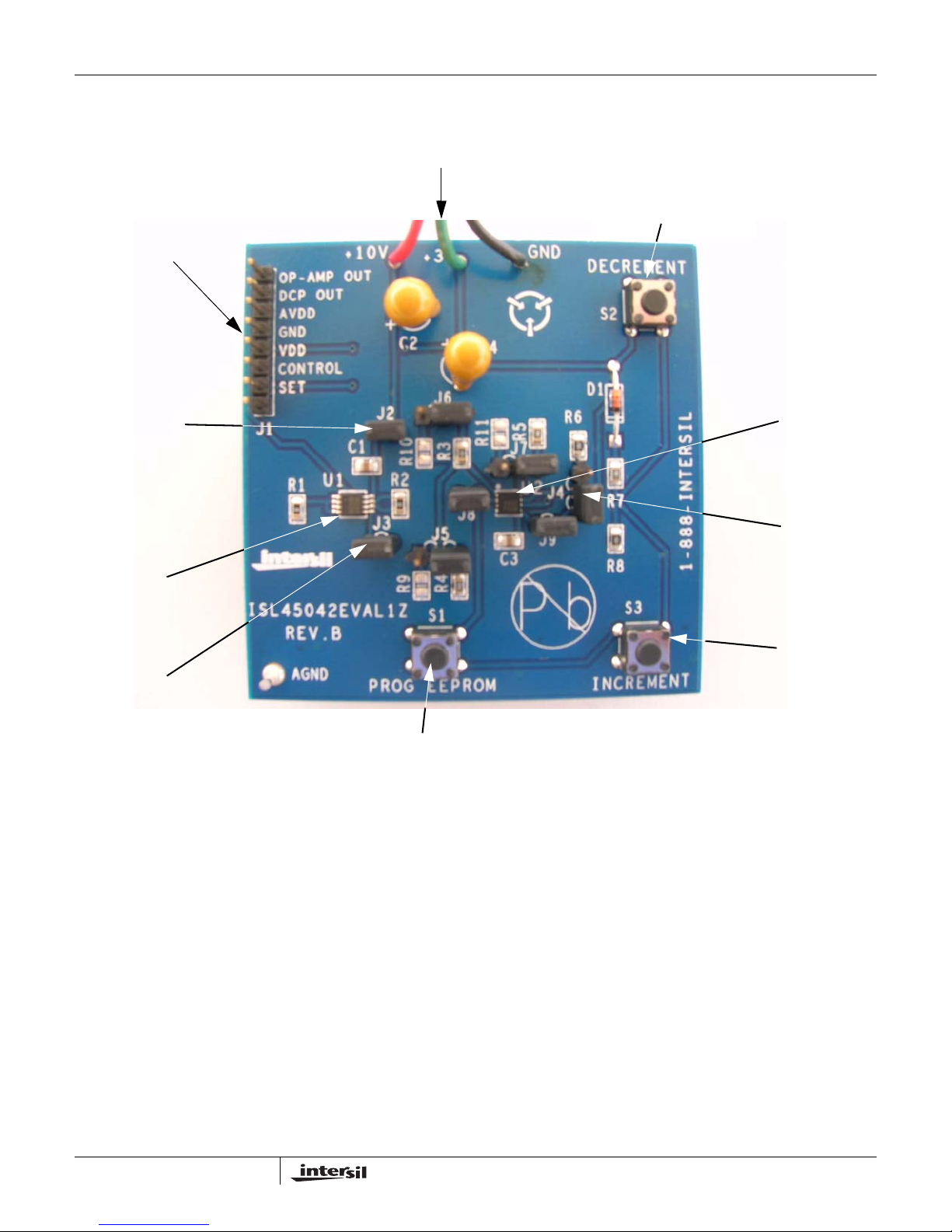
ISL45042EVAL1Z Picture
Application Note 1188
VDD, AVDD AND GND
CABLES
COUNTER DECREMENT
INPUT/OUTPUT
TEST--
HEADER
J2: EL5220
POWER
EL5220
OP AMP
J3: EL5220
+ INPUT
ISL45042
J4: CE HI/LO
JUMPER
COUNTER
INCREMENT
PROGRAM EEPROM
NOTES:
Jumpers J5, J6 and J7 allow user to choose different values of biasing and R
Jumpers J8 and J9 allow user to measure current draw of the ISL45042.
FIGURE 1. ISL45042 EVAL BOARD
2
SET
resistors.
AN1188.2
October 4, 2006
 Loading...