

®
ISL43681, ISL43741
Data Sheet September 2003
Low-Voltage, Single and Dual Supply,
8 to 1 Multiplexer and Differential 4 to 1
Multiplexer
The Intersil ISL43681 and ISL43741 devices are precision,
bidirectional, analog switches configured as an 8 channel and
a differential 4 channel multiplexer/demultiplexer. They are
designed to operate from a single +2V to +12V supply or from
a
±2V to ±6V supplies. The devices have an inhibit and inhibit
bar pin to simultaneously open all signal paths. The devices
also have a latch bar pin to lock in the last switch address.
ON resistance of 39Ω with a
±5V supply and 125Ω with a
+3.3V supply. Each switch can handle rail to rail analog
signals. The off-leakage current is only 0.1nA at +25
2.5nA at +85
o
C.
o
C or
All digital inputs have 0.8V to 2.4V logic thresholds, ensuring
TTL/CMOS logic compatibility when using a single 3.3V or
+5V supply or dual
±5V supplies.
The ISL43681 is a single 8 to 1 multiplexer device and the
ISL43741 is a diff 4 to 1 multiplexer device. Table 1
summarizes the performance of these parts.
TABLE 1. FEATURES AT A GLANCE
CONFIGURATION
±5V R
ON
±5V t
ON/tOFF
12V R
ON
12V t
ON/tOFF
5V R
ON
5V t
ON/tOFF
3.3V R
ON
3.3V t
ON/tOFF
Package 20 Ld 4x4 QFN
SINGLE 8:1 MUX,
DIFF 4:1 MUX
39Ω
32ns/18ns
32Ω
23ns/15ns
65Ω
38ns/19ns
125Ω
70ns/32ns
Related Literature
• Technical Brief TB363 “Guidelines for Handling and
Processing Moisture Sensitive Surface Mount Devices
(SMDs)”
• Application Note AN557 “Recommended Test Procedures
for Analog Switches”
• Application Note AN520 “CMOS Analog Multiplexers and
Switches; Specifications and Application Considerations.”
FN6053
Features
• Fully Specified at 3.3V, 5V, ±5V, and 12V Supplies for
10% Tolerances
• ON Resistance (R
• ON Resistance (R
•R
Matching Between Channels, VS = ±5V. . . . . . . . . <2Ω
ON
• Low Charge Injection, V
) Max, VS = ±4.5V. . . . . . . . . . . 50Ω
ON
) Max, VS = +3V . . . . . . . . . . . 155Ω
ON
= ±5V . . . . . . . . . . . . . 1pC (Max)
S
• Single Supply Operation. . . . . . . . . . . . . . . . . . . +2V to +12V
• Dual Supply Operation . . . . . . . . . . . . . . . . . . . . . ±2V to ±6V
• Fast Switching Action (V
. . . . . . . . . . . . . . . . . . . . . . . . . . . . . . . . . . . . 38ns
-t
ON
-t
. . . . . . . . . . . . . . . . . . . . . . . . . . . . . . . . . . . 19ns
OFF
= +5V)
S
• Guaranteed Max Off-leakage . . . . . . . . . . . . . . . . . . .2.5nA
• Guaranteed Break-Before-Make
• TTL, CMOS Compatible
Applications
• Battery Powered, Handheld, and Portable Equipment
• Communications Systems
-Radios
- Telecom Infrastructure
- ADSL, VDSL Modems
• Test Equipment
- Medical Ultrasound
- Magnetic Resonance Image
- CT and PET Scanners (MRI)
-ATE
- Electrocardiograph
• Audio and Video Signal Routing
• Various Circuits
- +3V/+5V DACs and ADCs
- Sample and Hold Circuits
- Operational Amplifier Gain Switching Networks
- High Frequency Analog Switching
- High Speed Multiplexing
- Integrator Reset Circuits
• Application Note AN1034 “Analog Switch and Multiplexer
Applications”
1
CAUTION: These devices are sensitive to electrostatic discharge; follow proper IC Handling Procedures.
1-888-INTERSIL or 321-724-7143
| Intersil (and design) is a registered trademark of Intersil Americas Inc.
Copyright © Intersil Americas Inc. 2003. All Rights Reserved.
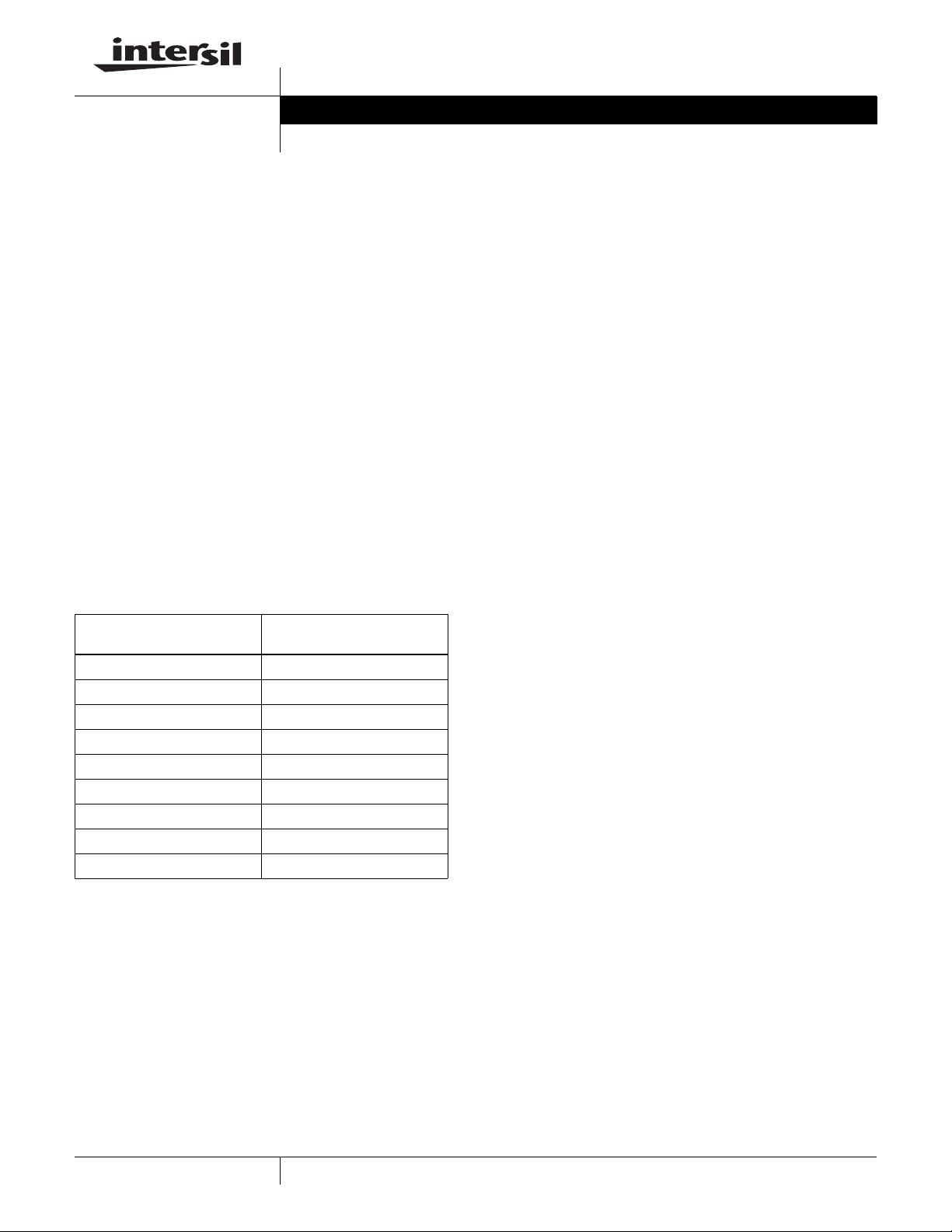
Pinouts
COM
NO7
NO5
EN
EN
ISL43681 (QFN)
TOP VIEW
NO3
NO1
N.C.
20 19 18 17 16
1
2
3
4
5
LOGIC
+V
NO2
ISL43681, ISL43741
ISL43741 (QFN)
TOP VIEW
A
NO1BNO0BN.C.
20 19 18 17 16
NO4
15
NO0
14
NO6
13
ADDC
12
ADDB
11
COM
NO3
NO2
EN
EN
1
B
2
B
3
B
4
5
LOGIC
+V
NO1
NO2
15
A
COM
14
13
12
11
NO0
NO3
ADDB
A
A
A
789106
-V
GND
N.C.
LE
ADDA
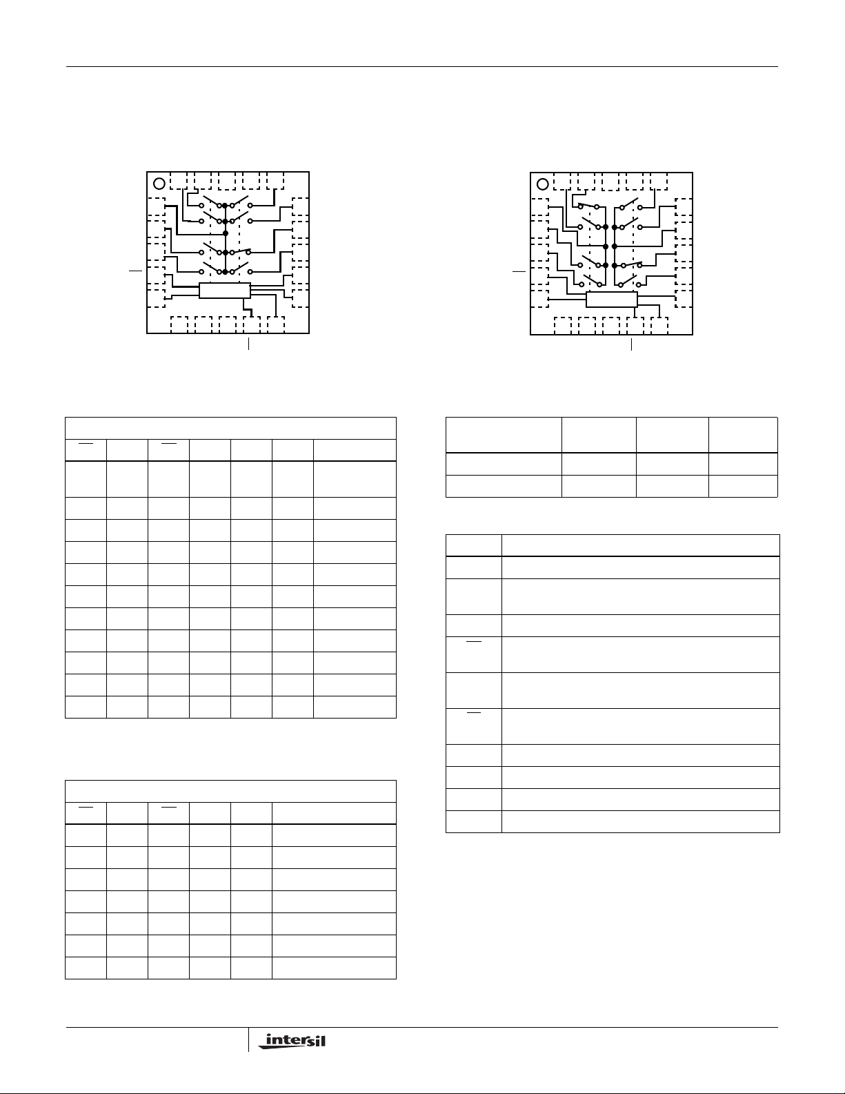
Truth Tables
ISL43681
LE
EN EN ADDC ADDB ADDA SWITCH ON
010XXXLast Switch
X0XXXXNONE
XX1XXXNONE
110000NO0
110001NO1
110010NO2
110011NO3
110100NO4
110101NO5
110110NO6
110111NO7
NOTE: Logic “0” ≤0.8V. Logic “1” ≥2.4V, with V+ between 2.7V and
10V. X = Don’t Care.
ISL43741
LE
EN EN ADDB ADDA SWITCH ON
0 1 0 X X Last Switch Selected
X 0 X X X NONE
XX1XXNONE
11000NO0
11001NO1
11010NO2
11011NO3
NOTE: Logic “0” ≤0.8V. Logic “1” ≥2.4V, with V+ between 2.7V and
10V. X = Don’t Care.
, NO0
A
, NO1
A
, NO2
A
, NO3
A
Selected
B
B
B
B
789106
-V
GND
N.C.
LE
ADDA
Ordering Information
PART NO.
(BRAND)
ISL43681IR (43681IR) -40 to 85 20 Ld QFN L20.4x4
ISL43741IR (43741IR) -40 to 85 20 Ld QFN L20.4x4
TEMP.
RANGE (
o
C) PACKAGE
PKG.
DWG. #
Pin Descriptions
PIN FUNCTION
V+ Positive Power Supply Input
V- Negative Power Supply Input. Connect to GND for
Single Supply Configurations.
GND Ground Connection
EN
Digital Control Input. Connect to GND for Normal
Operation. Connect to V+ to turn all switches off.
EN Digital Control Input. Connect to V+ for Normal
Operation. Connect to GND to turn all switches off.
LE
Digital Control Input. Connect to +V for Normal
Operation. Connect to GND to latch the last switch state.
COM Analog Switch Common Pin
NO Analog Switch Normally Open Pin
ADD Address Input Pin
N.C. No Internal Connection
2
ISL43681, ISL43741
Absolute Maximum Ratings Thermal Information
V+ to V- . . . . . . . . . . . . . . . . . . . . . . . . . . . . . . . . . . . . . . -0.3 to15V
V+ to GND . . . . . . . . . . . . . . . . . . . . . . . . . . . . . . . . . . . . -0.3 to15V
V- to GND . . . . . . . . . . . . . . . . . . . . . . . . . . . . . . . . . . . -15 to 0.3V
Input Voltages
LE
, EN, EN , NO, NC, ADD (Note 1) . . . . . . -0.3 to ((V+) + 0.3V)
Output Voltages
COM (Note 1). . . . . . . . . . . . . . . . . . . . . . . . -0.3 to ((V+) + 0.3V)
Continuous Current (Any Terminal). . . . . . . . . . . . . . . . . . . . ±30mA
Peak Current NO, NC, or COM
(Pulsed 1ms, 10% Duty Cycle, Max) . . . . . . . . . . . . . . . . ±100mA
ESD Rating
HBM ( Per Mil-STD-883, Method 3015.7) . . . . . . . . . . . . . >2.5kV
Operating Conditions
Temperature Range
ISL43681IR and ISl43741IR . . . . . . . . . . . . . . . . . . . -40
CAUTION: Stresses above those listed in “Absolute Maximum Ratings” may cause permanent damage to the device. This is a stress only rating and operation of the
device at these or any other conditions above those indicated in the operational sections of this specification is not implied.
NOTES:
1. Signals on NC, NO, COM, ADD, EN, EN
, or LE exceeding V+ or V- are clamped by internal diodes. Limit forward diode current to maximum
current ratings.
is measured with the component mounted on a high effective thermal conductivity test board with direct die attach. See Tech Brief TB379
2. θ
JA
for details.
o
C to 85oC
Thermal Resistance (Typical, Note 2) θ
(oC/W)
JA
20 Ld 4x4 QFN Package . . . . . . . . . . . . . . . . . . . . . 45
Maximum Junction Temperature (Plastic Package) . . . . . . . 150
Maximum Storage Temperature Range. . . . . . . . . . . . -65
o
C to 150oC
Maximum Lead Temperature (Soldering 10s). . . . . . . . . . . . 300
(Lead Tips Only)
o
o
C
C
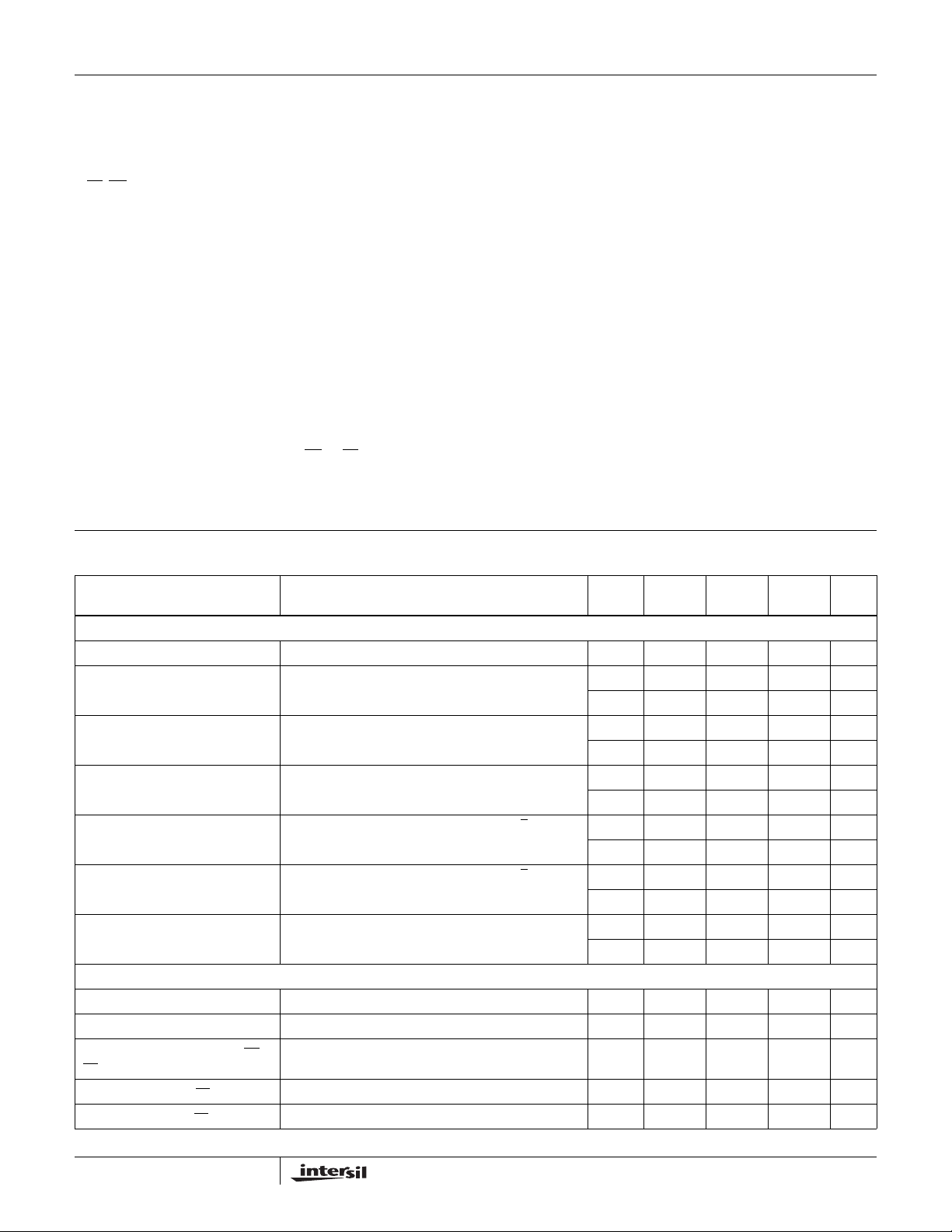
Electrical Specifications ±5V Supply Test Conditions: V
Unless Otherwise Specified
PARAMETER TEST CONDITIONS
ANALOG SWITCH CHARACTERISTICS
Analog Signal Range, V
ON Resistance, R
R
Matching Between Channels,
ON
∆R
ON
R
Flatness, R
ON
NO or NC OFF Leakage Current,
I
NO(OFF)
or I
NC(OFF)
COM OFF Leakage Current,
I
COM(OFF)
COM ON Leakage Current,
I
COM(ON)
DIGITAL INPUT CHARACTERISTICS
Input Voltage High, V
Input Voltage Low, V
Input Current, I
I
ENL
Input Current, I
Input Current, I
ADDH
ENH
ENL
ON
FLAT(ON)
INH
INL
, I
ADDL, IENH,
, I
LEH
, I
LEL
ANALOG
, V
ADDH
, V
ADDL
VS = ±4.5V, I
(See Figure 6)
VS = ±4.5V, I
VS = ±4.5V, I
(Note 6)
VS = ±5.5V, V
(Note 7)
VS = ±5.5V, V
(Note 7)
VS = ±5.5V, V
VS = ±5.5V, V
VS = ±5.5V, V
VS = ±5.5V, V
= 2mA, VNO or VNC = 3V
COM
= 2mA, VNO or VNC = 3V (Note 5) 25 - 1.3 4 Ω
COM
= 2mA, VNO or VNC = ±3V, 0V
COM
= ±4.5V, VNO or VNC = +4.5V
COM
= ±4.5V, VNO or VNC = +4.5V
COM
= VNO or VNC = ±4.5V (Note 7) 25 -0.1 0.002 0.1 nA
COM
, V
INH
INH
INH
= 0V or V+ Full -0.5 - 0.5 µA
ADD
, V
= 0V or V+ Full -1.5 - 1.5 µA
ADD
, V
= 0V or V+ Full -4 - 4 µA
ADD
= ±4.5V to ±5.5V, GND = 0V, V
SUPPLY
TEMP
o
(
C)
INH
(NOTE 4)
MIN TYP
= 2.4V, V
= 0.8V (Note 3),
INL
(NOTE 4)
MAX UNITS
Full V- - V+ V
25 - 44 50 Ω
Full - - 80 Ω
Full - - 6 Ω
25 - 7.5 9 Ω
Full - - 12 Ω
25 -0.1 0.002 0.1 nA
Full -2.5 - 2.5 nA
25 -0.1 0.002 0.1 nA
Full -2.5 - 2.5 nA
Full -2.5 - 2.5 nA
Full 2.4 - - V
Full - - 0.8 V
3
ISL43681, ISL43741
Electrical Specifications ±5V Supply Test Conditions: V
= ±4.5V to ±5.5V, GND = 0V, V
SUPPLY
= 2.4V, V
INH
= 0.8V (Note 3),
INL
Unless Otherwise Specified (Continued)
TEMP
PARAMETER TEST CONDITIONS
(NOTE 4)
o
(
C)
MIN TYP
(NOTE 4)
MAX UNITS
DYNAMIC CHARACTERISTICS
Enable Turn-ON Time, t
ON
Enable Turn-OFF Time, t
Address Transition Time, t
Break-Before-Make Time, t
Latch Setup Time, t
S
OFF
TRANSVS
BBM
VS = ±4.5V, VNO or VNC = ±3V, RL = 300Ω, CL = 35pF,
V
= 0 to 3 (See Figure 1)
IN
VS = ±4.5V, VNO or VNC = ±3V, RL = 300Ω, CL = 35pF,
V
= 0 to 3 (See Figure 1)
IN
= ±4.5V, VNO or VNC = ±3V, RL = 300Ω, CL = 35pF,
V
= 0 to 3 (See Figure 1)
IN
VS = ±5.5V, VNO or VNC = 3V, RL = 300Ω, CL = 35pF,
V
= 0 to 3V (See Figure 3)
IN
25 - 35 50 ns
Full - - 60 ns
25 - 22 35 ns
Full - - 40 ns
25 - 43 60 ns
Full - - 70 ns
Full 2 7 - ns
(See Figure 4) 25 25 - - ns
Full 35 - - ns
Latch Hold Time, t
H
(See Figure 4) 25 0 - - ns
Full 0 - - ns
Latch Pulse Width, t
WPW
(See Figure 4) 25 15 - - ns
Full 25 - ns
Charge Injection, Q C
NO/NC OFF Capacitance, C
COM OFF Capacitance, C
COM ON Capacitance, C
OFF
OFF
COM(ON)
OFF Isolation R
Crosstalk, (Note 8) (ISL43741 only) 25 - <-110 - dB
All Hostile Crosstalk, (Note 8)
= 1.0nF, VG = 0V, RG = 0Ω (See Figure 2) 25 - 0.3 1 pC
L
f = 1MHz, VNO or VNC = V
f = 1MHz, VNO or VNC = V
(See Figure 8)
f = 1MHz, VNO or VNC = V
(See Figure 8)
= 50Ω, CL = 15pF, f = 100kHz,
L
V
NOx
= 1V
(See Figures 5, 7 and 20)
RMS
= 0V (See Figure 8) 25 - 3 - pF
COM
COM
= 0V
ISL43681 25 - 21 - pF
ISL43741 25 - 12 - pF
COM
= 0V
ISL43681 25 - 26 - pF
ISL43741 25 - 18 - pF
25 - 92 - dB
25 - -105 - dB
(ISL43741 only)
POWER SUPPLY CHARACTERISTICS
Power Supply Range Full ±2-±6V
Positive Supply Current, I+ V
= ±5.5V, V
S
INH
, V
= 0V or V+, Switch On or Off Full -7 - 7 µA
ADD
Negative Supply Current, I- Full -1 - 1 µA
NOTES:
= Input logic voltage to configure the device in a given state.
3. V
IN
4. The algebraic convention, whereby the most negative value is a minimum and the most positive a maximum, is used in this data sheet.
5. ∆R
= RON (MAX) - RON (MIN).
ON
6. Flatness is defined as the difference between maximum and minimum value of on-resistance over the specified analog signal range.
o
7. Leakage parameter is 100% tested at high temp, and guaranteed by correlation at 25
C.
8. Between any two switches.
4
ISL43681, ISL43741
Electrical Specifications +12V Supply Test Conditions: V+ = +10.8V to +13.2V, GND = 0V, V
Unless Otherwise Specified
PARAMETER TEST CONDITIONS
ANALOG SWITCH CHARACTERISTICS
Analog Signal Range, V
ON Resistance, R
R
Matching Between Channels,
ON
∆R
ON
R
Flatness, R
ON
ON
FLAT(ON)
ANALOG
V+ = 10.8V, I
(See Figure 6)
V+ = 10.8V, I
V+ = 10.8V, I
(Note 6)
NO or NC OFF Leakage Current,
I
NO(OFF)
or I
NC(OFF)
COM OFF Leakage Current,
I
COM(OFF)
COM ON Leakage Current,
I
COM(ON)
V+ = 13.2V, V
(Note 7)
V+ = 13.2V, V
(Note 7)
V+ = 13.2V, V
or floating (Note 7)
DIGITAL INPUT CHARACTERISTICS
Input Voltage High, V
Input Voltage Low, V
Input Current, I
I
ENL
Input Current, I
Input Current, I
ADDH
ENH
ENL
, V
INH
, V
INL
, I
ADDL, IENH,
, I
LEH
, I
LEL
ADDH
ADDL
V+ = 13.2V, V
V+ = 13.2V, V
V+ = 13.2V, V
DYNAMIC CHARACTERISTICS
Enable Turn-ON Time, t
Enable Turn-OFF Time, t
Address Transition Time, t
ON
OFF
TRANS
Break-Before-Make Time Delay, t
Latch Setup Time, t
Latch Hold Time, t
Latch Pulse Width, t
S
H
WPW
Charge Injection, Q C
V+ = 10.8V, VNO or VNC = 10V, RL = 300Ω, CL = 35pF,
V
IN
V+ = 10.8V, VNO or VNC = 10V, RL = 300Ω, CL = 35pF,
V
IN
V+ = 10.8V, VNO or VNC = 10V, RL = 300Ω, CL = 35pF,
V
IN
V+ = 13.2V, RL = 300Ω, CL = 35pF, VNO or VNC = 10V,
D
V
IN
(See Figure 4) 25 25 - - ns
(See Figure 4) 25 0 - - ns
(See Figure 4) 25 15 - - ns
L
TEMP
= 1.0mA, VNO or VNC = 9V
COM
= 1.0mA, VNO or VNC = 9V (Note 5) 25 - 1.2 2 Ω
COM
= 1.0mA, VNO or VNC = 3V, 6V, 9V
COM
= 1V, 12V, VNO or VNC = 12V, 1V
COM
= 12V, 1V, VNO or VNC = 1V, 12V
COM
= 1V, 12V, VNO or VNC = 1V, 12V,
COM
, V
INH
INH
INH
= 0V or V+ Full -0.5 - 0.5 µA
ADD
, V
= 0V or V+ Full -1.5 - 1.5 µA
ADD
, V
= 0V or V+ Full -4 - 4 µA
ADD
= 0 to 4 (See Figure 1)
= 0 to 4 (See Figure 1)
= 0 to 4 (See Figure 1)
= 0 to 4 (See Figure 3)
= 1.0nF, VG = 0V, RG = 0Ω (See Figure 2) 25 - 2.7 5 pC
(NOTE 4)
o
(
C)
MIN TYP
Full 0 - V+ V
25 - 37 45 Ω
Full - - 55 Ω
Full - - 2 Ω
25 - 5 7 Ω
Full - - 7 Ω
25 -0.1 0.002 0.1 nA
Full -2.5 - 2.5 nA
25 -0.1 0.002 0.1 nA
Full -2.5 - 2.5 nA
25 -0.1 0.002 0.1 nA
Full -2.5 - 2.5 nA
Full 3.7 3.3 - V
Full - 2.7 0.8 V
25 - 24 40 ns
Full - - 45 ns
25 - 15 30 ns
Full - - 35 ns
25 - 27 50 ns
Full - - 55 ns
Full 2 5 - ns
Full 35 - - ns
Full 0 - - ns
Full 25 - - ns
INH
= 4V, V
= 0.8V (Note 3),
INL
(NOTE 4)
MAX UNITS
5
ISL43681, ISL43741
Electrical Specifications +12V Supply Test Conditions: V+ = +10.8V to +13.2V, GND = 0V, V
INH
= 4V, V
= 0.8V (Note 3),
INL
Unless Otherwise Specified (Continued)
TEMP
PARAMETER TEST CONDITIONS
OFF Isolation RL = 50Ω, CL = 15pF, f = 100kHz
Crosstalk, (Note 8), (ISL43741 only) 25 - <-110 - dB
(See Figure 5,7 and 20)
All Hostile Crosstalk, (Note 8)
(NOTE 4)
o
(
C)
MIN TYP
(NOTE 4)
MAX UNITS
25 - 92 - dB
25 - -105 - dB
(ISL43741 only)
NO or NC OFF Capacitance, C
COM OFF Capacitance,
C
COM(OFF)
COM ON Capacitance, C
COM(ON)
f = 1MHz, VNO or VNC = V
OFF
f = 1MHz, VNO or VNC = V
(See Figure 8)
f = 1MHz, VNO or VNC = V
(See Figure 8)
= 0V (See Figure 8) 25 - 3 - pF
COM
COM
= 0V
ISL43681 25 - 21 - pF
ISL43741 25 - 12 - pF
COM
= 0V
ISL43681 25 - 26 - pF
ISL43741 25 - 18 - pF
POWER SUPPLY CHARACTERISTICS
Power Supply Range Full 2 - 12 V
Positive Supply Current, I+ V+ = 13.2V, V
Positive Supply Current, I- Full -1 - 1 µA
off
Electrical Specifications 5V Supply Test Conditions: V+ = +4.5V to +5.5V, V- = GND = 0V, V
PARAMETER TEST CONDITIONS
, V
INH
= 0V or V+, all channels on or
ADD
Unless Otherwise Specified
Full -7 - 7 µA
TEMP
o
C)
(
= 2.4V, V
INH
MIN
(NOTE 4) TYP
= 0.8V (Note 3),
INL
MAX
(NOTE 4)UNITS
ANALOG SWITCH CHARACTERISTICS
Analog Signal Range, V
ON Resistance, R
R
Matching Between Channels,
ON
∆R
ON
R
Flatness, R
ON
ANALOG
ON
FLAT(ON)
NO or NC OFF Leakage Current,
I
NO(OFF)
or I
NC(OFF)
COM OFF Leakage Current,
I
COM(OFF)
COM ON Leakage Current,
I
COM(ON)
V+ = 4.5V, I
COM
(See Figure 6)
V+ = 4.5V, I
V+ = 4.5V, I
(Note 6)
COM
COM
V+ = 5.5V, V
(Note 7)
V+ = 5.5V, V
(Note 7)
V+ = 5.5V, V
= 1.0mA, VNO or VNC = 3.5V
= 1.0mA, VNO or VNC = 3V (Note 5) 25 - 2.2 4 Ω
= 1.0mA, VNO or VNC = 1V, 2V, 3V
= 1V, 4.5V, VNO or VNC = 4.5V, 1V
COM
= 1V, 4.5V, VNO or VNC = 4.5V, 1V
COM
= VNO or V
COM
4.5V (Note 7) 25 -0.1 0.002 0.1 nA
NC =
Full 0 - V+ V
25 - 81 90 Ω
Full - - 120 Ω
Full - - 6 Ω
25 - 11.5 17 Ω
Full - - 24 Ω
25 -0.1 0.002 0.1 nA
Full -2.5 - 2.5 nA
25 -0.1 0.002 0.1 nA
Full -2.5 - 2.5 nA
Full -2.5 - 2.5 nA
DIGITAL INPUT CHARACTERISTICS
Input Voltage High, V
Input Voltage Low, V
Input Current, I
I
ENL
Input Current, I
Input Current, I
ADDH
ENH
ENL
, V
INH
, V
INL
, I
ADDL, IENH,
, I
LEH
, I
LEL
ADDH
ADDL
V+ = 5.5V, V
V+ = 5.5V, V
V+ = 5.5V, V
INH
INH
INH
Full 2.4 - - V
Full - - 0.8 V
, V
= 0V or V+ Full -0.5 - 0.5 µA
ADD
, V
= 0V or V+ Full -1.5 - 1.5 µA
ADD
, V
= 0V or V+ Full -4 - 4 µA
ADD
6

ISL43681, ISL43741
Electrical Specifications 5V Supply Test Conditions: V+ = +4.5V to +5.5V, V- = GND = 0V, V
= 2.4V, V
INH
= 0.8V (Note 3),
INL
Unless Otherwise Specified (Continued)
PARAMETER TEST CONDITIONS
TEMP
o
(
C)
MIN
(NOTE 4) TYP
MAX
(NOTE 4)UNITS
DYNAMIC CHARACTERISTICS
Enable Turn-ON Time, t
ON
Enable Turn-OFF Time, t
Address Transition Time, t
Break-Before-Make Time, t
Latch Setup Time, t
S
OFF
TRANS
BBM
V+ = 4.5V, VNO or VNC = 3V, RL = 300Ω, CL = 35pF,
V
= 0 to 3V (See Figure 1)
IN
V+ = 4.5V, VNO or VNC = 3V, RL = 300Ω, CL = 35pF,
V
= 0 to 3V (See Figure 1)
IN
V+ = 4.5V, VNO or VNC = 3V, RL = 300Ω, CL = 35pF,
V
= 0 to 3V (See Figure 1)
IN
V+ = 5.5V, VNO or VNC = 3V, RL = 300Ω, CL = 35pF,
V
= 0 to 3V (See Figure 3)
IN
25 - 43 60 ns
Full - - 70 ns
25 - 20 35 ns
Full - - 40 ns
25 - 51 70 ns
Full - - 85 ns
Full 2 9 - ns
(See Figure 4) 25 25 - - ns
Full 35 - - ns
Latch Hold Time, t
H
(See Figure 4) 25 0 - - ns
Full 0 - - ns
Latch Pulse Width, t
WPW
(See Figure 4) 25 15 - - ns
Full 25 - - ns
Charge Injection, Q C
OFF Isolation R
Crosstalk, (Note 8), (ISL43741 only) 25 - <-110 - dB
All Hostile Crosstalk, (Note 8),
= 1.0nF, VG = 0V, RG = 0Ω (See Figure 2) 25 - 0.6 1.5 pC
L
= 50Ω, CL = 15pF, f = 100kHz,
L
V
NOx
= 1V
(See Figures 5, 7 and 20)
RMS
25 - 92 - dB
25 - -105 1.5 dB
(ISL43741 only)
POWER SUPPLY CHARACTERISTICS
Power Supply Range Full 2 - 12 V
Positive Supply Current, I+ V+ = 5.5V, V- = 0V, V
Positive Supply Current, I- Full -1 - 1 µA
Switch On or Off
INH
, V
ADD
= 0V or V+,
Full -7 - 7 µA
Electrical Specifications 3.3V Supply Test Conditions: V+ = +3.0V to +3.6V, V- = GND = 0V, V
Unless Otherwise Specified
PARAMETER TEST CONDITIONS
ANALOG SWITCH CHARACTERISTICS
Analog Signal Range, V
ON Resistance, R
R
Matching Between Channels,
ON
∆R
ON
R
Flatness, R
ON
ON
FLAT(ON)
ANALOG
V+ = 3.0V, I
(See Figure 6)
V+ = 3.0V, I
V+ = 3.0V, I
(Note 6)
NO or NC OFF Leakage Current,
I
NO(OFF)
or I
NC(OFF)
V+ = 3.6V, V
(Note 7)
7
TEMP
o
(
C)
Full 0 - V+ V
= 1.0mA, VNO or VNC = 1.5V
COM
25 - 135 155 Ω
Full - - 200 Ω
= 1.0mA, VNO or VNC = 1.5V (Note 5) 25 - 3.4 8 Ω
COM
Full - - 10 Ω
= 1.0mA, VNO or VNC = 0.5V, 1V, 2V
COM
25 - 34 40 Ω
Full - - 50 Ω
= 0V, 4.5V, VNO or VNC = 3V, 1V
COM
25 -0.1 0.002 0.1 nA
Full -2.5 - 2.5 nA
MIN
(NOTE 4) TYP
= 2.4V, V
INH
= 0.8V (Note 3),
INL
MAX
(NOTE 4)UNITS

ISL43681, ISL43741
Electrical Specifications 3.3V Supply Test Conditions: V+ = +3.0V to +3.6V, V- = GND = 0V, V
= 2.4V, V
INH
= 0.8V (Note 3),
INL
Unless Otherwise Specified (Continued)
PARAMETER TEST CONDITIONS
COM OFF Leakage Current,
I
COM(OFF)
COM ON Leakage Current,
I
COM(ON)
V+ = 3.6V, V
(Note 7)
V+ = 3.6V, V
= 0V, 4.5V, VNO or VNC = 3V, 1V
COM
= VNO or V
COM
3V (Note 7 ) 25 -0.1 0.002 0.1 nA
NC =
TEMP
o
(
C)
25 -0.1 0.002 0.1 nA
Full -2.5 - 2.5 nA
Full -2.5 - 2.5 nA
MIN
(NOTE 4) TYP
MAX
(NOTE 4)UNITS
DIGITAL INPUT CHARACTERISTICS
Input Voltage High, V
Input Voltage Low, V
Input Current, I
I
ENL
Input Current, I
Input Current, I
ADDH
ENH
ENL
, V
INH
ADDH
, V
INL
ADDL
, I
ADDL, IENH,
, I
V+ = 3.6V, V
LEH
, I
LEL
V+ = 3.6V, V
V+ = 3.6V, V
INH
INH
INH
Full 2.4 - - V
Full - - 0.8 V
, V
= 0V or V+ Full -0.5 - 0.5 µA
ADD
, V
= 0V or V+ Full -1.5 - 1.5 µA
ADD
, V
= 0V or V+ Full -4 - 4 µA
ADD
DYNAMIC CHARACTERISTICS
Enable Turn-ON Time, t
ON
Enable Turn-OFF Time, t
Address Transition Time, t
Break-Before-Make Time, t
Latch Setup Time, t
S
OFF
TRANS
BBM
V+ = 3.0V, VNO or VNC = 1.5V, RL = 300Ω, CL = 35pF,
V
= 0 to 3V (See Figure 1)
IN
V+ = 3.0V, VNO or VNC = 1.5V, RL = 300Ω, CL = 35pF,
V
= 0 to 3V (See Figure 1)
IN
V+ = 3.0V, VNO or VNC = 1.5V, RL = 300Ω, CL = 35pF,
V
= 0 to 3V (See Figure 1)
IN
V+ = 3.6V, VNO or VNC = 1.5V, RL = 300Ω, CL = 35pF,
V
= 0 to 3V (See Figure 3)
IN
25 - 82 100 ns
Full - - 120 ns
25 - 37 50 ns
Full - - 60 ns
25 - 96 120 ns
Full - - 145 ns
Full 3 13 - ns
(See Figure 4) 25 50 - - ns
Full 60 - - ns
Latch Hold Time, t
H
(See Figure 4) 25 0 - - ns
Full 0 - - ns
Latch Pulse Width, t
WPW
(See Figure 4) 25 30 - - ns
Full 40 - - ns
Charge Injection, Q C
OFF Isolation R
Crosstalk, (Note 8), (ISL43741 only) 25 - <-110 - dB
All Hostile Crosstalk, (Note 8),
= 1.0nF, VG = 0V, RG = 0Ω (See Figure 2) 25 - 0.3 1 pC
L
= 50Ω, CL = 15pF, f = 100kHz,
L
V
or VNC = 1V
NO
(See Figures 5, 7 and 20)
RMS
25 - 92 - dB
25 - -105 - dB
(ISL43741 only)
POWER SUPPLY CHARACTERISTICS
Power Supply Range Full 2 - 12 V
, V
Positive Supply Current, I+ V+ = 3.6V, V- = 0V, V
Positive Supply Current, I- Full -1 - 1 µA
Switch On or Off
INH
= 0V or V+,
ADD
Full -7 - 7 µA
8

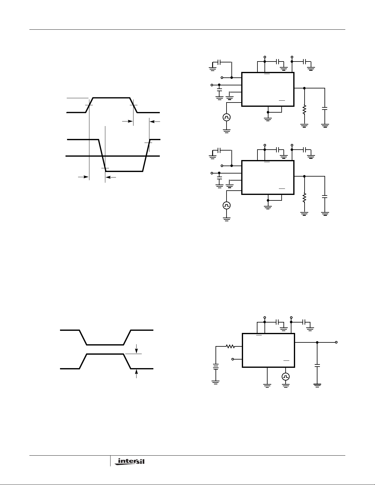
Test Circuits and Waveforms
ISL43681, ISL43741
V+
C
V-
C
C
tr < 20ns
< 20ns
t
f
90%
LOGIC
INPUT
SWITCH
OUTPUT
3V
0V
VNO0
0V
t
OFF
50%
90%
t
ON
V
OUT
Logic input waveform is inverted for switches that have the opposite
logic sense.
FIGURE 1A. ENABLE t
ON/tOFF
MEASUREMENT POINTS
EN, LE
V+
LOGIC
INPUT
V+
LOGIC
INPUT
C
NO0
NO1-NO7
EN
V+
EN, LE
NO0
x
-NO3
NO1
x
EN
GND
x
GND
Repeat test for other switches. C
capacitance.
V
OUT
V
=
(NO or NC)
FIGURE 1B. ENABLE t
ISL43681
COM
ADDA-C
V-
C
ISL43741
COM
x
ADDA-B
includes fixture and stray
L
------------------------------
RLR
ON/tOFF
V
OUT
RL
300Ω
C
V
OUT
RL
300Ω
R
L
+
ON()
TEST CIRCUIT
C
L
35pF
CL
35pF
9
ISL43681, ISL43741
Test Circuits and Waveforms (Continued)
LOGIC
INPUT
SWITCH
OUTPUT
3V
0V
VNO0
0V
VNO
50%
t
TRANS
V
OUT
X
t
TRANS
10%
tr < 20ns
< 20ns
t
f
90%
Logic input waveform is inverted for switches that have the opposite
logic sense.
FIGURE 1C. ADDRESS t
MEASUREMENT POINTS
TRANS
FIGURE 1. SWITCHING TIMES
EN, LE
NO0
NO7
NO1-NO6
EN, LE
x
x
V+
GND
V+
x
GND
V-
LOGIC
INPUT
V-
LOGIC
INPUT
C
V+
C
ADDA-C
C
V+
C
NO0
NO3
NO1x-NO2
ADDA-B
Repeat test for other switches. C
capacitance.
V
OUT
V
=
(NO or NC)
FIGURE 1D. ADDRESS t
V-
C
ISL43681
COM
EN
C
ISL43741
COM
EN
includes fixture and stray
L
------------------------------
RLR
TRANS
C
V
OUT
RL
300Ω
V-
C
V
x
R
+
OUT
RL
300Ω
L
ON()
TEST CIRCUIT
C
L
35pF
CL
35pF
OUT
OFF
Q = ∆V
OUT
x C
ON
L
LOGIC
INPUT
SWITCH
OUTPUT
V
FIGURE 2A. Q MEASUREMENT POINTS
10
3V
0V
∆V
OFF
OUT
FIGURE 2. CHARGE INJECTION
G
EN, LE
NO or NC
ADDX
R
0Ω
V
G
Repeat test for other switches.
FIGURE 2B. Q TEST CIRCUIT
V+
GND
V-
EN
LOGIC
INPUT
C
V
OUT
C
L
1nF
C
COM

ISL43681, ISL43741
Test Circuits and Waveforms (Continued)
LOGIC
INPUT
SWITCH
OUTPUT
V
OUT
3V
0V
0V
t
BBM
tr < 20ns
t
< 20ns
f
80%
V+
LOGIC
INPUT
V+
LOGIC
INPUT
C
COM
ISL43681
EN
C
COM
EN
V-
C
V
OUT
R
L
300Ω
V-
C
V
x
OUT
R
300Ω
L
C
35pF
C
35pF
L
L
V+
C
EN, LE
NO0-NO7
ADDA-C
GND
V+
C
EN, LE
NO0
-NO3
x
x
ADDA-B
ISL43741
GND
FIGURE 3A. t
MEASUREMENT POINTS
BBM
Repeat test for other switches. C
capacitance.
FIGURE 3. BREAK-BEFORE-MAKE TIME
FIGURE 3B. t
includes fixture and stray
L
TEST CIRCUIT
BBM
11

ISL43681, ISL43741
Test Circuits and Waveforms (Continued)
tr < 20ns
< 20ns
t
f
50%50%
t
H
50%
tON, t
OFF
90%
LOGIC
INPUT
LE
LOGIC
INPUT
ADD
X
SWITCH
OUTPUT
VNO
3V
0V
3V
0V
0V
t
MPW
50%
t
H
X
50%
V
OUT
t
S
Logic input waveform is inverted for switches that have the opposite
logic sense.
V+
C
EN
ADDA-C
LOGIC
INPUT
LOGIC
INPUT
LOGIC
INPUT
LOGIC
INPUT
LE
V+
EN
ADDA-B
LE
GND
C
GND
Repeat test for other switches. C
capacitance.
V
OUT
V
=
(NO or NC)
V-
C
NO1-NO7
NO0
ISL43681
EN
V-
NO1
x
ISL43741
EN
includes fixture and stray
L
COM
C
-NO3
x
NO0
x
COM
R
------------------------------
RLR
+
V
OUT
V
OUT
L
ON()
RL
300Ω
RL
300Ω
C
V+
CL
35pF
C
V+
CL
35pF
FIGURE 4A. LATCH t
SIGNAL
GENERATOR
ANALYZER
R
L
FIGURE 5. OFF ISOLATION TEST CIRCUIT
S
, tH, t
MEASUREMENT POINTS
MPW
V+
C
EN, LE
NO or NC
ADDX
COM
GND
EN
FIGURE 4B. LATCH t
FIGURE 4. LATCH SETUP AND HOLD TIMES
V-
C
RON = V1/1mA
V
NX
0V or V+
0V or V+
1mA
V
1
FIGURE 6. R
, tH, t
S
MPW
V+
EN, LE
NO or NC
COM
GND
TEST CIRCUIT
ON
TEST CIRCUIT
V-
C
ADDX
EN
C
0V or V+
12

ISL43681, ISL43741
Test Circuits and Waveforms (Continued)
C
COM
EN
V-
C
50Ω
A
B
N.C.
SIGNAL
GENERATOR
ANALYZER
V+
EN, LE
NOA or NC
0V or V+
R
L
FIGURE 7. CROSSTALK TEST CIRCUIT
ADDX
COM
B
A
ISL43741
NOB or NC
GND
Detailed Description
The ISL43681 and ISL43741 multiplexers offer precise
switching capability from a bipolar
to 12V supply with low on-resistance (39Ω) and high speed
operation (t
=38ns, t
ON
OFF
They have an inhibit and inhibit bar pin to simultaneously
open all signal paths. They also have a latch bar pin to lock
in the last switch address.
The devices are especially well suited for applications using
±5V supplies. With ±5V supplies the performance (R
Leakage, Charge Injection, etc.) is best in class.
High frequency applications also benefit from the wide
bandwidth, and the very high off isolation and crosstalk
rejection.
±2V to ±6V or a single 2V
= 19ns) with dual 5V supplies.
,
ON
C
ADDX
EN
V-
0V or V+
C
EN, LE
NO or NC
IMPEDANCE
ANALYZER
COM
FIGURE 8. CAPACITANCE TEST CIRCUIT
V+
GND
diodes can be added in series with the supply pins to provide
overvoltage protection for all pins (see Figure 9). These
additional diodes limit the analog signal from 1V below V+ to
1V above V-. The low leakage current performance is
unaffected by this approach, but the switch resistance may
increase, especially at low supply voltages.
OPTIONAL
PROTECTION
RESISTOR
FOR LOGIC
INPUTS
1kΩ
LOGIC
V
NO or NC
OPTIONAL PROTECTION
DIODE
V+
V
COM
Supply Sequencing And Overvoltage Protection
With any CMOS device, proper power supply sequencing is
required to protect the device from excessive input currents
which might permanently damage the IC. All I/O pins contain
ESD protection diodes from the pin to V+ and to V- (see
Figure 9). To prevent forward biasing these diodes, V+ and
V- must be applied before any input signals, and input signal
voltages must remain between V+ and V-. If these conditions
cannot be guaranteed, then one of the following two
protection methods should be employed.
Logic inputs can easily be protected by adding a 1kΩ
resistor in series with the input (see Figure 9). The resistor
limits the input current below the threshold that produces
permanent damage, and the sub-microamp input current
produces an insignificant voltage drop during normal
operation.
This method is not applicable for the signal path inputs.
Adding a series resistor to the switch input defeats the
purpose of using a low R
switch, so two small signal
ON
13
V-
OPTIONAL PROTECTION
DIODE
FIGURE 9. INPUT OVERVOLTAGE PROTECTION
Power-Supply Considerations
The ISL43681 and ISL43741 construction is typical of most
CMOS analog switches, in that they have three supply pins:
V+, V-, and GND. V+ and V- drive the internal CMOS
switches and set their analog voltage limits, so there are no
connections between the analog signal path and GND.
Unlike switches with a 13V maximum supply voltage, the
ISL43681 and ISL43741 15V maximum supply voltage
provides plenty of room for the 10% tolerance of 12V
supplies (
overshoot and noise spikes.
This family of switches performs equally well when operated
with bipolar or single voltage supplies.The minimum
±6V or 12V single supply), as well as room for
ISL43681, ISL43741
recommended supply voltage is 2V or ±2V. It is important to
note that the input signal range, switching times, and onresistance degrade at lower supply voltages. Refer to the
electrical specification tables and Typical Performance
curves for details.
V+ and GND power the internal logic (thus setting the digital
switching point) and level shifters. The level shifters convert
the logic levels to switched V+ and V- signals to drive the
analog switch gate terminals.
Logic-Level Thresholds
V+ and GND power the internal logic stages, so V- has no
affect on logic thresholds. This switch family is TTL
compatible (0.8V and 2.4V) over a V+ supply range of 2.7V
to 10V. At 12V the V
level is about 3.3V. This is still below
IH
the CMOS guaranteed high output minimum level of 4V, but
noise margin is reduced. For best results with a 12V supply,
use a logic family that provides a V
greater than 4V.
OH
The digital input stages draw supply current whenever the
digital input voltage is not at one of the supply rails. Driving
the digital input signals from GND to V+ with a fast transition
time minimizes power dissipation.
High-Frequency Performance
In 50Ω systems, signal response is reasonably flat even past
100MHz (see Figures 18 and 19). Figures 18 and 19 also
illustrates that the frequency response is very consistent
over varying analog signal levels.
An OFF switch acts like a capacitor and passes higher
frequencies with less attenuation, resulting in signal feed
through from a switch’s input to its output. Off Isolation is the
resistance to this feed through, while Crosstalk indicates the
amount of feed through from one switch to another. Figure
20 details the high Off Isolation and Crosstalk rejection
provided by this family. At 10MHz, Off Isolation is about
55dB in 50Ω systems, decreasing approximately 20dB per
decade as frequency increases. Higher load impedances
decrease Off Isolation and Crosstalk rejection due to the
voltage divider action of the switch OFF impedance and the
load impedance.
Leakage Considerations
Reverse ESD protection diodes are internally connected
between each analog-signal pin and both V+ and V-. One
of these diodes conducts if any analog signal exceeds V+
or V-.
Virtually all the analog leakage current comes from the ESD
diodes to V+ or V-. Although the ESD diodes on a given
signal pin are identical and therefore fairly well balanced,
they are reverse biased differently. Each is biased by either
V+ or V- and the analog signal. This means their leakages
will vary as the signal varies. The difference in the two diode
leakages to the V+ and V- pins constitutes the analog-signalpath leakage current. All analog leakage current flows
between each pin and one of the supply terminals, not to the
other switch terminal. This is why both sides of a given
switch can show leakage currents of the same or opposite
polarity. There is no connection between the analog signal
paths and GND.
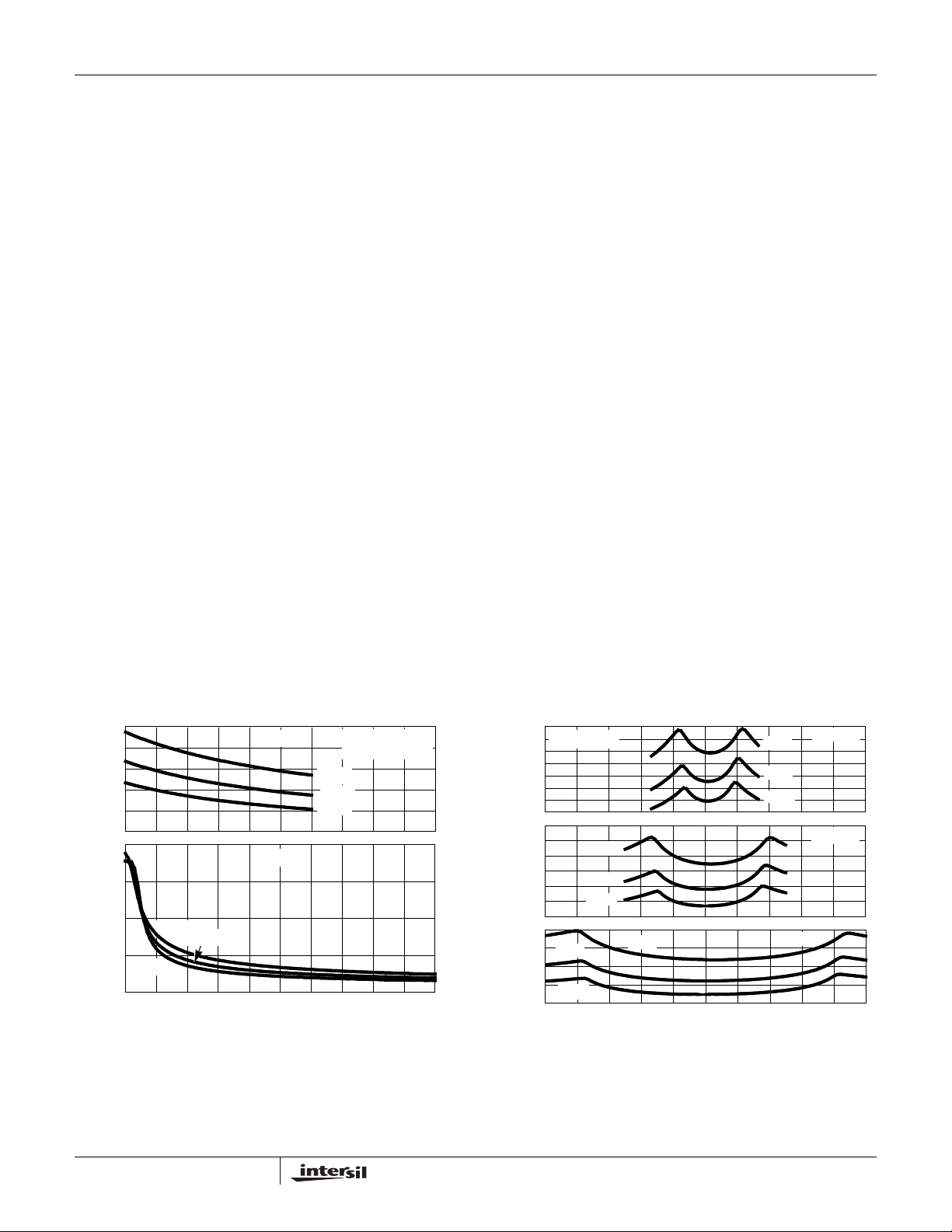
Typical Performance Curves T
70
60
50
40
30
20
400
(Ω)
ON
R
300
200
100
85oC
25oC
-40oC
0
2
4681012357911
V- = -5V
V- = 0V
V+ (V)
A
85oC
25oC
-40oC
FIGURE 10. ON RESISTANCE vs SUPPLY VOLTAGE
= 25oC, Unless Otherwise Specified
V
COM
I
COM
= (V+) - 1V
= 1mA
120
110
100
90
80
70
60
50
90
80
70
(Ω)
60
ON
50
R
40
30
60
50
40
30
20
FIGURE 11. ON RESISTANCE vs SWITCH VOLTAGE
I
= 1mA
COM
85oC
25oC
-40oC
25oC
-40oC
-5 -3 -1 1 3 5
-4 -2 0 2 4
85oC
V
COM
(V)
85oC
25oC
-40oC
VS = ±2V
VS = ±3V
VS = ±5V
14

ISL43681, ISL43741
Typical Performance Curves T
225
200
175
150
125
100
75
160
140
(Ω)
120
ON
100
R
80
60
100
90
80
70
60
50
40
024
85oC
25oC
135
V+ = 5V
V
COM
(V)
= 25oC, Unless Otherwise Specified (Continued)
A
I
= 1mA
COM
85oC
25oC
-40oC
V- = 0V
85oC
25oC
-40oC
V+ = 2.7V
V- = 0V
V+ = 3.3V
V- = 0V
-40oC
60
I
55
50
45
40
(Ω)
ON
R
35
30
25
20
024681012
V+ = 12V
V- = 0V
25oC
V
(V)
COM
85oC
COM
-40oC
= 1mA
FIGURE 12. ON RESISTANCE vs SWITCH VOLTAGE FIGURE 13. ON RESISTANCE vs SWITCH VOLTAGE
500
400
-40oC
300
200
100
(ns)
ON
t
25oC
25oC
85oC
-40oC
0
250
200
85oC
150
100
50
-40oC
0
24681012357911
25oC
V- = -5V
V- = 0V
V+ (V)
V
COM
= (V+) - 1V
200
-40oC
150
100
(ns)
100
OFF
t
25oC
25oC
50
-40oC
0
80
60
40
20
0
24681012
85oC
85oC
25oC
-40oC
357911
V- = -5V
V- = 0V
V+ (V)
V
COM
= (V+) - 1V
FIGURE 14. ENABLE TURN - ON TIME vs SUPPLY VOLTAGE FIGURE 15. ENABLE TURN - OFF TIME vs SUPPLY VOLTAGE
300
250
200
(ns)
150
RANS
t
100
50
0
35791113
24681012
25oC
85oC
-40oC
V+ (V)
V
COM
= (V+) - 1V
V- = 0V
FIGURE 16. ADDRESS TRANS TIME vs SINGLE SUPPLY
VOLTAGE
15
250
200
150
(ns)
RANS
t
100
50
0
23456
25oC
85oC
-40oC
V± (V)
V
COM
= (V+) - 1V
FIGURE 17. ADDRESS TRANS TIME vs DUAL SUPPLY
VOLTAGE

ISL43681, ISL43741
Typical Performance Curves T
VS = ±5V
3
GAIN
0
-3
NORMALIZED GAIN (dB)
PHASE
RL = 50Ω
1 10 100 600
FREQUENCY (MHz)
VIN = 0.2V
ISL43681
ISL43681
ISL43741
= 25oC, Unless Otherwise Specified (Continued)
A
P-P
FIGURE 18. FREQUENCY RESPONSE
-10
V+ = 3V to 12V or
-20
VS = ±2V to ±5V
RL = 50Ω
-30
-40
-50
-60
-70
CROSSTALK (dB)
-80
ISOLATION
CROSSTALK
to 5V
P-P
ISL43741
0
45
90
135
180
10
20
30
40
50
60
70
80
VS = ±3V
3
GAIN
0
-3
NORMALIZED GAIN (dB)
PHASE
PHASE (DEGREES)
RL = 50Ω
1 10 100 600
FREQUENCY (MHz)
VIN = 0.2V
ISL43681
ISL43681
ISL43741
to 4V
P-P
ISL43741
P-P
0
45
90
135
180
PHASE (DEGREES)
FIGURE 19. FREQUENCY RESPONSE
3
2
1
0
-1
Q (pC)
OFF ISOLATION (dB)
-2
V+ = 3.3V
V- = 0V
VS = ±5V
V+ = 5V
V- = 0V
V+ = 12V
V- = 0V
-90
-100
ALL HOSTILE CROSSTALK
-110
1k 100k 1M 100M 500M10k 10M
FREQUENCY (Hz)
FIGURE 20. CROSSTALK AND OFF ISOLATION
Die Characteristics
SUBSTRATE POTENTIAL (POWERED UP):
GND
TRANSISTOR COUNT:
ISL43681: 193
ISL43741: 193
PROCESS:
Si Gate CMOS
16
90
100
110
-3
-4
-5 0 5 10 12
-2.5 2.5 7.5
V
(V)
COM
FIGURE 21. CHARGE INJECTION vs SWITCH VOLTAGE

ISL43681, ISL43741
Quad Flat No-Lead Plastic Package (QFN)
Micro Lead Frame Plastic Package (MLFP)
L20.4x4
20 LEAD QUAD FLAT NO-LEAD PLASTIC PACKAGE
(COMPLIANT TO JEDEC MO-220VGGD-1 ISSUE C)
MILLIMETERS
SYMBOL
A 0.80 0.90 1.00 A1 - - 0.05 A2 - - 1.00 9
A3 0.20 REF 9
b 0.18 0.23 0.30 5, 8
D 4.00 BSC D1 3.75 BSC 9
D2 1.95 2.10 2.25 7, 8
E 4.00 BSC E1 3.75 BSC 9
E2 1.95 2.10 2.25 7, 8
e 0.50 BSC k0.25 - - L 0.35 0.60 0.75 8
L1 - - 0.15 10
N202
Nd 5 3
Ne 5 5 3
P- -0.609
θ --129
NOTES:
1. Dimensioning and tolerancing conform to ASME Y14.5-1994.
2. N is the number of terminals.
3. Nd and Ne refer to the number of terminals on each D and E.
4. All dimensions are in millimeters. Angles are in degrees.
5. Dimension b applies to the metallized terminal and is measured
between 0.15mm and 0.30mm from the terminal tip.
6. The configuration of the pin #1 identifier is optional, but must be
located within the zone indicated. The pin #1 identifier may be
either a mold or mark feature.
7. Dimensions D2 and E2 are for the exposed pads which provide
improved electrical and thermal performance.
8. Nominal dimensions are provided to assist with PCB Land Pattern
Design efforts, see Intersil Technical Brief TB389.
9. Features and dimensions A2, A3, D1, E1, P & θ are present when
Anvil singulation method is used and not present for saw
singulation.
10. Depending on the method of lead termination at the edge of the
package, a maximum 0.15mm pull back (L1) maybe present. L
minus L1 to be equal to or greater than 0.3mm.
NOTESMIN NOMINAL MAX
Rev. 1 10/02
All Intersil U.S. products are manufactured, assembled and tested utilizing ISO9000 quality systems.
Intersil Corporation’s quality certifications can be viewed at www.intersil.com/design/quality
Intersil products are sold by description only. Intersil Corporation reserves the right to make changes in circuit design, software and/or specifications at any time without
notice. Accordingly, the reader is cautioned to verify that data she ets are current before placin g orders. Information furn ished by Intersil is believed to be accurate and
reliable. However, no responsibility is assumed by Intersil or its subsidiaries for its use; nor for any infringements of patents or other rights of third parties which may result
from its use. No license is granted by implication or othe rwise under any patent or patent rights of Intersil or its subsidia ries.
For information regarding Intersil Corporation and its products, see www.intersil.com
17
 Loading...