


®
www.BDTIC.com/Intersil
ISL4238E, ISL4244E, ISL4245E
Data Sheet April 2004
QFN Packaged, ±15kV ESD Protected,
+2.7V to +5.5V, 10Nanoamp, 250kbps/
1Mbps, RS-232 Transceivers with
Enhanced Automatic Powerdown
The Intersil ISL4238E/44E/45E devices are 2.7V to 5.5V
powered RS-232 transmitters/receivers which meet
ElA/TIA-232 and V.28/V.24 specifications, even at
V
= 3.0V. Additionally, they pro vide ±15kV ESD protection
CC
(IEC6100-4-2 Air Gap and Human Body Model) on
transmitter outputs and receiver inputs (RS-232 pins).
Targeted applications are PDAs, Palmtops, and notebook
and laptop computers where the low operational, and even
lower standby, power consumption is critical. Efficient onchip charge pumps, coupled with manual and enhanced
automatic powerdown functions, reduce the standby supply
current to a
Lead (QFN) packaging and the use of small, low value
capacitors ensure board space savings as well. Data rates
greater than 250kbps (ISL4238E/44E)/1Mbps (ISL4245E)
are guaranteed at worst case load conditions.
The ISL424XE are 3 driver, 5 receiver (DTE) devices that,
coupled with the QFN package, provide the industry’s
smallest, lowest power complete serial port suitable for
PDAs, and laptop or notebook computers. The 5x5 QFN
requires 60% less board area than a 28 lead TSSOP, and is
nearly 20% thinner. The devices also include a noninverting
always-active receiver for “wake-up” capability.
The ISL4238E is a 5 driver, 3 receiver device op timized for
DCE applications with full hardware handshaking. It also
includes a noninverting always-active receiver for RING
INDICATOR monitoring. Transmitter and logic inputs include
active feedback resistors that retain the input state once
driven to a valid logic level.
These devices feature an enhanced auto ma tic
powerdown function which powers down the on-chip powersupply and driver circuits. This occurs when all receiver and
transmitter inputs detect no signal transitions for a period of
30sec. These devices power back up, automatically,
whenever they sense a transition on any transmitter or
receiver input.
Table 1 summarizes the features of the ISL4238E/4XE, while
Application Note AN9863 summarizes the features of each
device comprising the 3V RS-232 family.
10nA trickle. Tiny 5mm x 5mm Quad Flat No-
FN8038.3
Features
• Parameters Fully Specified for 10% Tolerance Supplies
and Full Industrial Temp Range
• Available in Small QFN (5mm x 5mm) Package which is
60% Smaller than a 28 Lead TSSOP
• ESD Protection for RS-232 I/O Pins to
• DTE (ISL4244E/45E) and DCE (ISL4238E) Versions
• Lowest Supply Current in Powerdown . . . . . . . . . . . .10nA
• Active Feedback Resistors on T
(ISL4238E)
• Flow Through Pinouts
• Manual and Enhanced Automatic Powerdown Features
• Guaranteed Minimum Data Rate
250kbps (ISL4238E/44E) / 1Mbps (ISL4245E)
• Latch-Up Fre e
• On-Chip Charge Pumps Require Only Four External
0.1µF Capacitors
• Wide Power Supply Range. . . . . . . Single +2.7V to +5.5V
• Meets EIA/TIA-232 and V.28/V.2 4 Specifications at 3V
• RS-232 Compatible with V
• Pb-free Available as an Option
CC
= 2.7V
±15kV (IEC6100)
and Logic Inputs
X
Applications
• Any Space Constrained System Requiring RS-232 Ports
- Battery Powered, Hand-Held, and Portable Equipment
- Laptop Computers, Notebooks
- PDAs and Palmtops, Data Cables
- Cellular/Mobile Phones, Digital Cameras, GPS
Receivers
Related Literature
• Technical Brief TB363 “Guidelines for Handling and
Processing Moisture Sensitive Surface Mount Devices”
• Technical Brief TB379 “Thermal Characterization of
Packages f o r ICs”
• Technical Brief TB389 “PCB Land Pattern Design and
Surface Mount Guidelines for QFN Packages”
1
CAUTION: These devices are sensitive to electrostatic discharge; follow proper IC Handling Procedures.
1-888-INTERSIL or 321-724-7143
| Intersil (and design) is a registered trademark of Intersil Americas Inc.
All other trademarks mentioned are the property of their respective owners.
Copyright © Intersil Americas Inc. 2004. All Rights Reserved
ISL4238E, ISL4244E, ISL4245E
www.BDTIC.com/Intersil
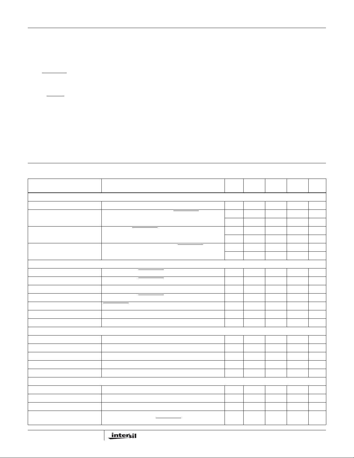
TABLE 1. SUMMARY OF FEATURES
ENHANCED
PART
NUMBER
NO. OF
Tx.
NO. OF
Rx. CONFIG. QFN PKG.
MONITOR Rx.
(R
OUTB
ISL4238E 5 3 DCE 5x5 1 250 NO YES YES
ISL4244E 3 5 DTE 5x5 1 250 NO YES YES
ISL4245E 3 5 DTE 5x5 1 1000 NO YES YES
NO. OF
DATA
RATE
)
(kbps)
Rx. ENABLE
FUNCTION?
MANUAL
POWER-
DOWN?
AUTOMATIC
POWERDOWN
FUNCTION?
Ordering Information
PART NO.
(BRAND)
ISL4238EIR
(4238EIR)
ISL4238EIRZ
(4238EIR) (Note)
ISL4238EIR-T
(4238EIR)
ISL4238EIRZ-T
(4238EIR) (Note)
ISL4244EIR
(4244EIR)
ISL4244EIRZ
(4244EIR) (Note)
ISL4244EIR-T
(4244EIR)
ISL4244EIRZ-T
(4244EIR) (Note)
TEMP.
RANGE (°C) PACKAGE
-40 to 85 32 Ld QFN L32.5x5
-40 to 85 32 Ld QFN (Pb-free) L32.5x5
-40 to 85 Tape & Reel L32.5x5
-40 to 85 Tape & Reel (Pb-free) L32.5x5
-40 to 85 32 Ld QFN L32.5x5
-40 to 85 32 Ld QFN (Pb-free) L32.5x5
-40 to 85 Tape & Reel L32.5x5
-40 to 85 Tape & Reel (Pb-free) L32.5x5
Pinouts
ISL4238E (QFN)
TOP VIEW
PKG.
DWG. #
Ordering Information (Continued)
PART NO.
(BRAND)
ISL4245EIR
(4245EIR)
ISL4245EIRZ
(4245EIR) (Note)
ISL4245EIR-T
(4245EIR)
ISL4245EIRZ-T
(4245EIR) (Note)
NOTE: Intersil Pb-free products employ special Pb-free material
sets; molding compounds/die attach materials and 100% matte tin
plate termination finish, which is compatible with both SnPb and
Pb-free soldering operations. Intersil Pb-free products are MSL
classified at Pb-free peak reflow temperatures that meet or exceed
the Pb-free requirements of IPC/JEDEC J Std-020B.
TEMP.
RANGE (°C) PACKAGE
-40 to 85 32 Ld QFN L32.5x5
-40 to 85 32 Ld QFN (Pb-free) L32.5x5
-40 to 85 Tape & Reel L32.5x5
-40 to 85 Tape & Reel (Pb-free) L32.5x5
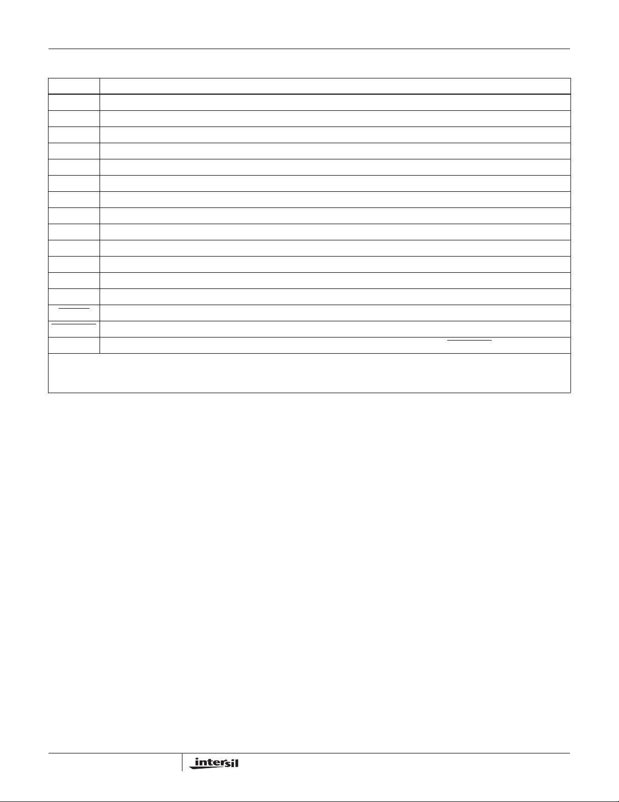
ISL4244E, ISL4245E (QFN)
TOP VIEW
PKG.
DWG. #
T1
T2
T3
T4
T5
OUT
OUT
OUT
R1
R2
OUT
R3
OUT
R1
V+
OUTB
V
T5
CC
IN
NC
NC
NC
V-
C2-
C2+
C1+
32 31 30 29 28 27 26 25
C1-
24
T1
IN
23
T2
22
IN
T3
IN
21
R1
20
OUT
R2
19
OUT
T4
18
IN
R3
17
OUT
T1
T2
T3
R1
R2
R3
R4
R5
OUT
OUT
OUT
1
IN
2
IN
3
IN
4
IN
5
IN
6
7
8
9 10111213141516
NC
T3INT2INT1
IN
OUT
R5
C2-
GND
C2+
V-
32 31 30 29 28 27 26 25
1
2
3
4
IN
5
IN
6
7
IN
8
9 10111213141516
NC
FORCEON
FORCEOFF
C1+
NC
INVALID
V+
R4
CC
NC
V
GND
24
C1-
23
FORCEON
22
FORCEOFF
21
INVALID
20
R2
OUTB
19
R1
18
OUT
R2
17
OUT
NC
OUT
OUT
R3
2
ISL4238E, ISL4244E, ISL4245E
www.BDTIC.com/Intersil
Pin Descriptions
PIN FUNCTION
V
CC
V+ Internally generated positive transmitter supply (+5.5V).
V- Internally generated negative transmitter supply (-5.5V).
GND Ground connection.
C1+ External capacitor (voltage doubler) is connected to this lead.
C1- External capacitor (voltage doubler) is connected to this lead.
C2+ External capacitor (voltage inverter) is connected to this lead.
C2- External capacitor (voltage inverter) is connected to this lead.
T
T
OUT
R
R
OUT
R
OUTB
INVALID
FORCEOFF Active low to shut down transmitters and on-chip power supply. This overrides any automatic circuitry and FORCEON (see T ab le 2).
FORCEON Active high input to override automatic powerdown circuitry thereby keeping transmitters active. (FORCEOFF
NOTE:
1. ISL4238E input pins incorporate positive feedback resistors. Once the input is driven to a valid logic level, the feedback resistor maintains that
logic level until V
System power supply input (2.7V to 5.5V).
TTL/CMOS compatible transm it ter I nput s. (Note 1)
IN
±15kV ESD Protected, RS-232 level (nominally ±5.5V) transmitter outputs.
±15kV ESD Protected, RS-232 compatible receiver in puts.
IN
TTL/CMOS level receiver outputs.
TTL/CMOS level, noninverting, always enabled receiver outputs.
Active low output that indicates if no valid RS-232 levels are present on any receiver input.
is removed. Unused transmitter inputs may be left unconnected by the user.
CC
must be high).
3
Typical Operating Circuits
www.BDTIC.com/Intersil
TTL/CMOS
ISL4238E, ISL4244E, ISL4245E
ISL4238E
+3.3V
NOTE 2
LOGIC
LEVELS
0.1µF
0.1µF
R1
+
0.1µF
28
C
1
C
2
T1
T2
T3
T4
T5
OUTB
IN
IN
IN
IN
IN
C1+
V
+
24
29
+
31
23
22
21 3
18 6
15 8
14
CC
C1C2+
C2-
26
T
1
T
2
T
3
T
4
T
5
V+
27
C
3
+
0.1µF
C
0.1µF
+
OUT
OUT
OUT
OUT
OUT
NOTE 2
4
RS-232
LEVELS
32
V-
1
T1
2
T2
T3
T4
T5
NOTE:
2. For V
5kΩ
5kΩ
5kΩ
4
R1
IN
519
R2
IN
RS-232
LEVELS
717
R3
IN
R1
R2
R3
TO POWER
CONTROL
LOGIC
= 3.15V (3.3V -5%), use C1 - C4 = 0.1µF or greater. For VCC = 3.0V (3.3V -10%), use C1 - C4 = 0.22µF or greater.
CC
20
OUT
OUT
OUT
10
11
V
CC
12
R
1
R
2
R
3
FORCEON
FORCEOFF
INVALID
GND
30
4
ISL4238E, ISL4244E, ISL4245E
www.BDTIC.com/Intersil
Typical Operating Circuits (Continued)
+3.3V
C
1
0.1µF
C
2
0.1µF
T1
IN
T2
IN
T3
IN
ISL4244E, ISL4245E
+
0.1µF
28
C1+
+
23
C1-
29
C2+
+
30
C2-
12
11
10 8
26
V
CC
T
T
T
V+
V-
1
2
3
27
C
3
+
0.1µF
31
C
4
0.1µF
+
6
T1
OUT
7
T2
T3
OUT
OUT
RS-232
LEVELS
TTL/CMOS
LOGIC LEVELS
CONTROL LOGIC
R2
OUTB
R1
OUT
R2
OUT
R3
OUT
R4
OUT
R5
OUT
V
CC
TO POWER
19
18
22
FORCEON
21
FORCEOFF
20
INVALID
R
R
R
R
R
1
2
3
4
5
GND
1
R1
IN
5kΩ
217
R2
IN
5kΩ
315
R3
5kΩ
414
R4
5kΩ
513
5kΩ
24
R5
RS-232
IN
LEVELS
IN
IN
5
ISL4238E, ISL4244E, ISL4245E
www.BDTIC.com/Intersil
Absolute Maximum Ratings Thermal Information
VCC to Ground. . . . . . . . . . . . . . . . . . . . . . . . . . . . . . . . -0.3V to 6V
V+ to Ground . . . . . . . . . . . . . . . . . . . . . . . . . . . . . . . . . -0.3V to 7V
V- to Ground. . . . . . . . . . . . . . . . . . . . . . . . . . . . . . . . . +0.3V to -7V
V+ to V- . . . . . . . . . . . . . . . . . . . . . . . . . . . . . . . . . . . . . . . . . . . 14V
Input Voltages
, FORCEOFF, FORCEON. . . . . . . . . . . . . . . . . . . -0.3V to 6V
T
IN
. . . . . . . . . . . . . . . . . . . . . . . . . . . . . . . . . . . . . . . . . . . . ±25V
R
IN
Output Voltages
. . . . . . . . . . . . . . . . . . . . . . . . . . . . . . . . . . . . . . . . . ±13.2V
T
OUT
, INVALID. . . . . . . . . . . . . . . . . . . . . . . . -0.3V to VCC +0.3V
R
OUT
Short Circuit Duration
. . . . . . . . . . . . . . . . . . . . . . . . . . . . . . . . . . . . . Continuous
T
OUT
ESD Rating . . . . . . . . . . . . . . . . . . . . . . . . . See Specification Table
CAUTION: Stresses above those listed in “Absolute Maximum Ratings” may cause permanent damage to the device. This is a stress only rating and operation of the
device at these or any other conditions above those indicated in the operational sections of this specification is not implied.
NOTE:
is measured in free air with the component mounted on a high effective thermal conductivity test board with “direct attach” features. See
3. θ
JA
Tech Brief TB379, and Tech Brief TB389.
Thermal Resistance (Typical, Note 3)
32 Ld QFN Package. . . . . . . . . . . . . . . . . . . . . . . . . 32
Moisture Sensitivity (see Technical Brief TB363)
QFN Package. . . . . . . . . . . . . . . . . . . . . . . . . . . . . . . . . . . Level 1
Maximum Junction Temperature (Plastic Package) . . . . . . . 150
Maximum Storage Temperature Range. . . . . . . . . . -65
Maximum Lead Temperature (Soldering 10s) . . . . . . . . . . . . 300
θ
(oC/W)
JA
o
C to 150oC
Operating Conditions
Temperature Range
ISL42XXEIR. . . . . . . . . . . . . . . . . . . . . . . . . . . . . . -40
o
C to 85oC
o
o
C
C
Electrical Specifications Test Conditions: ISL4238E V
ISL424XE V
PARAMETER TEST CONDITIONS
DC CHARACTERISTICS
Operating Voltage Range Full 2.7 - 5.5 V
Supply Current, Automatic
Powerdown
Supply Current, Powerdown All R
Supply Current,
Automatic Powerdown Disabled
LOGIC AND TRANSMITTER INPUTS AND RECEIVER OUTPUTS
Input Logic Threshold Low T
Input Logic Threshold High T
Transmitter Input Hysteresis 25 - 0.5 - V
Input Leakage Current T
Output Leakage Current FORCEOFF
Output Voltage Low I
Output Voltage High I
RECEIVER INPUTS
Input Voltage Range Full -25 - 25 V
Input Threshold Low V
Input Threshold High V
Input Hysteresis 25 - 0.5 - V
Input Resistance Full 3 5 7 kΩ
TRANSMITTER OUTPUTS
Output Voltage Swing All Transmitter Outputs Loaded with 3kΩ to Ground Full ±5.0 ±5.4 - V
Output Resistance V
Output Short-Circuit Current Full - ±35 ±60 mA
Output Leakage Current V
All R
IN
IN
All Outputs Unloaded, FORCEON = FORCEOFF
= 3.0V
V
CC
, FORCEON, FORCEOFF Full - - 0.8 V
IN
, FORCEON, FORCEOFF, VCC = 3.6V Full 2.0 - - V
IN
, FORCEON, FORCEOFF (ISL4238E, Note 4) Full - ±0.01 ±1.0 µA
IN
= 1.6mA Full - - 0.4 V
OUT
= -1.0mA Full V
OUT
= 3.0V Full - 1.0 0.6 V
CC
= 3.6V Full 2.4 1.5 - V
CC
= V+ = V- = 0V, Transmitter Output = ±2V Full 300 10M - Ω
CC
OUT
Automatic Powerdown or FORCEOFF
= 3V to 5.5V, C1 - C4 = 0.1µF; Unless Otherwise Specified. Typicals are at TA = 25oC
CC
Open, FORCEON = GND, FORCEOFF = V
Open, FORCEOFF = GND 25 - 3 300 nA
= GND Full - ±0.05 ±10 µA
= ±12V, VCC = 0V or 3V to 5.5V,
= 3.15V to 5.5V, C1 - C4 = 0.1µF; VCC = 3V, C1 - C4 = 0.22µF;
CC
TEMP
o
(
C) MIN TYP MAX UNITS
CC
= VCC,
= GND
25 - 3 300 nA
Full 50 300 nA
Full 50 300 nA
25 - 0.3 1.0 mA
Full 0.3 1.5 mA
-0.6 V
CC
Full - - ±25 µA
-0.1 - V
CC
6

ISL4238E, ISL4244E, ISL4245E
www.BDTIC.com/Intersil
Electrical Specifications Test Conditions: ISL4238E V
ISL424XE V
PARAMETER TEST CONDITIONS
ENHANCED AUTOMATIC POWERDOWN (FORCEON = GND, FORCEOFF = VCC)
Receiver Input Thresholds to
INVALID
Receiver Input Thresholds to
INVALID
INVALID
INVALID
Receiver Positive or Negative
Threshold to INVALID
(t
Receiver Positive or Negative
Threshold to INVALID
(t
Receiver Positive or Negative
Threshold to INVALID
(t
Receiver or Transmitter Edge to
Transmitters Enabled Delay (t
Receiver or Transmitter Edge to
Transmitters Disabled Delay
(t
TIMING CHARACTERISTICS
Maximum Data Rate
ISL4238E/44E
Maximum Data Rate
ISL4245E
Receiver Propagation Delay Receiver Input to Receiver
Receiver Skew t
Transmitter Propagation Delay
ISL4238E/44E
Transmitter Skew ISL4238E/44E t
Transmitter Propagation Delay
ISL4245E
Transmitter Skew ISL4245E t
High
Low
, Output Voltage Low I
, Output Voltage High I
)
INVH
)
INVL
)
INVL
AUTOPWDN
)
High Delay
Low Delay
Low Delay
See Fi g u r e 6 Full -2.7 - 2.7 V
See Figure 6 Full -0.3 - 0.3 V
= 1.6mA Full - - 0.4 V
OUT
= -1.0mA Full VCC-0.6 - - V
OUT
ISL4238E 25 - 60 100 µs
ISL4244E/45E 25 - 30 50 µs
Note 5 Full - 20 100 µs
)
WU
Note 5 Full 15 30 60 sec
R
=3kΩ, CL= 1000pF, One Transmitter Switching Full 250 500 - kbps
L
= 3kΩ, One Transmitter
R
L
Switching
Output,
= 150pF
C
L
- t
PHL
Transmitter Input to
Transmitter Output,
C
= 1000pF, RL = 3kΩ
L
- t
PHL
Transmitter Input to
Transmitter Output,
C
= 1000pF, RL = 3kΩ
L
- t
PHL
= 3V to 5.5V, C1 - C4 = 0.1µF; Unless Otherwise Specified. Typicals are at TA = 25oC
CC
, CL = 150pF 25 - 120 250 ns
PLH
(Note 7), RL = 3kΩ, CL = 1000pF 25 - 50 200 ns
PLH
(Note 6), RL = 3kΩ, CL = 1000pF 25 - 50 200 ns
PLH
= 3.15V to 5.5V, C1 - C4 = 0.1µF; VCC = 3V, C1 - C4 = 0.22µF;
CC
CL = 1000pF Full 250 900 - kbps
V
= 3V to 4.5V, CL = 250pF Full 1000 2000 - kbps
CC
= 4.5V to 5.5V,
V
CC
C
= 1000pF
L
t
PHL
t
PLH
t
PHL
t
PLH
t
PHL
t
PLH
TEMP
o
C) MIN TYP MAX UNITS
(
25 - 0.5 1 µs
Full - 0.9 1.5 µs
Full 100 150 µs
Full 40 60 µs
Full 1000 1500 - kbps
25 - 0.15 0.3 µs
Full - 0.2 0.35 µs
25 - 0.3 0.5 µs
Full - 0.35 0.55 µs
Full - 150 300 ns
25 - 0.75 1 µs
Full - 0.85 1.1 µs
25 - 0.8 1 µs
Full - 0.9 1.1 µs
Full - 100 250 ns
25 - 0.4 0.8 µs
Full - 0.5 0.8 µs
25 - 0.35 0.7 µs
Full - 0.4 0.7 µs
Full - 60 250 ns
7

ISL4238E, ISL4244E, ISL4245E
www.BDTIC.com/Intersil
Electrical Specifications Test Conditions: ISL4238E V
ISL424XE V
PARAMETER TEST CONDITIONS
Receiver Output Enable Time Normal Operation, RL = 1kΩ to 0.5VCC, CL = 15pF 25 - 200 350 ns
Receiver Output Disable Time Normal Operation, R
Transmitter Output Enable Time
ISL4238E/44E/45E
Transmitter Output Disable Time
ISL4238E/44E/45E
Transition Region Slew Rate
ISL4238E/44E
Transition Region Slew Rate
ISL4245E
ESD PERFORMANCE
RS-232 Pins (T
All Other Pins Human Body Model 25 - ±3-kV
NOTES:
4. ISL4238E inputs utilize a positive feedback resistor. The input current is negligible when the input is at either supply rail.
5. An “edge” is defined as a transition through the transmitter or receiver input thresholds.
6. Skew is measured at the receiver input switching points (1.4V).
7. Skew is measured at the transmitter zero crossing points.
, RIN) Human Body Model 25 - ±15 - kV
OUT
Normal Operation, R
Normal Operation, R
V
= 3V to 3.6V,
CC
=3kΩ to 7kΩ,
R
L
Measured From 3V to -3V
or -3V to 3V
V
= 3V to 3.6V, RL = 3kΩ to 7kΩ, Measured From 3V to
CC
-3V or -3V to 3V, C
IEC6100-4-2 Air Gap Discharge 25 - ±15 - kV
IEC6100-4-2 Contact Discharge 25 - ±8-kV
= 3V to 5.5V, C1 - C4 = 0.1µF; Unless Otherwise Specified. Typicals are at TA = 25oC
CC
L
L
L
= 150pF to 1000pF
L
= 3.15V to 5.5V, C1 - C4 = 0.1µF; VCC = 3V, C1 - C4 = 0.22µF;
CC
TEMP
o
C) MIN TYP MAX UNITS
(
Full - 200 400 ns
= 1kΩ to 0.5VCC, CL = 15pF 25 - 350 500 ns
Full - 400 600 ns
= 3kΩ, CL = 1000pF 25 - 25 40 µs
Full - 35 50 µs
= 3kΩ, CL = 1000pF 25 - 2.5 4 µs
Full - 2.7 4 µs
= 150pF to 1000pF 25 6 11 30 V/µs
C
L
Full 6 10 30 V/µs
C
= 150pF to 2500pF 25 4 9 30 V/µs
L
Full 4 8 30 V/µs
25 24 40 150 V/µs
Full 24 35 150 V/µs
Detailed Description
These interface ICs operate from a single +2.7V to +5.5V
supply, guarantee a 250kb ps (ISL4238E/44E) / 1Mbps
(ISL4245E) minimum data rate, require only four small
external 0.1µF capacitors, feature low pow er co nsu mp ti o n ,
and meet all ElA RS-232C and V.28 specifications. The
circuit is divided into three sections: The charge pump, the
transmitters, and the receivers.
Charge-Pump
Intersil’s new RS-232 family utilizes regulated on-chip dual
charge pumps as voltage doublers, and voltage inverters to
generate ±5.5V transmitter supplies from a V
low as 3.0V. This allows these devices to maintain RS-232
compliant output levels over the ±10% tolerance range of
3.3V powered systems. The efficient on-chip power supplies
require only four small, external 0.1µF capacitors for the
voltage doubler and inverter functions. The charge pumps
operate discontinuously (i.e., they turn off as soon as the V+
and V- supplies are pumped up to the nominal values),
resulting in significant power savings.
8
supply as
CC
Transmitters
The transmitters are proprietary, low dropout, inverting
drivers that translate TTL/CMOS inputs to EIA/TIA-232
output levels. Coupled with the on-chip ±5.5V supplies, thes e
transmitters deliver true RS-232 levels over a wide range of
single supply system voltages.
Transmitter outputs disable and assume a high impedance
state when the device enters the powerdown mode (see
Table 2). These outputs may be driven to ±12V when
disabled.
The ISL4238E/44E guarantee a 250kbps data rate for full
load conditions (3kΩ and 1000pF), V
transmitter operating at full speed. Under more typical
conditions of V
≥ 3.3V, RL = 3kΩ, and CL = 250pF, one
CC
transmitter easily operates at 1Mbps.
The ISL4245E guarantees a 1Mbps data rate for full load
conditions (3kΩ and 250pF), V
CC
transmitter operating at full speed. Under more typical
conditions of V
≥ 3.3V, RL= 3kΩ, and CL = 250pF, one
CC
transmitter easily operates at 1.4Mbps.
≥ 3.0V, with one
CC
≥ 3.0V, with one

ISL4238E, ISL4244E, ISL4245E
www.BDTIC.com/Intersil
TABLE 2. POWERDOWN LOGIC TRUTH TABLE
RS-232
RCVR OR
XMTR
EDGE
WITHIN 30
SEC?
NO H H Active Active Active NO L Normal Operation (Enhanced
NO H H Active Active Active YES H
YES H L Active Active Active NO L Normal Operation (Enhanced
YES H L Active Active Active YES H
NO H L High-Z Active Active NO L Powerdown Due to Enhanced
NO H L High-Z Active Active YES H
X L X High-Z High-Z Active NO L Manual Powerdown
X L X High-Z High-Z Active YES H
INVALID
X NOTE 8 NOTE 8 Active Active Active YES H Normal Operation
X NOTE 8 NOTE 8 High-Z High-Z Active NO L Forced Auto Powerdown
NOTE:
8. Input is connected to INVALID
FORCEOFF
INPUT
DRIVING FORCEON AND FORCEOFF (EMULATES AUTOMATIC POWERDOWN)
FORCEON
INPUT
Output.
TRANSMITTER
OUTPUTS
RECEIVER
OUTPUTS
R
OUTB
OUTPUTS
LEVEL
PRESENT
AT
RECEIVER
INPUT?
INVALID
OUTPUT MODE OF OPERATION
Auto Powerdown Disabled)
Auto Powerdown Enabled)
Auto Powerdown Logic
Transmitter inputs on the ISL424XE float if left unconnected,
and may cause I
increases. Connect unused inputs to
CC
GND for the best performance. ISL4238E transmitter inputs
incorporate an active positive feedback resistor that
maintains the last input state in the absence of a forcing
signal, so unused transmitter inputs may be left
unconnected.
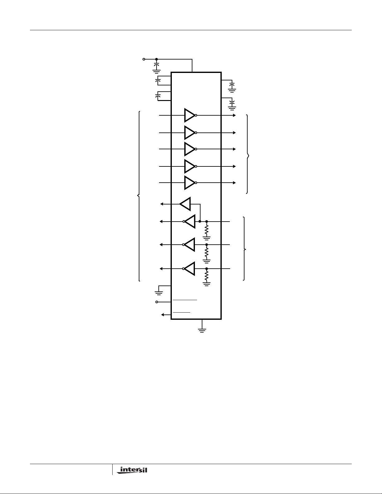
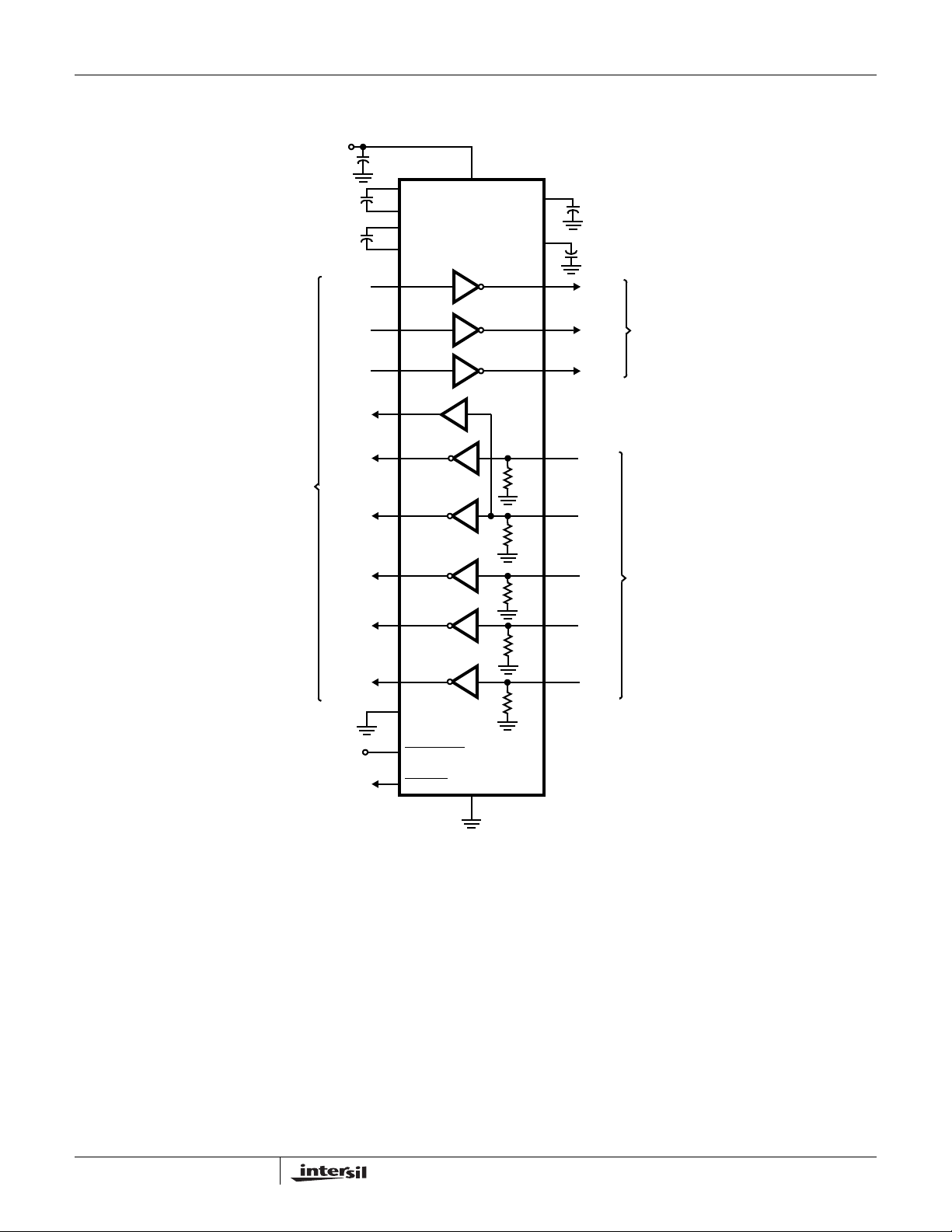
Receivers
ISL4238E/4XE devices contain standard inverting receivers
which can tristate via the FORCEOFF
Additionally, they include a noninverting (monitor) receiver
(denoted by the R
label) that is always active,
OUTB
regardless of the state of any control lines. Both receiver
types convert RS-232 signals to CMOS output levels and
accept inputs up to ±25V while presenting the required 3kΩ
to 7kΩ input impedance (see Figure 1) even if the power is
off (V
= 0V). The receivers’ Schmitt trigger input stage
CC
uses hysteresis to increase noise immunity and decrease
errors due to slow input signal transitions.
V
CC
R
XIN
-25V ≤ V
FIGURE 1. INVERTING RECEIVER CONNECTIONS
RIN
≤ +25V
GND
5kΩ
The ISL4238E/4XE inverting receivers disable during forced
(manual) powerdown, but not during automatic powerdown
(see Table 2). Conversely, the monitor receiver remains
active even during manual powerdown making it extremely
useful for Ring Indicator monitoring. Standard receivers
driving powered down peripherals must be disabled to
control line.
R
XOUT
GND ≤ V
ROUT
≤ V
CC
prevent current flow through the peripheral’s protection
diodes (see Figures 2 and 3). This renders them useless for
wake up functions, but the corresponding monitor receiver
can be dedicated to this task as shown in Figure 3.
V
CC
V
CC
V
OUT = VCC
Rx
POWERED
DOWN
UART
Tx
= GND
GND
FIGURE 2. POWER DRAIN THROUGH POWERED DO WN
PERIPHERAL
SHDN
V
CC
CURRENT
FLOW
OLD
RS-232 CHIP
Low Power Operation
These 3V devices require a nominal supply current of
0.3mA, even at V
powerdown mode). This is considerably less than the 5mA to
11mA current required by comparable 5V RS-232 devices,
allowing users to reduce system power simply by switching
to this new family.
= 5.5V, during normal operation (not in
CC
9

ISL4238E, ISL4244E, ISL4245E
www.BDTIC.com/Intersil
V
CC
TRANSITION
DETECTOR
TO
WAKE-UP
LOGIC
V
CC
R
X
POWERED
DOWN
UART
FIGURE 3. DISABLED RECEIVERS PREVENT POWER DRAIN
T
X
FORCEOFF = GND
V
OUT =
R
OUTB
R
HI-Z
OUT
T1
IN
ISL4238E/4XE
R
T1
IN
OUT
Po werdown Functionality
The already low current requirement drops significantly
when the device ente rs powerdown mode. In powerdown ,
supply current drops to 10nA, because the on-chip charge
pump turns off (V+ collapses to V
and the transmitter outputs tristate. Inverting receiver
outputs disable only in manual powerdown; refer to Table 2
for details. This micro-power mode makes these devices
ideal for battery powered and portable applications.
Software Controlled (Manual) Powerdown
These devices allow the user to force the IC into the low
power, standby state, and utilize a two pin approach where
the FORCEON and FORCEOFF
mode. For always enabled operation, FORCEON and
FORCEOFF
active and powerdown modes, under logic or software
control, only the FORCEOFF
FORCEON state isn’t critical, as FORCEOFF
over FORCEON. Ne vertheless, if strictly manual control over
powerdown is desired, the user must strap FORCEON high
to disable the enhanced automatic powerdown circuitry.
ISL4238E/4XE inverting (standard) receiver outputs also
disable when the device is in manual powerdown, thereby
eliminating the possible current path through a shutdown
peripheral’s input protection diode (see Figures 2 and 3).
Connecting FORCEOFF
the enhanced automatic powerdown feature, enabling them
to function as a manual SHUT DOWN
With any of the above control schemes, the time required to
exit powerdown, and resume transmission is only 100µs.
are both strapped high. To switch between
and FORCEON together disables
, V- collapses to GND),
CC
inputs determine the IC’s
input need be driven. The
dominates
input (see Figure 4).
FORCEOFF
PWR
MGT
LOGIC
CPU
FIGURE 4. CONNECTIONS FOR MANUAL POWERDOWN
WHEN NO VALID RECEIVER SIGNALS ARE
PRESENT
I/O
UART
FORCEON
INVALID
ISL4238E/4XE
When using both manual and enhanced automatic
powerdown (FORCEON = 0), the ISL4238E/4XE won’t
power up from manual powerdown until both FORCEOFF
and FORCEON are driven high, or until a transition occurs
on a receiver or transmitter input. Figure 5 illustrates a circuit
for ensuring that the ISL4238E/4XE powers up as soon as
FORCEOFF
switches high. The rising edge of the Master
Powerdown signal forces the device to power up, and the
ISL4238E/4XE returns to enhanced automatic powerdown
mode an RC time constant after this rising edge. The time
constant isn’t critical, because the ISL4238E/4XE remains
powered up for 30 seconds after the FORCEON falling edge,
even if there are no signal transitions. This gives slow-towake systems (e.g., a mouse) plenty of time to start
transmitting, and as long as it starts transmitting within 30
seconds both systems remain enabled.
POWER
MANAGEMENT
UNIT
FIGURE 5. CIRCUIT TO ENSURE IMMEDIATE PO WER UP
WHEN EXITING FORCED POWERDOWN
MASTER POWERDOWN LINE
0.1µF
FORCEOFF FORCEON
ISL4238E/4XE
1MΩ
INVALID Output
The INVALID output always indicates (see Table 2) whether
or not 30µs have elapsed with invalid RS-232 signals (see
Figures 6 and 9) persisting on all of the receiver inputs,
giving the user an easy way to determine when the interface
block should power down. Invalid receiver levels occur
whenever the driving peripheral’s outputs are shut off
(powered down) or when the RS-232 interface cable is
disconnected. In the case of a disconnected interface cable
where all the receiver inputs are floating (but pulled to GND
10

ISL4238E, ISL4244E, ISL4245E
www.BDTIC.com/Intersil
by the internal receiver pull down resistors), the INVALID
logic detects the invalid levels and drives the output low . The
power management logic then uses this indicator to power
down the interface block. Reconnecting the cable restores
valid levels at the receiver inputs, INVALID
switches high,
and the power management logic wakes up the interface
block. INVALID
can also be used to indicate the DTR or
RING INDICATOR signal, as long as the other receiver
inputs are floating, or driven to GND (as in the case of a
powered down driver).
INVALID
level on a receiver input. INVALID
switches high 1µs after detecting a valid RS-232
operates in all modes
(forced or automatic powerdown, or forced on), so it is also
useful for systems employing manual powerdown circuitry.
2.7V
0.3V
-0.3V
-2.7V
FIGURE 6. DEFINITION OF VALID RS-232 RECEIVER LEVELS
VALID RS-232 LEVEL - INVALID
INDETERMINATE
INVALID LEVEL - INVALID
INDETERMINATE
VALID RS-232 LEVEL - INVALID
= 0
= 1
= 1
Enhanced Automatic Powerdown
Even greater power savings is availab le by using these devices
which feature an enhanced automatic powerdown function.
When the enhanced powerdown logic determines that no
transitions have occurred on any of the transmitter nor receiv er
inputs for 30 seconds, the charge pump and transmitters
powerdown, thereby reducing supply current to
ISL4238E/4XE automatically powers back up whenever it
detects a transition on one of these inputs. This automatic
powerdown feature provides additional system pow er sa vings
without changes to the existing operating system.
10nA. The
FORCEOFF
T_IN
R_IN
FIGURE 7. ENHANCED AUTOMATIC POWERDOWN LOGIC
EDGE
DETECT
EDGE
DETECT
FORCEON
S
30sec
TIMER
R
AUTOPWDN
on the state of the ISL4238E/4XE (see the next sections for
methods of utilizing INVALID
to power down the device).
The time to recover from automatic powerdown mode is
typically 100µs.
Emulating Standard Automatic Powerdown
If enhanced automatic powerdown isn’t desired, the user can
implement the standard automatic powerdown feature (mimics
the function on the ISL4243E) by connecting the INV ALID
output to the FORCEON and FORCEOFF
inputs, as shown in
Figure 8. After 30µs of invalid receiver levels, INVALID
low and drives the ISL4238E/4XE into a forced powerdo wn
condition. INVALID
switches high as soon as a receiver input
senses a valid RS-232 level, forcing the ISL4238E/4XE to
power on. See the “INVALID
FORCEOFF
” section of Table 2 for an operational summary.
DRIVING FORCEON AND
This operational mode is perfect for handheld devices that
communicate with another computer via a detachable cable.
Detaching the cable allows the internal receiver pull-down
resistors to pull the inputs to GND (an invalid RS-232 lev el),
causing the 30µs timer to time-out and drive the IC into
powerdown. Reconnecting the cable
restores valid lev els ,
causing the IC to power back up.
FORCEON
INVALID
ISL4238E/4XE
FORCEOFF
switches
Enhanced automatic powerdown operates when the
FORCEON input is low, and the FORCEOFF
input is high.
Tying FORCEON high disables automatic powerdown, but
manual powerdown is always available via the overriding
FORCEOFF
input. Table 2 summarizes the enhanced
CPU
automatic powerdown functionality.
Figure 7 illustrates the enhanced powerdown control logic.
Note that once the ISL4238E/4XE enters powerdown
FIGURE 8. CONNECTIONS FOR AUTOMA TIC PO WERDOWN
(manually or automatically), the 30 second timer remains
timed out (set), keeping the ISL4238E/4XE powered down
until FORCEON transitions high, or until a transition occurs
on a receiver or transmitter input.
The INVALID
output signal switches low to indicate that
invalid levels have persisted on all of the receiver inputs for
more than 30µs (see Figure 9), but this has no direct effect
Hybrid Automatic Powerdown Options
For devices which communicate only through a detachable
cable, connecting INVALID
FORCEON = 0) may be a desirable configuration. While the
11
I/O
UART
WHEN NO VALID RECEIVER SIGNALS ARE
PRESENT
to FORCEOFF (with

ISL4238E, ISL4244E, ISL4245E
www.BDTIC.com/Intersil
RECEIVER
INPUTS
TRANSMITTER
INPUTS
TRANSMITTER
OUTPUTS
INVALID
OUTPUT
OUTPUT
V+
V
CC
t
INVL
0
V-
FIGURE 9. ENHANCED AUTOMATIC POWERDOWN AND INVALID TIMING DIAGRAMS
t
INVH
t
AUTOPWDN
cable is attached INVALID and FORCEOFF remain high, so
the enhanced automatic powerdown logic powers down the
RS-232 device whenever there is 30 seconds of inactivity on
the receiver and transmitter inputs. Detaching the cable
allows the receiver inputs to drop to an invalid level (GND),
so INVALID
switches low and forces the RS-232 device to
power down. The ISL4238E/4XE remains powered down
until the cable is reconnected (INVALID
= FORCEOFF = 1)
and a transition occurs on a receiver or transmitter input (see
Figure 7). For immediate power up when the cable is
reattached, connect FORCEON to FORCEOFF
through a
network similar to that shown in Figure 5.
Capacitor Selection
The ISL4238E charge pumps require 0.1µF, or greater,
capacitors for 3.3V (5% tolerance) operation. For other
supply voltages refer to Table 3 for capacitor value s. Do not
use values smaller than those listed in Table 3.
TABLE 3. REQUIRED CAPACITOR VALUES (ISL4238E)
V
(V) C1 (µF) C2, C3, C4 (µF)
CC
3.0 to 3.6 (3.3V ±10%) 0.22 0.22
3.15 to 3.6 (3.3V ±5%) 0.1 0.1
4.5 to 5.5 0.047 0.33
3.0 to 5.5 0.22 1
The ISL4244E/45E charge pumps require 0.1µF capacitors
for proper operation. Increasing the capacitor values (by a
factor of 2) reduces ripple on the transmitter outputs and
slightly reduces power consumption. C
increased without increasing C
increase C
without also increasing C2, C3, and C4 to
1
maintain the proper ratios (C
’s value, however, do not
1
to the other capacitors).
1
, C3, and C4 can be
2
INVALID
}
REGION
t
t
WU
AUTOPWDN
t
WU
When using minimum required capacitor values, make sure
that capacitor values do not degrade excessively with
temperature. If in doubt, use capacitors with a larger nominal
value. The capacitor’s equivalent series resistance (ESR)
usually rises at low temperatures and it influences the
amount of ripple on V+ and V-.
Po wer Supply Decoupling
In most circumstances a 0.1µF bypass capacitor is
adequate. In applications that are particularly sensitive to
power supply noise, decouple V
capacitor of the same value as the charge-pump capacitor C
to ground with a
CC
1
Connect the bypass capacitor as close as possible to the IC.
Transmitter Outputs when Exiting
Powerdown
Figure 10 shows the response of two transmitter outputs
when exiting powerdown mode. As they activate, the two
transmitter outputs properly go to opposite RS-232 levels,
with no glitching, ringing, nor undesirable transients. Each
transmitter is loaded with 3kΩ in parallel with 2500pF. Note
that the transmitters enable only when the magnitude of the
supplies exceed approximately 3V.
Operation Down to 2.7V
ISL4238E/4XE transmitter outputs meet RS-562 levels
(
±3.7V), at the full data rate, with V
RS-562 levels typically ensure interoperability with RS-232
devices.
as low as 2.7V.
CC
.
12

5V/DIV
www.BDTIC.com/Intersil
FORCEOFF
ISL4238E, ISL4244E, ISL4245E
for a single transmitter driving 250pF and an RS-232 load at
1Mbps. The static transmitters were also loaded with an
T1
RS-232 receiver.
V
CC
0.1µF
+
2V/DIV
T2
VCC = +3.3V
C1 - C4 = 0.1µF
TIME (20µs/DIV.)
FIGURE 10. TRANSMITTER OUTPUTS WHEN EXITING
POWERDOWN
Mouse Driveability
The ISL424XE are specifically designed to power a serial
mouse while operating from low voltage supplies. Figure 11
shows the transmitter output voltages under increasing load
current. The on-chip switching regulator ensures the
transmitters will supply at least
±5V during worst case
conditions (15mA for paralleled V+ transmitters, 7.3mA for
single V - tr ansmit ter).
6
5
V
4
3
2
1
0
-1
-2
V
CC
-3
-4
-5
TRANSMITTER OUTPUT VOLTAGE (V)
-6
0246810
= 3.0V
V
CC
T1
V
+
OUT
T2
ISL424XE
-
T3
13579
LOAD CURRENT PER TRANSMITTER (mA)
V
OUT
FIGURE 11. TRANSMITTER OUTPUT VOLTAGE vs LOAD
CURRENT (PER TRANSMITTER, i.e., DOUBLE
CURRENT AXIS FOR TOTAL V
OUT+
+
OUT
V
-
OUT
CURRENT)
High Data Rates
The ISL4238E/4XE maintain the RS-232 ±5V minimum
transmitter output voltages even at high data rates. Figure 12
details a transmitter loopback test circuit, and Figure 13
illustrates the ISL4238E/44E loopback test result at
120kbps. For this test, all transmitters were simultaneously
driving RS-232 loads in parallel with 1000pF, at 120kbps.
Figure 14 shows the ISL4238E/44E loopback results for a
single transmitter driving 1000pF and an RS-232 load at
250kbps. Figure 15 illustrates the ISL4245E loopback test
result at 250kbps. For this test, all transmitters were
simultaneously driving RS-232 loads in parallel with 1000pF,
at 250kbps. Figure 16 shows the ISL4245E loopback results
V
+
C
1
+
C
2
V
CC
C1+
C1-
C2+
C2-
T
IN
R
OUT
FORCEON
FORCEOFF
CC
ISL4238E/4XE
T
OUT
V+
V-
R
IN
5k
+
+
FIGURE 12. TRANSMITTER LOOPBACK TEST CIRCUIT
5V/DIV.
T1
IN
T1
OUT
R1
OUT
VCC = +3.3V
C1 - C4 = 0.1µF
5µs/DIV.
FIGURE 13. ISL4238E/44E LOOPBACK TEST AT 120kbps
5V/DIV.
T1
IN
T1
OUT
R1
OUT
VCC = +3.3V
C1 - C4 = 0.1µF
2µs/DIV.
FIGURE 14. ISL4238E/44E LOOPBACK TEST AT 250kbps
= 1000pF)
(C
L
C
3
C
4
C
L
13

ISL4238E, ISL4244E, ISL4245E
www.BDTIC.com/Intersil
5V/DIV.
T1
IN
T1
OUT
R1
OUT
VCC = +3.3V
C1 - C4 = 0.1µF
2µs/DIV.
FIGURE 15. ISL4245E LOOPBACK TEST AT 250kbps
5V/DIV.
T1
IN
T1
OUT
R1
OUT
VCC = +3.3V
C1 - C4 = 0.1µF
0.5µs/DIV.
FIGURE 16. ISL4245E LOOPBACK TEST AT 1Mbps
= 250pF)
(C
L
Interconnection with 3V and 5V Logic
The ISL4238E/4XE directly interface with 5V CMOS and TTL
logic families. Nevertheless, with the ISL4238E/4XE at 3.3V,
and the logic supply at 5V , A C , HC , and CD4000 outputs can
drive ISL4238E/4XE inputs, but ISL4238E/4XE outputs do
not reach the minimum V
Table 4 for more information.
for these logic families. See
IH
TABLE 4. LOGIC FAMILY COMPATIBILITY WITH VARIOUS
SUPPLY VOLTAGES
SYSTEM
POWER-SUPPLY
VOLTAGE
(V)
3.3 3.3 Compatible with all CMOS
5 5 Compatible with all TTL and
5 3.3 Compatible with ACT and HCT
V
CC
SUPPLY
VOLTAGE
(V) COMPATIBILITY
families.
CMOS logic families.
CMOS, and with TTL.
ISL4238E/4XE outputs are
incompatible with AC, HC, and
CD4000 CMOS inputs.
±15kV ESD Protection
All pins on ISL4238E/4XE devices include ESD protection
structures, but the RS-232 pins (transmitter outputs and
receiver inputs) incorporate advanced structures which allow
them to survive ESD events up to ±15kV. The RS-232 pins
are particularly vulnerable to ESD damage because they
typically connect to an exposed port on the exterior of the
finished product. Simply touching the port pins, or
connecting a cable, can cause an ESD event that might
destroy unprotected ICs. These new ESD structures protect
the device whether or not it is powered up, protect without
allowing any latchup mechanism to activate, and don’t
interfere with RS-232 signals as large as ±25V.
Human Body Model (HBM) Testing
As the name implies, this test method emulates the ESD
event delivered to an IC during human handling. The tester
delivers the charge through a 1.5kΩ current limiting resistor,
making the test less severe than the IEC6100 test which
utilizes a 330Ω limiting resistor. The HBM method
determines an ICs ability to withstand the ESD transients
typically present during handling and manufacturing. Due to
the random nature of these events, each pin is tested with
respect to all other pins. The RS-232 pins on “E” family
devices can withstand HBM ESD events to ±15kV.
IEC6100-4-2 Testing
The IEC6100 test method applies to finished equipment,
rather than to an individual IC. Therefore, the pins most likely
to suffer an ESD event are those that are exposed to the
outside world (the RS-232 pins in this case), and the IC is
tested in its typical application configuration (power applied)
rather than testing each pin-to-pin combination. The lower
current limiting resistor coupled with the larger charge
storage capacitor yields a test that is much more severe than
the HBM test. The extra ESD protection built into this
device’s RS-232 pins allows the design of equipment
meeting level 4 criteria without the need for additional board
level protection on the RS-232 port.
14

ISL4238E, ISL4244E, ISL4245E
www.BDTIC.com/Intersil
AIR-GAP DISCHARGE TEST METHOD
For this test method, a charged probe tip moves toward the
IC pin until the voltage arcs to it. The current waveform
delivered to the IC pin depends on approach speed,
humidity, temperature, etc., so it is difficult to obtain
repeatable results. The “E” device RS-232 pins withstand
±15kV air-gap discharges.
Typical Performance Curves V
6
4
2
1 TRANSMITTER AT 250kbps
OTHER TRANSMITTERS AT 30kbps
0
-2
-4
TRANSMITTER OUTPUT VOLTAGE (V)
-6
FIGURE 17. ISL4238E TRANSMITTER OUTPUT VOLTAGE vs
1000 2000 3000 4000 50000
LOAD CAPACITANCE (pF)
LOAD CAPACITANCE
= 3.3V, TA = 25oC
CC
V
+
OUT
V
-
OUT
CONTACT DISCHARGE TEST METHOD
During the contact discharge test, the probe contacts the
tested pin before the probe tip is energized, thereby
eliminating the variables associated with the air-gap
discharge. The result is a more repeatable and predictable
test, but equipment limits prevent testing de vices at voltages
higher than ±8kV. All “E” family devices survive ±8kV contact
discharges on the RS-232 pins.
6
V
+
V
OUT
OUT
-
4
2
1 TRANSMITTER AT 250kbps
OTHER TRANSMITTERS AT 30kbps
0
-2
-4
TRANSMITTER OUTPUT VOLTAGE (V)
-6
1000 2000 3000 4000 50000
LOAD CAPACITANCE (pF)
FIGURE 18. ISL4244E TRANSMITTER OUTPUT VOLTAGE vs
LOAD CAPACITANCE
6
4
2
1 TRANSMITTER AT 1Mbps
OTHER TRANSMITTERS AT 30kbps
0
-2
-4
TRANSMITTER OUTPUT VOLTAGE (V)
-6
1000 2000 3000 4000 50000
LOAD CAPACITANCE (pF)
V
V
OUT
OUT
+
-
FIGURE 19. ISL4245E TRANSMITTER OUTPUT VOLTAGE vs
LOAD CAPACITANCE
55
1 TRANSMITTER AT INDICATED RATE
50
45
40
35
30
SUPPLY CURRENT (mA)
25
20
0
1000
2000
LOAD CAPACITANCE (pF)
250kbps
3000
120kbps
20kbps
4000
FIGURE 20. ISL4238E SUPPLY CURRENT vs LO AD
CAPACITANCE WHEN TRANSMITTING DATA
5000
15

ISL4238E, ISL4244E, ISL4245E
www.BDTIC.com/Intersil
Typical Performance Curves V
45
1 TRANSMITTER AT INDICATED RATE
40
35
30
25
20
SUPPLY CURRENT (mA)
15
10
0
1000
2000
LOAD CAPACITANCE (pF)
3000
CC
250kbps
120kbps
20kbps
FIGURE 21. ISL4244E SUPPLY CURRENT vs LO AD
CAPACITANCE WHEN TRANSMITTING DATA
25
20
-SLEW
= 3.3V, TA = 25oC (Continued)
SUPPLY CURRENT (mA)
4000
5000
FIGURE 22. ISL4245E SUPPLY CURRENT vs LO AD
90
1 TRANSMITTER AT INDICATED RATE
80
70
60
50
40
30
20
10
0 1000 2000 3000 4000 5000
LOAD CAPACITANCE (pF)
1Mbps
250kbps
120kbps
CAPACITANCE WHEN TRANSMITTING DATA
110
90
+SLEW
70
15
+SLEW
SLEW RATE (V/µs)
10
5
0 1000 2000 3000 4000 5000
LOAD CAPACITANCE (pF)
FIGURE 23. ISL4238E/44E SLEW RATE vs LOAD
CAPACITANCE
3.5
3.0
2.5
2.0
1.5
1.0
SUPPLY CURRENT (mA)
0.5
NO LOAD
ALL OUTPUTS STATIC
50
-SLEW
SLEW RATE (V/µs)
30
10
0
0 1000 2000 3000 4000 5000
LOAD CAPACITANCE (pF)
FIGURE 24. ISL4245E SLEW RATE vs LOAD CAPACITANCE
Die Characteristics
SUBSTRATE POTENTIAL (POWERED UP)
GND
TRANSISTOR COUNT
ISL4238E: 1235
ISL4244E: 1109
ISL4245E: 1109
PROCESS
Si Gate CMOS
0
2.5 3.0 3.5 4.0 4.5 5.0 5.5 6.0
SUPPLY VOLTAGE (V)
FIGURE 25. SUPPLY CURRENT vs SUPPLY VOLTAGE
16

ISL4238E, ISL4244E, ISL4245E
www.BDTIC.com/Intersil
Quad Flat No-Lead Plastic Package (QFN)
Micro Lead Frame Plastic Package (MLFP)
L32.5x5
32 LEAD QUAD FLAT NO-LEAD PLASTIC PACKAGE
(COMPLIANT TO JEDEC MO-220VHHD-2 ISSUE C
MILLIMETERS
SYMBOL
A 0.80 0.90 1.00 A1 - - 0.05 A2 - - 1.00 9
A3 0.20 REF 9
b 0.18 0.23 0.30 5,8
D 5.00 BSC D1 4.75 BSC 9
D2 2.95 3.10 3.25 7,8
E 5.00 BSC E1 4.75 BSC 9
E2 2.95 3.10 3.25 7,8
e 0.50 BSC k0.25 - - L 0.30 0.40 0.50 8
L1 - - 0.15 10
N322
Nd 8 3
Ne 8 8 3
P- -0.609
θ --129
NOTES:
1. Dimensioning and tolerancing conform to ASME Y14.5-1994.
2. N is the number of terminals.
3. Nd and Ne refer to the number of terminals on each D and E.
4. All dimensions are in millimeters. Angles are in degrees.
5. Dimension b applies to the metallized terminal and is measured
between 0.15mm and 0.30mm from the terminal tip.
6. The configuration of the pin #1 identifier is optional, but must be
located within the zone indicated. The pin #1 identifier may be
either a mold or mark feature.
7. Dimensions D2 and E2 are for the exposed pads which provide
improved electrical and thermal performance.
8. Nominal dimensions are provided to assist with PCB Land Pattern
Design efforts, see Intersil Technical Brief TB389.
9. Features and dimensions A2, A3, D1, E1, P & θ are present when
Anvil singulation method is used and not present for saw
singulation.
10. Depending on the method of lead termination at the edge of the
package, a maximum 0.15mm pull back (L1) maybe present. L
minus L1 to be equal to or greater than 0.3mm.
NOTESMIN NOMINAL MAX
Rev. 1 10/02
All Intersil U.S. products are manufactured, assembled and tested utilizing ISO9000 quality systems.
Intersil Corporation’s quality certifications can be viewed at www.intersil.com/design/quality
Intersil products are sold by description only. Intersil Corporation reserves the right to make changes in circuit design, software and/or specifications at any time without
notice. Accordingly, the reader is cautioned to verify that data sheets are current before placing orders. Information furnished by Intersil is believed to be accurate and
reliable. However, no responsibility is assumed by Intersil or its subsidiaries for its use; nor for any infringements of patents or other rights of third parties which may result
from its use. No license is granted b y implica tion or ot herw ise un der any patent or patent rights of Intersil or its subsidiaries.
For information regarding Intersil Corporation and its products, see www.intersil.com
17
 Loading...