

www.DataSheet4U.com
查询ISL3684供应商查询ISL3684供应商
TM
ISL3984
[ /Title
(ISL39
84)
/Subject
(2.4G
Hz
Power
Amplifier
and
Detector)
/Autho
r ()
/Keywords
(Intersil
Corporation,
semiconductor,
Wireless
Communications
, RF,
Radio
Frequency
, IF,
Intermediate
Fre-
PRELIMINARY
Data Sheet December 2000
2.4GHz Power Amplifier and Detector
The ISL3984 is a 2.4GHz monolithic
SiGe Power Amplifier designed to
operate in the ISM Band. It features
two low voltage single supply stages.
Cascaded, they deliver 18dBm (Typ) output power for the
typical DSSS signal (ACPR, 1st Side Lobe < -30dBc, 2nd
Side Lobe < -50dBc).
In addition, the device includes a 2.4GHz detector which is
accurate over a 15dB dynamic range within (±)1dB.
Therefore, an accurate ALC function can be implemented.
The ISL3984 is housed in a 16 lead MLFP package well
suited for PCMCIA board applications.
Ordering Information
TEMP
PART NUMBER
ISL3984IR -40 to 85 16 Ld MLFP L16.4x4
ISL3984IR96 -40 to 85 Tape and Reel
RANGE (oC) PACKAGE PKG. NO.
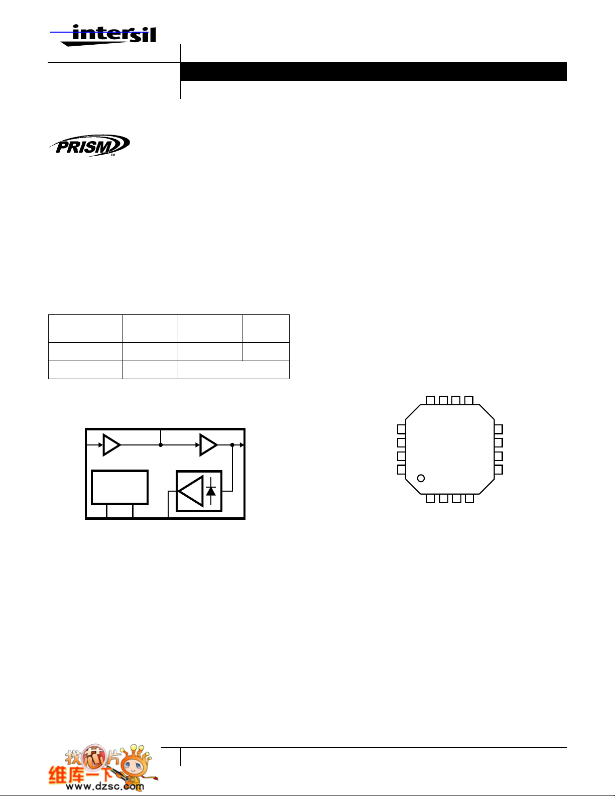
Simplified Block Diagram
DS_VCC
RF_IN
BIAS
PE REXT
PEAK DETECTOR
LOG
DET_OUT
RF_OUT
File Number 4862.4
Features
• Single Supply . . . . . . . . . . . . . . . . . . . . . . . . .2.7V to 3.6V
• Output Power . . . . . . . . . . .18dBm (Typ) at ACPR, DSSS,
1st Side Lobe < -30dBc, 2nd Side Lobe < -50dBc
• Power Gain. . . . . . . . . . . . . . . . . . . . . . . . . . . . 30dB (Typ)
• Detector Linear Input Power Range . . . . . . . . . . . . . .15dB
• Detector Accuracy . . . . . . . . . . . . . . . . . . . . . . . . . . . . . .±1dB
Applications
• IEEE802.11 1, 2 or 5.5Mbps Standard
• Systems Targeting IEEE802.11b, 11Mbps Standard
• Wireless Local Area Networks (WLAN)
• PCMCIA Wireless Transceivers
• ISM Systems Including Automatic Level Control (ALC)
• TDMA Packet Protocol Radios
Pinouts
ISL3984 (MLFP)
TOP VIEW
GND
RF_IN
2
REXT
10
3
DS_VCC
9
4
GND
GND
8
7
6
5
GND
GND
RF_OUT
GND
DET_OUT
VCC_DET
PE
BIAS_GND
GND
12
11
13
PACKAGE PINOUT
14
SUBJECT TO CHANGE
15
16
1
BIAS_VCC
1
1-888-INTERSIL or 321-724-7143 | Intersil and Design is a trademark of Intersil Corporation. | Copyright © Intersil Corporation 2000
CAUTION: These devices are sensitive to electrostatic discharge; follow proper IC Handling Procedures.
PRISM® is a registered trademark of Intersil Corporation. PRISM and design is a trademark of Intersil Corporation.
ISL3984
Pin Descriptions
PIN NUMBER NAME DESCRIPTION
1 BIAS_VCC Power Supply.
2 REXT Bias Resistor, biasing scheme
independent of absolute
temperature.
3 DS_VCC Driver Stage Power Supply.
4, 5 GND DC and RF Ground.
6 RF_OUT RF Outputof thePower Amplifier.
7, 8, 9, 10 GND DC and RF Ground.
11 RF_IN RF Input of the Power Amplifier.
12 GND DC and RF Ground.
13 DET_OUT Detector Output.
14 VCC_DET Detector Power Supply.
15 PE DigitalInput ControlPin toenable
operation of thePower Amplifier.
Enable logic level is high.
16 BIAS_GND DC and RF Ground.
The ISL3984 contains a highly linear RFPA designed to deliver
18dBm and meet an ACPRspecificationof-30dBc in the 2.4 to
2.5GHz ISM band. The performance of this two stage RFPA
can be optimized by adjusting the bias current with a dedicated
resistor. No e xternal positive or negativ e po wer supplies are
required to set the bias currents. The on chip bias network
provides the optimum bias current temperature compensation
when low TC external resistor is used. To get the best
performance from the ISL3984, the output stage matching
network can be tailored using external components.
The ISL3984 power detect function provides a DC output
voltage that is proportional to the logarithm of the output
power. For an output power of 18dBm, the detector is
accurate to within a 0.5dB. The slope of the detector output
voltage is 100mV/dB over a 15dB dynamic range. A simple
application of the detector is to provide in-line monitoring of
the output power using a DC voltmeter. No longer is a power
meter or spectrum analyzer required. A more value added
application would use the HFA3861B/HFA3863 Baseband
Processor to dynamically monitor the ISL3984 output power
and to control transmit power by adjusting the AGC of the
HFA3783 IF Quadrature Modem to provide the best possible
error free data transfer rate for any given environment.
Closed loop power control is very important feature which
compensates for variability in the transmit chain (radio to
radio, channel to channel, over temperature...).
The ISL3984 works seamlessly with the PRISM II and
PRISM II.V WLAN chip set components to give you a highly
integrated, cost effectiv e 11Mb/s WLAN solution in the 2.4 to
2.5GHz ISM band. The ISL3984 is fabricated in the fastest
SiGe BiCMOS process available allo wing superior RF
performance, normally found only in GaAs ICs. Cost effective
functions, normally requiring external components, are
integrated into one IC. The ISL3984 integrates the following
functions in one compact 16 pin MLFP:
• Two Stage, 30dB Gain RFPA,
• Logarithmic power detect function (15dB Dynamic
Range),
• CMOS level compatible Power Up/Down function,
• Single Supply, 2.7V to 3.6V Operation.
The ISL3984 power up/down feature integrates the power
down capability onto the IC and requires no external
components thus freeing up board space and reducing
external component count and cost. When the CMOS
compatible Power Enable (PE) pin is driven low, the total
supply current drops to under 50µA in, typically, 300ns.
When the PE pin is driven high, the full ISL3984 output
power is available in a few hundred nanoseconds.
In summary, the ISL3984 RFPA provides a highly cost
effective solution for the PA function by integrating many
features that would require significant development time,
drive up the total bill of materials cost and consume precious
board space. It mates seamlessly with the other PRISM II
ICs to provide a highly integrated, cost effective 11Mb/s
WLAN solution in the 2.4 to 2.5GHz ISM band.
2
ISL3984
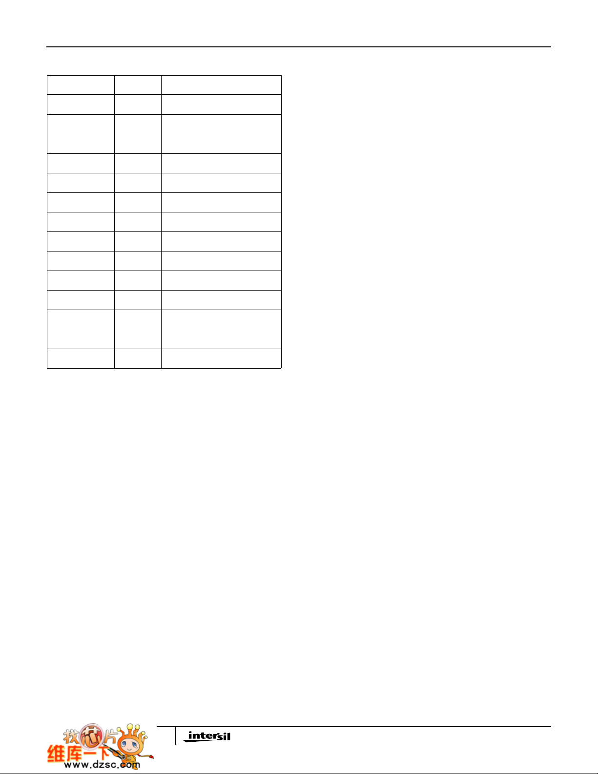
Absolute Maximum Ratings Thermal Information
Supply Voltage. . . . . . . . . . . . . . . . . . . . . . . . . . . . . . . . . . . . . . . .4V
Voltage on Any Other Pin. . . . . . . . . . . . . . . . . . . -0.3 to VCC+0.3V
VCC to VCC Decouple . . . . . . . . . . . . . . . . . . . . . . . . . -0.3 to +0.3V
Any GND to GND. . . . . . . . . . . . . . . . . . . . . . . . . . . . . -0.3 to +0.3V
Operating Conditions
Temperature Range . . . . . . . . . . . . . . . . . . . . . . . . . . . . -40 to 85oC
Supply Voltage Range. . . . . . . . . . . . . . . . . . . . . . . . . . 2.7V to 3.6V
CAUTION: Stresses above those listed in “Absolute Maximum Ratings” may cause permanent damage to the device. This is a stress only rating and operation of the
device at these or any other conditions above those indicated in the operational sections of this specification is not implied.
NOTE:
1. θJAis measured in free air with the component mounted on a high effectivethermalconductivity test board with “direct attach” features. See
Intersil TB379.
General DC Electrical Specifications
PARAMETER TEMP. (oC) MIN TYP MAX UNITS
Supply Voltage Full 2.7 - 3.6 V
Total Power Amplifier Supply Current at 3.3V, 18dBm Output 25 - 137 - mA
RF Detector Supply Current 25 - - 2 mA
Power Down Supply Current Full - 200 - µA
Power Up/ Down Speed Full - 300 - ns
CMOS Low Level Input Voltage Full - - 0.3*V
CMOS High Level Input Voltage (VDD = 3.6V) Full 0.7*V
CMOS Threshold Voltage Full >0.3*V
CMOS High or Low Level Input Current Full -10 - +10 µA
Thermal Resistance (Typical, Note 1) θJA (oC/W)
MLFP Package. . . . . . . . . . . . . . . . . . . . . . . . . . . . . 30
Maximum Junction Temperature (Plastic Package) . . . . . . . .150oC
Maximum Storage Temperature Range. . . . . . . . . . -65oC to 150oC
Maximum Lead Temperature (Soldering 10s) . . . . . . . . . . . . .300oC
V
V
DD
DD
DD
--V
0.5*V
DD
<0.7*V
DD
Power Amplifier AC Electrical Specifications V
PARAMETER TEST CONDITIONS TEMP. (oC) MIN TYP MAX UNITS
RF Frequency Range Full 2400 - 2500 MHz
Power/Voltage Gain Full 27 30 35 dB
Input 50Ω VSWR 25 - - 2:1 Output 50Ω VSWR 25 - - 3:1 Output Power ACPR, DSSS, 1st Side Lobe <-
30dBc, 2nd Side Lobe <-50dBc
Output Stability VSWR Output Spurs Less than -60dBc Full - - 10:1 Output Load Mismatch (Note 2) Full - - 10:1 -
NOTE:
2. Devices sustain no damage when subjected to a mismatch of maximum 10:1.
= 3.3V, f = 2.45GHz, Unless Otherwise Specified. Typical Application Circuit
CC
(external input and output matching networks) has been used.
Full - 18 - dBm
Peak Detector AC Electrical Specifications
TEMP.
PARAMETER TEST CONDITIONS
RF Output Detector Response Time External Capacitor, C = 5pF Full - 0.15 - µs
RF Output Detector Voltage Range Load > 1M Full 0 - 1.5 V
RF Output Detector Linearity Over Linear Range Full -0.5 - 0.5 dB/V
RF Output Detector Accuracy 600mVDC Output Full -1 - +1 dB
(oC) MIN TYP MAX UNITS
RF Output Detector Slope Over Linear Range Full - 10 - dB/V
3

Typical Application Example
L
2
P1
P2
3.3V
D
1
DL4001
BLM31P500S
C
3
0.1µF
DETOUT
V
CC
PE
C
4.7µF
C
9
1000pF
C
6
1000pF
V
CC
1
C
11
270pF
R
100kΩ
ISL3984
ISL3984 - 16 PIN MLFP PACKAGE
10
C
12
11
R
4
1kΩ
R
3
10Ω
2
V
CC
13
14
15
16
C
1000pF
1
2
1
R
4
RFIN (
2.7pF
10
3
4.64kΩ
50Ω)
9
8
7
6
5
4
Typical Performance Curves
-5
-17
-20
2.7V
INPUT RETURN LOSS (dB)
-29
3.6V
1
L
BLM10A1215
V
CC
3
L
1.5nH
C
2
1000pF
L
4
BLM10A1215
-5
-17
-20
INPUT RETURN LOSS (dB)
-29
C
5
1000pF
L
5
2.2nH
25oC
85oC
C
10pF
-40oC
RFOUT (
50Ω)
C
7
8
1.8pF
2.0 3.02.4 2.5
FREQUENCY (GHz)
2.0 3.02.4 2.5
FREQUENCY (GHz)
FIGURE 1. INPUT RETURN LOSS OVER VOLTAGE FIGURE 2. INPUT RETURN LOSS OVER TEMPERATURE
4

Typical Performance Curves (Continued)
ISL3984
-4
-9
OUTPUT RETURN LOSS (dB)
-10
2.0 3.02.4 2.5
FREQUENCY (GHz)
2.7V
3.6V
-4
-40oC
-9
OUTPUT RETURN LOSS (dB)
-10
2.0 3.02.4 2.5
85oC
FREQUENCY (GHz)
25oC
FIGURE 3. OUTPUT RETURN LOSS OVER VOLTAGE FIGURE 4. OUTPUT RETURN LOSS OVER TEMPERATURE
32
30
28
LINEAR GAIN (dB)
3.6V
2.7V
32
30
28
LINEAR GAIN (dB)
-40oC
25oC
85oC
2.0 3.02.4 2.5
FREQUENCY (GHz)
2.0 3.02.4 2.5
FREQUENCY (GHz)
FIGURE 5. LINEAR GAIN OVER VOLTAGE FIGURE 6. LINEAR GAIN OVER TEMPERATURE
0
1
2
OUTPUT POWER (dBm)COMPRESSION (dBm)
-25 -5-11
INPUT POWER (dBm)
3.6V
2.7V
3.6V
2.7V
2dB/DIV.
0
1
2
OUTPUT POWER (dBm)COMPRESSION (dBm)
-25 -5-11
INPUT POWER (dBm)
25oC
85oC
25oC
-40oC
85oC
-40oC
2dB/DIV.
FIGURE 7. GAIN COMPRESSION OVER VOLTAGE FIGURE 8. GAIN COMPRESSION OVER TEMPERATURE
5

Typical Performance Curves (Continued)
2.7V
3V
3.3V
3.6V
ISL3984
-40C
25C
10dB/DIV.
SPAN 50MHz
CENTER FREQUENCY 2450MHz
INPUT POWER -2dBm
10dB/DIV.
SPAN 50MHz
85C
CENTER FREQUENCY 2450MHz
INPUT POWER -2dBm
FIGURE 9. DSSS OUTPUT SIGNAL OVER VOLTAGE FIGURE 10. DSSS OUTPUT SIGNAL OVER TEMPERATURE
0.9
0.8
0.7
0.6
0.5
0.4
0.3
DETECTOR OUTPUT (V)
2.7V
0.2
0.1
0
3.6V
13 14 15 16 17 18 19
OUTPUT POWER (dBm)
20
0.9
0.8
0.7
0.6
o
25
0.5
0.4
0.3
DETECTOR OUTPUT (V)
0.2
0.1
13 14 15 16 17 18 19
C
o
C
-40
OUTPUT POWER (dBm)
o
85
C
20
FIGURE 11. DETECTOR OUTPUT OVER VOLTAGE FIGURE 12. DETECTOR OUTPUT OVER TEMPERATURE
6

Micro Lead Frame Plastic Package (MLFP)
ISL3984
6
0.50 DIA.
0.20
2X
2X
SEATING
PLANE
4X P
4X P
A
1
2
3
B
C
AC0.20
0
C
L
C
L
D
D/2
D1
D1/2
N
TOP VIEW
SIDE VIEW
5
b
D2
D2/2
N
e
(Nd-1)Xe
REF.
BOTTOM VIEW
5
2X
0.25
E1/2
A2
A3
0.10 BAMC
7
1
2
3
E2/2
b
E2
A1
C
E1
A
A
7
A1
E/2
0.05
(Ne-1)Xe
REF.
E
B
0.252XB
C
CC
C
L
L16.4x4
16 LEAD MICRO LEAD FRAME PLASTIC PACKAGE
(COMPLIANT TO JEDEC MO-220-VGGC ISSUE A)
INCHES MILLIMETERS
SYMBOL
A - 0.039 - 1.00
C
A1 - 0.002 - 0.05
A2 - 0.031 - 0.80
A3 0.008 REF 0.20 REF
b 0.009 0.014 0.23 0.35 5
D 0.157 BSC 4.00 BSC
D1 0.147 BSC 3.75 BSC
D2 - 0.088 - 2.25 7
E 0.157 BSC 4.00 BSC
E1 0.147 BSC 3.75 BSC
E2 - 0.088 - 2.25 7
e 0.026 BSC 0.65 BSC
L 0.019 0.029 0.50 0.75
N16 162
Nd 4 4 3
Ne 4 4 3
P 0.009 0.024 0.24 0.60
θ -12-12
NOTES:
1. Dimensioning and tolerancing per ASME Y14.5-1994.
2. N is the number of terminals.
3. Nd isthenumber ofterminals in theX direction, andNe is the
number of terminals in the Y direction.
4. Controlling dimension: Millimeters. Converteddimensions to
inches are not necessarily exact. Angles are in degrees.
5. Dimension b applies to the platedterminal and is measured
between 0.20mm and 0.25mm from the terminal tip.
6. The Pin #1 identifier exists onthetop surface as an
indentation mark in the molded body.
7. Dimensions D2 and E2 arethe maximum exposed pad
dimensions for improved grounding and thermal
performance.
NOTESMIN MAX MIN MAX
Rev. 2 8/00
SECTION "C-C"
e
TERMINAL TIP
FOR ODD TERMINAL/SIDE FOR EVEN TERMINAL/SIDE
e
All Intersil products are manufactured, assembled and tested utilizing ISO9000 quality systems.
Intersil Corporation’s quality certifications can be viewed at website
Intersil products are sold by description only. Intersil Corporation reserves the right to make changes in circuit design and/or specifications at any time without notice.
Accordingly ,the readeris cautioned toverify that data sheets are current before placing orders. Informationfurnished by Intersilis believedto be accurate and reliable.However ,no responsibility is assumed by Intersil or its subsidiaries for its use; nor for any infringements of patents or other rights of third parties which mayresult from its use.
No license is granted by implication or otherwise under any patent or patent rights of Intersil or its subsidiaries.
www.intersil.com/quality/iso.asp.
For information regarding Intersil Corporation and its products, see web site www.intersil.com
7
 Loading...