

Page 1

查询ISL3873A供应商
TM
ISL3873A
Data Sh eet Septemb er 2001
Wireless LAN Integrated Medium Access
Controller with Baseband Processor
The Intersil ISL3873A Wireless LAN
IntegratedMediumAccess Controller
with Integrated Baseband Processor
is part of the PRISM® 2.4GHz radio
chip set. The ISL3873A directly interfaces wi th t he Intersil’s
IF QMODEM (HFA3783).AddingIntersil’sRF/IF Converter
(ISL3685) and Intersil’s Power Amp (HFA3983) offers the
designera completeend-to-endWLAN Chip Set solution.
Protocoland PHY support are implemented in firmwarethus,
supporting customization of the WLAN solution.
Firmware implements the full I EEE 802.11 Wireless LAN
MAC protocol. It supports BSS and IBSS operation under
DCF, and operation under the optional Point Coordination
Function (PCF). Low level protocol functions such as
RTS/CTS generation and acknowledgment,fragmentation
and de-fragmentation, and automatic beacon monitoring are
handled without host intervention. Active scanning is
performed autonomously once initiated by host command.
Host interface command and status handshakes allow
concurrentoperations from multi-threaded I/O drivers.
Additional firmware functions specific to access point
applicationsare also available.
The ISL3873A has on-board A/Ds and D/A for analog I and
Q inputsand outputs, for which the HFA3783IF QMODEM is
recommended. Differential phase shift keying modulation
schemes DBPSK and DQPSK, with data scrambling
capability,are available along with Complementary Code
Keying to provide a variety of data rates. Both Receive and
Transmit AGC functions with 7-bit AGC control obtain
maximum per formance in the analog portions of the
transceiver.
Built-in flexibility allows the ISL3873A to be configured
through a general purpose control bus, for a range of
applications. The ISL3873A is housed in a thin plastic BGA
package suitable for PCMCIA board applications.
The ISL3873A is designed to provide maximum
performancewi th minimum power consumption.Externalpin
layout is organized t o provide optimal PC board layout to all
user interfaces including PCMCIA and USB.
Ordering Information
PART
NUMBER
ISL3873AIK -40 to 85 192 BGA V192.14x14
ISL3873AIK-TK -40 to 85 Tape and Reel 1000 Units/Reel
TEMP.
RANGE (
o
C) PACKAGE
PART
NUMBER
File Number 8015.2
Features
• PCMCIA Host Interface and compatibility with USB V1.1.
• New Start Up Modes Allow the PCMCIA Car d Information
Structure to be Initialized From a Serial EEPROM. This
Allows Firmware to be Downloaded from the Host,
Eliminating the Parallel Flash Memory Device
• Firmware Can be Loaded from Serial Flash Memory
• Zero Glue Connection to 16-Bit Wide SRAM Devices
• Low Frequency Crystal Oscillator to Maintain Time and
Allow Baseband Clock Source to Power off During Sleep
Mode
• Improved Performance of I nternal WEP Engine
• Improvementsto Debug Mode Support Tracing Execution
From on Chip Memory
• Programmable MBUS Cycle Extension Allows Accessing
of Slow Memory Devices Without Slowing the Clock
• Complete DSSS Baseband Processor
• RAKE Receiver with Decision Feedback Equalizer
• ProcessingGain.....................FCCCompliant
• ProgrammableDataRate........1,2,5.5,and11Mbps
• UltraSmallPackage.....................14x14mm
• SingleSupplyOperation ................2.7Vto3.6V
• Modulation Methods. . . .....DBPSK, DQPSK, and CCK
• Supports Full or Half Duplex Operations
• On-Chip A/D and D/A Converters f or I/Q Data (6-Bit,
22MSPS), AGC, and Adaptive Power Control (7-Bit)
• Targetedfor MultipathDelay Spreads 125ns at 11Mbps,
250ns at 5.5Mbps
• Supports Short Preamble and Antenna Diversity
Applications
• PC Card Wireless LAN Adapters
• USB and PCMCIA Wireless LAN Adapters
• PCN / Wireless PBX / Wireless Local Loop
• High Data Rate Wireless LAN Systems Targeting IEEE
802.11b Standard
• Wireless LAN Access Points and Bridge Products
• Spread Spectrum WLAN RF Modems
• TDMA or CSMA Packet Protocol Radios
• PCI Wireless LAN Cards (Using Ext. Br idge Chip)
• ISA, ISA PNP WLAN Cards
Microsoft® and Windows® are registered trademarks of Microsoft Corporation.
PRISM® is a registered trademark of Intersil Americas Inc.
PRISM and design is a trademark of Intersil Americas Inc.
1
CAUTION: These devices aresensitiveto electrostatic discharge;followproperIC Handling Procedures.
1-888-INTERSIL or 321-724-7143 | Intersil andDesign is a trademark of IntersilAmericasInc.
Copyright © Intersil Americas Inc. 2001, All Rights Reserved
Page 2
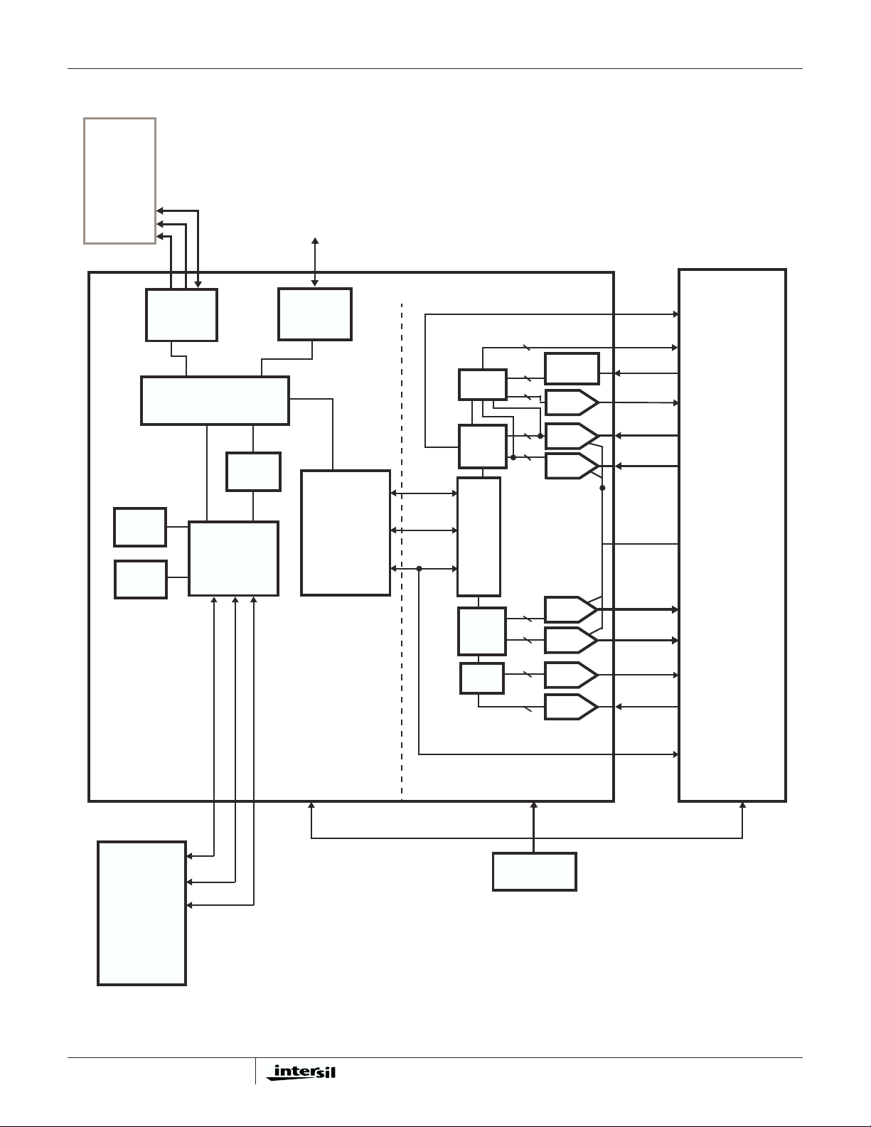
Simplified Block Diagram
HOST
COMPUTER
DATA
ADDRESS
CONTROL
ISL3873A
USB
ON-CHIP
ROM
ON-CHIP
RAM
PC CARD
HOST
INTERFACE
MICRO-
PROGRAMMED
MAC ENGINE
CONTROLLER
WEP
ENGINE
MEMORY
USB
HOST
INTERFACE
INTERFACE
SERIAL
CONTROL
PHY
(MDI)
(MMI)
ISL3873A
DATA I/O
AGC
CTL
DEMOD
I/O
MOD
TX
ALC
PRISM RADIO
ANT_SEL
1
1
DETECT
7
IF
DAC
6
I ADC
6
Q ADC
I DAC
6
6
Q DAC
7
TX
DAC
6
TX
ADC
RX_RF_AGC
RX_IF_DETTHRESH.
RX_IF_AGC
RXI±
RXQ±
V
REF
TXI±
TXQ±
TX_IF_AGC
TX_AGC_IN
RF SECTION
ADDRESS
DATA
SELECT
EXTERNAL
SRAM AND
FLASH
MEMORY
MEDIUM ACCESS
2
CONTROLLER
BASEBAND PROCESSOR
44MHz CLOCK
SOURCE †
†
THE ISL3873A MUST BE SUPPLIED WITHA
SEPARATE CLOCK WHEN USB IS USED.
RADIO AND SYNTH
SERIAL CONTROL
Page 3

ISL3873A
ISL3873A Signal Descriptions
Host InterfaceP ins
PIN NAME PIN I/O TYPE DESCRIPTION
HA0-9 5V tol, CMOS, Input, 50K Pull Down Host PC Card Address Input,Bits 0 to 9
HCE1- 5V tol, CMOS, Input, 50K Pull Up Host PC Card Select, Low Byte
HCE2- 5V tol, CMOS, Input, 50K Pull Up Host PC Card Select, High Byte
HD0-15 5V tol, BiDir, 2mA, 50K Pull Down Host PC Card Data Bus, Bit 0 to 15
HINPACK- CMOS Output, 2mA Host PC Card I/O Decode Confirmation
HIORD- 5V tol, CMOS, Input, 50K Pull Up Host PC Card I/O Space Read Strobe
HIOWR- 5V tol, CMOS, Input, 50K Pull Up Host PC Card I/O Space Write Strobe
HRDY/HIREQ- CMOS Output, 4mA Host PC Card interrupt Request (I/O Mode), also use d as PC Card
HOE- 5V tol, CMOS, Input, 50K Pull Up Host PC Card Memory Attribute Space Output Enable
HREG- 5V tol, CMOS, Input, 50K Pull Up Host PC Card Attribute Space Select
RESET 5V tol, CMOS, ST Input, 50 K Pull Up Hardware Reset. Self-asserted by internal pull-up at power-on. Clock
HSTSCHG- CMOS Output, 4mA Host PC Card Status Change
HWAIT- CMOS Output, 4mA Host Wait, asserted to indicate data transfer not complete and to force
HWE- 5V tol, CMOS Input, 50K Pull Up Host PC Card Memory Attribute Space Write Enable
USB INTERFACE PINS
PIN NAME PIN I/O TYPE DESCRIPTION
USB+ CMOS BiDir, 2mA, (Also USB Transceiver) USB, MBUS Address Bit 20, or I/O as PL5
USB- CMOS BiDir, 2mA, (Also USB Transceiver) USB, MBUS Address Bit 21, or I/O as PL6
USB_DETECT Input, 5V tolerant, pull-down Sense USB VBUS to indicate cable attachment
Ready (Memory Mode) output which is asserted to indicate card
initialization is complete
signal CLKIN or XTALIN must be available before negation of Reset.
Value of MD[15..0] copied to MDIR[15..0] and various control register
bits on the f irst MCLK following releaseof Reset
force host bus wait states
Memory Interface Pins
PIN NAME PIN I/O TYPE DESCRIPTION
MUBE- / MA0 /
MWEH-
MA1-18 CMOS TS Output, 2mA MBUS Address Bits 1 to 18
PL4-MA19 CMOS B iDir, 2mA MBUS Address Bit 19
MLBE- CMOS TS Output, 2mA, 50K Pull Up MBUS Lower Byte Enable, or I/O as PM2
MOE- CMOS TS Output, 2mA MemoryOutputEnable
MWE- / MWEL- CMOS TS Output, 2mA Low (or only) Byte Memory Write Enable
RAMCS- CMOS TS Output, 2mA RAM Select
NVCS- CMOS TS Output, 2mA NV Memory Select
MD0-7 5Vtol, CMOS, BiDir,2mA, 100K Pull Up MBUS Low Data Byte,Bits 0 to 7
MD8-15 5Vt ol, CMOS, BiDir, 2mA
CMOS TS Output, 2mA MBUS Upper Byte Enable for x16 Memory; MBUS Address Bit 0 (byte)
50K Pull-Downs on MD15, MD14, MD13, MD11,
MD10, MD09
50K Pull-Ups MD12, MD08
for x8 Memory; High Byte Write Enable for 2 x8 Memories
MBUS High Data Byte, Bits 8 to 15
Defaultpowerup states are defined by pull-upand pull-down internal
resistors as shown. Device defaults to external EEPROM for boot up
mode. Using external 10K resistors, configure these pins according to
Table 4 to change power-upconfiguration
3
Page 4
ISL3873A
MAC Radio Interface and General Purpose Port Pins
DESCRIPTION OF FUNCTION
PIN NAME PIN I/O TYPE
PJ4 CMOS BiDir, 2mA PE1
PJ5 CMOSBiDir,2mA,50KPullUp LE_IF
PJ6 CMOS BiDir, 2mA LED1
PJ7 CMOS BiDir, 2mA, 50K Pull Up RADIO_PE
PK0 CMOSBiDir,2mA,ST,50KPullDown LE_RF
PK1 CMOS BiDir, 2mA, 50K Pull Down SYNTHCLK
PK2 CMOS BiDir, 2mA, 50K Pull Down SYNTHDATA
PK3 CMOS BiDir, 2mA PA_PE
PK4 CMOS BiDir, 2mA PE2
PK7 CMOS BiDir, 2mA CAL_EN
PL3 CMOS BiDir, 2mA TR_SW_BAR
PL7 CMOSBiDir,2mA,PullDown TR_SW
SERIAL EEPROM PORT PINS
PIN NAME PIN I/O TYPE DESCRIPTION
PJ0 CMOS BiDir SCLK, Serial Clock
PJ1 CMOS BiDir, 50K Pull Down SD, Serial Data Out
PJ2 CMOS BiDir, 50K Pull Down MISO, Serial Data IN
TCLKIN (CS_) CMOS BiDir CS_, Chip Select
Clocks Port Pins
PIN NAME PIN I/O TYPE DESCRIPTION
CLKIN CMOS Input, 50K Pull Down External Clock Input to MCLK prescaler (at >= 2X Desired MCLK
Frequency, Typically 44-48MHz)
XTALIN Analog I nput 32.768kHz Crystal Input
XTALOUT CMOS Output, 2mA 32.768kHz Crystal Output
CLKOUT CMOS, TS Output, 2mA Internal Clock Output (Selectable as MCLK, TCLK, or TOUT0)
BBP_CLK Input BasebandProcessor Clock.The nominal frequency for this clock is
44MHz.This is used internally to generate divideby 2 and 4 for the
transceiverclock
(IF OTHER THAN I/O PORT)
Baseband Processor Receiver Port Pins
PIN NAME PIN I/O TYPE DESCRIPTION
RX_IF_AGC O Analog drive to the IF AGC control
RX_RF_AGC O Drive to the RF AGC stage attenuator.CMOS digital
RX_IF_DET I Analog input to the receive power A/D converter for AGC control
RXI, ± I Analog input to the internal 6-bit A/D of the In-phase received data. Balanced differential 10+/11RXQ, ± I Analog input to the internal 6-bit A/D of the Quadrature received data. Balanced differential 13+/14-
Baseband Processor Transmitter Port Pins
PIN NAME PIN I/O TYPE DESCRIPTION
TX_AGC_IN I Input to the transmitpower A/D converter for transmitAGC control
TX_IF_AGC O Analog drive to the transmit IF power control
TXI ± O TX Spread baseband I digital output data. Data is output atthe chiprate. Balanced differential 23+/24TXQ ± O TX Spread baseband Q digital output data. Data is output at the chip rate. Balanced differential
29+/30-
4
Page 5
ISL3873A
Misc Control Port Pins
PIN NAME PIN I/O TYPE DESCRIPTION
ANTSEL
ANTSEL O The antenna select signalchangesstate as the receiver switches from antenna to
TestMode I/O Factoryleveltest pin. This pin must be pulled low with a 10K resistor.
CompCap1 I Compensation Capacitor
CompCap2 I Compensation Capacitor
CompRes1 I Compensation Resistor
CompRes2 I Compensation Resistor
DBG(0-4) I/O Debug factory test signals. Do not connect
PIN NAME PIN I/O TYPE DESCRIPTION
V
DDA
V
DD
SUPPLY5V Power 5V Tolerant DC Power Supply
V
SSA
V
sub
GND Ground Digital Ground
VREF Input Voltage Reference for A/D’s and D/A’s
IREF Input CurrentReferencefor internalADC and DAC devices. Requires12K resistorto ground.
ST = Schmitt Trigger (Hysteresis), TS = Three-State. Signals ending with “-” are active low.
O The antenna select signalchangesstate as the receiver switches from antenna to
antennaduringthe acquisitionprocessin the antenna diversity mode. This is a
complement for ANTSEL (pin 40) for differentialdrive of antennaswitches
antennaduringthe acquisitionprocessin the antenna diversity mode. This is a
complement for ANTSEL
(pin 39) for differential drive of antenna switches
Power Port Pins
Power DC PowerSupply2.7 - 3.6V (Not HardwiredTogetheron Chip)
Power DC PowerSupply2.7 - 3.6V
Ground Analog Ground
Ground Analog Ground
ISL3873A Pin Number Assignments
PIN NUMBER SIGNAL NAME PIN NUMBER SIGNAL NAME PIN NUMBER SIGNAL NAME PI N NUMBER SIGNAL NAME
A1 NC C7 HD4 F4 MA5 K16 V
DD
A2 MA10 C8 HD6 F13 HD9
A3 MA13 C9 HD14 F14 HD10 L1 MD8
A4 MA16 C10 HD11 F15 HA2 L2 MD7
A5 GND C11 HD7 F16 HA1 L3 MD10
A6 PL4_MA19 C12 HA7 L4 MD9
A7 DBG2 C13 GND G1 MD12 L13 GND
A8 V
DD
A9 HD3 C15 NC G3 V
C14 DBG3 G2 MD14 L14 R X_RF_AGC
DD
L15 ANT_SEL
A10 HCE2 C16 RESET G4 MA2 L16 ANT_SEL
A11 GND G13 GND
A12 HD15 D1 MA3 G14 HSTSCHG M1 MD5
A13 HA9 D2 MA8 G15 HD0 M2 V
A14 V
DD
D3 MA7 G16 BBP_CLK M3 GND
DD
A15 HA6 D4 MA14 M4 MD6
A16 NC D5 MA17 H1 V
DD
M13 V
DDA
D6 DBG0 H2 MLBE M14 COMPCAP1
B1 V
DD
D7 GND H3 MD11 M15 GND
5
Page 6

ISL3873A
ISL3873A Pin Number Assignments (Continued)
PIN NUMBER SIGNAL NAME PIN NUMBER SIGNAL NAME PIN NUMBER SIGNAL NAME PI N NUMBER SIGNAL NAME
B2 NC D8 HD5 H4 MD13 M16 V
B3 MA9 D9 HIREQ H13 HD2
B4 MA12 D10 HIOWR H14 HD1 N1 MD4
B5 V
DD
D11 HOE H15 HA0 N2 MD0
B6 MA18 D12 NC H16 HD8 N3 MD3
B7 DBG1 D13 HA5 N4 MD2
B8 HD12 D14 HWAIT J1 XTALIN N5 NC
B9 HCE1 D15 SUPPLY5V J2 XTALOUT N6 PJ7
B10 V
DD
D16 HREG J3 RAMCS N7 PK2
B11 HIORD J4 NVCS N8 VDDA
B12 HA8 E1 GND J13 USB_DET N9 V
B13 HWE E2 MA4 J14 V
DD
N10 V
B14 HA4 E3 GND J15 USB- N11 V
B15 NC E4 NC J16 USB+ N12 IREF
B16 DBG4 E13 HA3 N13 V
E14 V
DD
K1 CLKIN N14 NC
C1 MA6 E15 HINPACK K2 MOE N15 RX_IF_AGC
C2 NC E1 6 GND K3 MWEL N16 TX_IF_AGC
C3 MA11 K4 GND
C4 MA15 F1 MD15 K13 TESTMODE
C5 CLKOUT F2 MA1 K14 GND
C6 HD13 F3 MWEH_MA0 K15 GND
P1 MD1 R1 PJ1
(SDATA)
P2 PJ2
R2 NC T2 V
(MISO)
T1 PJ0
(SCLK)
DD
P3 TCLKIN R3 NC T3 PJ6
(LED1)
P4 PJ5
(LE_IF)
P5 GND R5 PK0
P6 PL7
(TR_SW)
P7 PK7
R4 PJ4
(PE1)
T4 PK1
(SYNTHCLK)
T5 PK4
(LE_RF)
R6 PK3
(PA_PE)
T6 PL3
(PE2)
(TR_SW_BAR)
R7 RXI+ T7 RXI-
(CAL_EN)
P8 V
DDA
R8 V
DDA
T8 V
DDA
P9 GND R9 RXQ+ T9 RXQP10 V
SUB
P11 VREF R11 V
P12 V
DDA
P13 COMPRES2 R13 COMCAP2 T13 V
R10 RX_IF_DET T10 TX_AGC_IN
DDA
T11 V
SSA
R12 TXI+ T12 TXI-
SSA
P14 N C R14 TXQ+ T14 TXQP15 NC R15 NC T15 COMPRES1
P16 NC R16 NC T16 NC
DD
(RADIO_PE)
(SYNTHDATA)
SSA
SUB
DD
SSA
6
Page 7
ISL3873A
Absolute M axi m um Rati ng s Thermal Information
Supply Voltage, VCC.................................3.6V
Input, Output or I/O Voltage . . . . . . . . . . . .GND -0.5V to V
CC
+0.5V
ESDClassification.................................Class2
Operating Conditions
Voltage...........................................+3.3V
AmbientTemperatureRange...................-40
CAUTION: Stresses above those listed in “Absolute Maximum Ratings” may cause permanent damage to the device. This is a stress only rating and operationofthe
device at these or any other conditions above those indicated in the operational sections of this specification is not implied.
NOTE:
is measured with the component mountedon a low effectivethermalconductivity test boardin free air. See Tech Brief TB379 for details.
1. θ
JA
o
Cto85oC
DC El ectri cal Specifications
PARAMETER SYMBOL TE ST COND ITIONS MIN TYP MAX UNITS
Power Supply Current I
CCOP
Input Leakage Current I
Output Leakage Current I
Logical One Input Voltage V
Logical Zero Input Voltage V
Logical One Output Voltage V
Logical Zero Output Voltage V
Input Capacitance C
Output Capacitance C
OUT
NOTE: All values in this table have not been measured and are only estimates of the performance at this time.
VCC= 3.6V, CLK Frequency 44MHz - - 175 mA
VCC= Max, Input = 0V or V
I
VCC= Max, Input = 0V or V
O
VCC= Max, Min 0.7V
IH
VCC= Min, Max - - 0.3V V
IL
IOH=-1mA,VCC=Min 0.9V
OH
IOL=2mA,VCC=Min - 0.1 0.1V
OL
CLK Frequency 1MHz. All measurements
IN
referenced to GND. T
CLK Frequency 1MHz. All measurements
referenced to GND. T
Thermal Resistance (Typical, Note 1) θ
BGAPackage.............................. 56
MaximumStorageTemperatureRange.......... -65
MaximumJunctionTemperature.......................100
MaximumLead Temperature(Soldering 10s) . . . . . . . . . . . . .300
(Lead Tips Only)
CC
CC
-10 1 10 mA
-10 1 10 mA
CC
CC
--V
--V
CC
-510pF
=25oC
A
-510pF
=25oC
A
(oC/W)
JA
o
Cto150oC
V
o
C
o
C
AC El ectri cal Specifications
PARAMETER SYMBOL MIN TYP MAX UNITS
CLOCK SIGNAL TIMING
OSC Clock Period (Typ. 44MHz) t
High Period t
Low Period t
EXTERNAL MEMORY READ INTERFACE
MOE-Setup Time from RAMCS_ t
MOE_Setup Time from MA (17..0) t
MA(17..1)HoldTimefromMOE_RisingEdge t
RAMCS_ Hold from MOE_ Rising Edge t
MD (15..0) Enablefrom MOE_ Falling t
MO (15..0) Disable from MOE_ RisingEdge t
EXTERNAL MEMORY WRITE INTERFACE
MA ( 17..0) Setup t o MWE_ Falling Edge t
RAMCS_ Setup to MWE t
MA(17..0)HoldfromMWE_RisingEdge t
RAMCS _ Hold from MWE_ Rising Edge t
MD (15..0) Setup to MWE_ Rising Edge t
MD(15..0)HoldfromMWE_RisingEdge t
SYNTHESIZER
SYNTHCLK(PK1) Period t
CYC
H1
L1
S1
S2
H1
H2
E1
D1
S3
S4
H3
H4
S5
H5
CYC
20 20.8 200 ns
10 10.4 - 10 10.4 - -
0--ns
0
-
-ns
20 - - ns
20 - - ns
5
-
-
-
-ns
100 ns
000ns
0--ns
15 - - ns
15 - - ns
40 - - ns
15 - - ns
83 - 4,000 ns
7
Page 8

ISL3873A
AC El ectri cal Specifications (Continued)
PARAMETER SYMBOL MIN TYP MAX UNITS
SYNTHCLK(PK1) Width Hi t
SYNTHCLK(PK1) Width Lo t
H1
L1
SERIAL PORT
SYNTHCLK(PK1) Clock Period t
Low Width t
Delay from Clock Falling Edge to SPCSx, SPAS, SPREAD,
SYNTHDATA(PK2) Outputs
Setup Time of SYTHNDATA(PK2) Read to SYTHNCL K(PK1) F alling Edge t
Hold Time of SYTHNDATA(PK2) Read from SYTHNCLK(PK1) Falling Edge t
Hold Time of SYTHNDATA(PK2) Write from SYTHNCLK(PK1) Falling Edge t
CYC
H1,tL1
t
CD
DRS
DRH
DWH
SYSTEM INTERFACE - PC CARD IO READ 16
Data Delay After HIORD- t
Data Hold Following HIORD- t
HIORD- Width Time t
Address Setup Before HIORD- t
Address Hold Following HIORD- t
HCE(1,2)- Setup Before HIORD- t
HCE(1,2)- Hold After HIORD- t
HREG- Setup Before HIORD- t
HREG- Hold Following HIORD- t
HINPACK- Delay Falling from HIORD- t
HINPACK- Delay Rising from HIORDN d
HWAIT- t
Data Delay from HWAIT- Rising t
HWAIT- Width Time t
DIORD
HIORD
WIORD
SUA
HA
SUCE
HCE
SUREG
HREG
DFINPACK
DRINPACK
DFWT
DRWT
WWT
SYSTEM INTERFACE - PC CARD IO WRITE 16
Data Setup Before HIOWR- t
Data Hold Following HIOWR- t
HIOWRN- Width Time t
Address Setup Before HIOWR- t
Address Hold Following HIOWR- t
HCE(1,2)- Setup Before HIOWR- t
HCE(1,2)- Hold Following HIOWR- t
HREG- Setup Before HIOWR- t
HREG- Hold Following HIOWR- t
HWAIT- Delay Falling from HIOWR- t
HWAIT- Width Time t
HIOWRN High from HWAIT- High t
SUIOWR
HIOWR
WIOWR
SUA
HA
SUCE
HCE
SUREG
HREG
DFWT
WWT
DRIOWR
BASEBAND SIGNALS
Full Scale Input Voltage (V
) 0.25 0.50 1.0 V
P-P
Input Bandwidth (-0.5dB) -20-MHz
Input Capacitance -5-pF
Input Impedance (DC) 5--kΩ
FS (Sampling Frequency) --22MHz
t
/2- 10 - t
CYC
t
/2- 10 - t
CYC
/2+ 10 ns
CYC
/2+ 10 ns
CYC
83ns - 4000 ns
t
/2 -10 - t
CYC
/2 + 10 ns
CYC
-10-ns
15 - - ns
0--
0--
--100ns
0--ns
165 - - ns
70 - - ns
20 - - ns
5--ns
20 - - ns
5--ns
0--ns
0 - 45 ns
30 - 45 ns
- - 35 ns
--0ns
- - 12,000 ns
30 - 92 ns
20 - - ns
165 - - ns
70 - - ns
20 - - ns
5--ns
20 - - ns
5--ns
0--ns
- - 35 ns
- - 12,000 ns
0--ns
8
Page 9
Waveforms
ADDRESS
MA(17..1)
RAMCS_
MOE_
MD(15..0)
ISL3873A
t
H1
t
t
S1
t
S2
t
E1
FIGURE 1. EXTERNAL M EM ORY READ TIMING
H2
t
D1
ADDRESS
MA(17..1)
RAMCS_
MWE_
MD(15..0)
SYNTHCLK
t
H3
t
S4
t
S3
t
S5
t
H4
t
H5
FIGURE 2. EXTERNAL MEM O RY WRITE TIMING
t
H1tL1
t
D3
SYNLE
SPCSPWR
SYNTHDATA
9
t
CYC
t
D1
D[n] D[n-1] D[n -2] D[2] D[1] D[0]
t
D2
FIGURE 3. SYNTHESIZER
Page 10
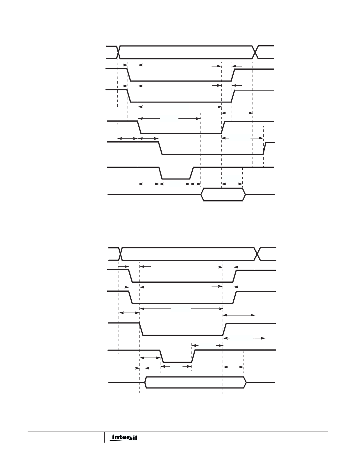
Waveforms (Continued)
HA[15:0]
HREG-
ISL3873A
t
SUREG
t
HREG
HCE(1, 2) -
HIORD-
HINPACK-
HWAIT-
HD[15:0]
HA[15:0]
t
SUA
I
SUCE
t
WIORD
t
DIORD
t
DFINPACK
t
DFWT
t
WWT
FIGURE 4. PC CARD IO READ 16
t
HCE
t
DRWT
t
DRINPACK
t
HIORD
t
HA
t
SUREG
t
HREG
HREGN-
t
t
SUCE
HCE
HCE (1, 2) -
t
SUA
t
WIOWR
t
HA
HIOWR-
t
DRINPACK
t
DRIOWR
HWAIT-
t
SUIOWR
t
DFWT
t
WWT
t
HIOWR
HD[15:0]
FIGURE 5. PC CARD IO WRITE 16
I
10
Page 11
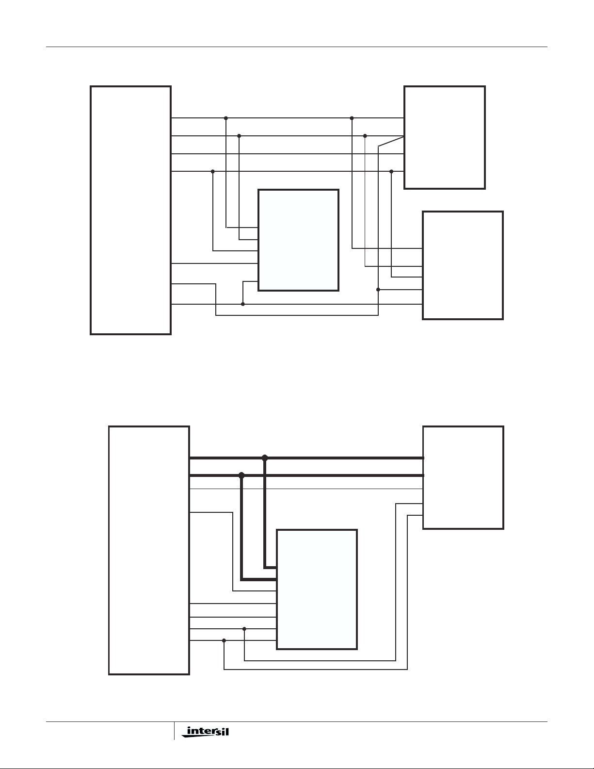
ISL3873A MAC System Overview
ISL3873A
ISL3873A
MA0/MWEH_
RAMCS_
MD0..15
MA1..17
NVCS_
MOE_
SRAM
128Kx8
MD0..7
MA1..17
OE_
MWEL_
WE_
CS_
FIGURE 6. 8-BIT MEMORY INTERFACE REQUIREMENTS FOR ISL3873A
FLASH
128Kx8
MD0..7
MA0..16
CS_
OE_
SRAM
128Kx8
MD8..15
MA1..17
OE_
WE_
CS_
ISL3873A
MA1..17
MD0..15
NVCS-
MA0/MWEH-
SRAM
128Kx16
ADDR(0..16)
DATA(0..15)
UB-
MLBE-
RAMCS-
MOE-
MWEL-
LBCE-
OE
WE
FIGURE 7. 16-BIT MEMORY INTERFACE REQUIREMENTS FOR ISL3873A
FLASH
128Kx16
ADDR(0..16)
DATA(0..15)
CE-
OEWE
11
Page 12
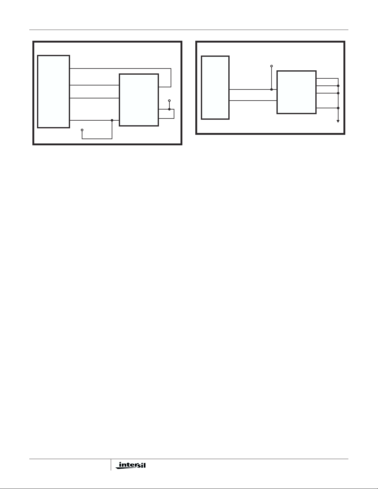
ISL3873A
LARGE SERIAL EEPROM
MISO (PJ2)
SD (PJ1)
ISL3873A
SCLK (PJ0)
CS# (TCLKIN)
PULLUP
SI
SCK
CS
SO
PULLUP
RESET#
WP#
45DB011
FIGURE 8. SERIAL EEPROM INTERFACE
External Memory Interface
The ISL3873A provides separate external chip selects for
code space and data storage space. Code space is
accessibleas data space through an overlay mechanism,
except for an internal ROM. Refer to Figures 6, 7 and 8 for
ISL3873A memory configuration detail examples.
The maximum possible memory space size is 4Mbytes. If
USB is the host i nterface, this is reduced to 1Mbyte.
Most of the data store space is reserved for storage of
receivedand transmitted data,with some areas reserved f or
use by firmware. However,a portion of the data store may be
allocated as code store. This permits higher speed
instruction execution, by using fast RAMs, than is possible
from Flash memories. The maximum size of this overlay is
the full code space address range, 128Kbytes, and is
allocated in independent sections of 16KBytes each, on
16Kbyteboundaries,ranging from the highestaddress of the
actual physical memory space and extending down.
Mapping code execution to RAM requires the RAM to have
code written into it. Typically,this is done by placing code in a
non-volatile memory such as a Flash in the code space. At
initialization, the code in the non-volatile memory transfers itself
to RAM, maps the appropriate blocks of the code space to the
RAM, and then branches to begin execution from RAM. This
allows low cost, slow Flash devices to hold an entire code
image, which can be executed much faster from RAM. If code
is not placed in an external non-volatile memory as described
here, it must be transferred to the RAM via the Host Interface.
Slow memories are not dynamically sensed. Followingreset,
the instructionclock operates with a slower cycle while the
Flash is copied to RAM. Once code has been copied from
Flash to RAM, execution transfers to RAM and the clock is
raised t o the normal operating frequency.
As mentioned above, it is feasible to operate without a code
image in a non-volatile memory. In such a system, the
SMALL SERIAL EEPROM
PULLUP
AO
ISL3873A
NOTE: Must operate at 400kHz AT 3.3V
CS# (TCLKIN)
SCLK (PJ0)
SDA
SCL
24C08 (NOTE)
DC
A1
A2
WP
firmware must be downloaded to RAM through t he host
interface before operation can commence.
The external SRAM memory must be organized in a 16-bit
width t o provide adequate performanceto implement the
802.11 protocol at 11Mb/srates. Systems designed for lower
performanceapplications may be able to use 8-bit wide
memory.
The minimum external memory is 128Kbytes of SRAM,
organized 8 or 16 bits wide. Typical applications, including
802.11 station designs, use 256Kbytes organized 128K x 16.
An access point application could make use of the full address
space of the device with 4Mbytes organized a 2M x 16.
The ISL3873A supports8 or 16-bitcode space, and 8 or 16bit data space. Code space is typically populated with the
leastexpensive Flash memoryavailable, usuallyan 8-bit
device. Data space is usually populated with high-speed
RAMsconfigured as a 16-bit space.This mixing of 8/16 bit
spaces is fully supported, and may be done in any
combination desired for code and data space.
The ISL3873A supports direct control of single chip 16-bit
wide SRAMs with high/low byte enables, as well as direct
controlof a 16-bit space constructed from 8-bit wide SRAMs.
The type of memory configuration is specified via the
appropriate MD pin, sensed when the ISL3873A is reset.
ISL3873A pin MUBE-/MA0/MWEH- functions as Address 0
for 8-bit access, (such as Flash) as M WEH (High Byte Write
Enable) when two x8 memories are configured as a single
x16 space, and as the upper Byte Enable when a single x 16
memory is used. No external logic is required to generate
the required signalsfor both types of memory configurations,
even when both exist together; all that is required is for the
ISL3873A code to configure the ISL3873A memory
controller to generate the proper signals for t he particular
address space being accessed.
12
Page 13

ISL3873A
For 8-bit spaces, the ISL3873A dynamically configures pin
MUBE-/MA0/MWEH- cycle-by-cycle as the address LSB.
MWEL-/MWE-is the only write control,and MOE- is the read
output enable.
For 16-bit spaces constructed from 8-bit memories, the
ISL3873A dynamically configures pin MUBE-/MA0/MWEHcycle-by-cycle as the high byte write enable, MWEL- as the low
write enable signal, and MOE- as the read output enable.
For 16-bit spaces constructedfrom single-chip x16
memories (such as SRAMs), the ISL3873A dynamically
configures pin MUBE_/MA0/MWEH- cycle-by-cycle as the
upper byte enable. Pin MLBE- is connected as the low byte
enable, MWEL-/MWE- is the write control, and MOE- is the
read output enable.
Thesememoryimplementationsrequireno externallogic.The
memory spaces may each be constructed from any type of
memory desired. The only restriction is that a single memory
space must be constructed from the same type of memory; for
example,data space may notuse bothx8 and x16 memories,
it must be all x8, or all x16. This restrictiondoes not apply
across memory spaces; e.g., code space may use a x8
memory and data space a single x16 memory, or code space
two x8 memories and data space a single x8 memory.
Serial EEPROM Interface
The ISL3873A contains a small on-chip ROM firmware which
was added to allow the CIS or CIS plus firmware image to be
transferred from an off-chip serial non-volatile memory device
to RAM after a system reset. This allows a system configuration
without a parallel Flash device. The operating frequency of the
serial port is 400kHz with a voltage of 3.3V .Refer to Figure 8 for
additional details on configuring the serial memory to the
ISL3873A. The Power On Reset Configuration section in this
document provides additional details on memory selection and
control after a Reset condition.
PC Card Interface
PC Card Physical Interface
The Host interface is compatible to the PC Card 95 Standard
(PCMCIA v2.1). The ISL3873A Host Interface pins connect
directly to the correspondingly named pins on the PC Card
connector with no external components (other than resistors)
required. The ISL3873A operates as an I/O card using less
than64 octetlocations. Readsand writesto internal registers
and buffer memory are performed by I/O accesses. Attribute
memory (256 octets) is provided for the CIS table which is
located in external memory. Common memory is not used.
The following describesspecific features of various pins:
HA[9:0]
Decoding of the system address space is performed by the
HCEx-. During I/O accesses HA[5:0] decode the register.
HA[9:6] are ignored when the internal HAMASK register is
set to the defaults used by the standard firmware. During
attribute memory accesses HA[9:1] are used.
HD[15:0]
The host interface is primarily designed for word accesses,
although all byte access modes are fully supported. See
HCE1-, HCE2- for a further description. Note that attribute
memory is specified for and operates with even bytes accesses
only.
HCE1-, HCE2-
The PC Card cycle type and widthare controlled with the CE
signals. Word and Byte wide accesses are supported, using
the combinationsof HCE1-, HCE2-, and HA0 as specified in
the PC Card standard.
HWE-, HOE-
HOE- and HWE- are only used to access attribute memory.
Common Memory,as specified in the PC Card standard, is
not used in the ISL3873A. HOE- is the strobe that enables
an attribute memory read cycle. HWE- is the corresponding
strobe f or the attribute memory wr ite cycle. The attribute
space contains the Card Information Structure (CIS) as well
as the Function Configuration Registers (FCR).
HIORD-, HIOWR-
HIORD- and HIOWR- are the enabling strobes for register
access cycles to the ISL3873A. These cycles can only be
performed once the initializationprocedure is complete and
the ISL3873A has been put into IO mode.
HREG-
This signal must be asserted for I/O or attribute cycles. A
cycle where HREG- is not asserted will be ignored as the
ISL3873A does not support common memory.
HINPACK-
Thissignal isasserted by the ISL3873Awhenever a validI/O
read cycle takes place.A valid cycle is when HCE1-, HCE2-,
HREG-, and HIORD- are asserted, once t he initialization
procedure is complete.
HWAIT-
Waitstates are inserted in accesses using HWAIT-. The host
interface synchronizes all PC Card cycles to the internal
ISL3873A clock. The following wait states should be
expected:
Direct Read or Write to Hardware Register
• 1/2 to 1 MCLK assertion of HWAIT- for internal
synchronization.
Write to Memory Mapped Register, Buffer Access Path,
or Attribute Space (Post-Write)
• The data required for the write cycle will be latched and
therefore only the synchronizing wait state will occur.
• Until the queued cycle has actually written to the memory,
any subsequent access by the Host will result in a WAIT.
13
Page 14

ISL3873A
Read to Attribute Space and Memory Mapped Registers
• WAITwill assert until the memory arbitration and access
have completed.
Buffer Access Paths, BAP0 and BAP1
• Aninternal Pre-Read cycleto memory is initiatedby a host
Buffer Read cycle, after the internal address pointer has
auto-incremented. If the next host cycle is a read to the
same buffer, the data will be available without a memory
arbitrationdelay.
• A single register holds the pre-read data. Thus, any read
accessto any other memory-mappedregister (or the other
buffer access path) will r esult in the pre-read data
becoming invalidated.
• If another read cycle has invalidated t he pre-read, then a
memory arbitration delay will occur on the next buffer
access path read cycle.
HIREQ-
Immediately after reset, the HIREQ- signal serves as the
RDY/BSY (per the PC Card standard). Once the ISL3873A
firmware initialization procedure is complete, HIREQ- is
configured to operate as the interrupt to the PC Card socket
controller. Both Level Mode and Pulse Mode interruptsare
supported. By default, Level m ode i nterrupts are used, so
the interrupt source must be specifically acknowledged or
disabled before the interruptwill be removed.
RESET
When reset is de-asserted, the CIS table is initialized and,
once complete, HIREQ- is set high (HIREQ- acts as
RDY/BSY from reset and is set high to indicate the card is
readyfor use). The CIS tableresides i n Flash memory and is
copied to RAM during firmware initialization. The host
system can then initialize the card by reading the CIS
informationand writing to the configuration register.
ISA PNP
The ISL3873Acan be connected to the ISA bus and operate
in a Plug and Play environment w ith an additional chip such
as the Fujitsu MB86703, Texas Instruments TL16PNP200A,
or Fairchild SemiconductorNM95MS15. See the Application
Note AN9874, “ISA Plug and Play with the HFA3841” for
more details.
Register Interface
The logical view of the ISL3873A from the host is a block of
32 word w ide registers. These appear in IO space starting at
the base address determined by the socketcontroller. There
are three types of registers.
Hardware Registers (HW)
• 1 to 1 correspondence between addresses and r egiste r s.
• No memory arbitration delay, data transfer directly to/from
registers.
• AUX base and offset are write-only, to set up access
through AUX data port.
Note: All register cycles, including hardware registers, incur
a short wait state on the PC Card bus to insure the host
cycle is synchronized with the I SL3873A's internal MCLK.
Memory Mapped Registers in Data RAM (MM)
• 1 to 1 correspondence.
• Requires memory arbitration, since registers are actually
locations in ISL3873A memory.
• Attribute memory access is mapped into RAM as Baseaddress + 0x400.
• AUX port provides host access to any location in
ISL3873A RAM (reserved).
Buffer Access Path (BAP)
• No 1 to 1 correspondence between register address and
memory address (due to indirect access through buffer
address pointer registers).
• Auto increment of pointer registers after each access.
• Require memory arbitrationsince buffers are located in
ISL3873A memory.
• Buffer access may incur additional delay for Har dware
Buffer Chaining.
Buffer Access Paths
The ISL3873A has two independent buffer access paths, which
permits concurrent read and write transfers. The firmware
provides dynamic memory allocation between Transmit and
Receive, allowing efficient memory utilization. On-the-fly
allocation of (128-byte) memory blocks as needed for reception
wastes minimal space when receiving fragments. The
ISL3873A hides management of free memory from the driver,
and allows fast response and minimum data copying for low
latency .The firmware provides direct access to TX and RX
buffers based on Frame ID (FID). This facilitates Power
Management queuing, and allows dynamic fragmentation and
de-fragmentation by the controller.Simple Allocate/De-allocate
commands ensure low host CPU overhead for memory
management.
Hardware buffer chaining provideshigh performance while
reading and writing buffers. Data is transferred between the
host driver and the ISL3873A by writing or reading a single
register location (the Buffer Access Path, or BAP). Each
access increments the address in the buffer memory.
Internally,the firmware allocates blocks of memory as needed
to provide the requested buffer size. These blocks may not be
contiguous, but the firmware builds a linked list of pointers
between them. When the host driver is transferring data
through a buffer access path and reaches the end of a
physical memory block, hardware in the host interface follows
the linked list so that the buffer access path points to the
beginning of the next memory block. This process is
completely transparent to the host driver, which simply writes
or reads all buffer data to the same register. If the host driver
attempts to access beyond the end of the allocated buffer,
subsequentwritesare ignored,and reads will be undefined.
14
Page 15

ISL3873A
FID
ALLOCATE/
DEALLOCATE
REQUEST
OFFSET CENTER
HOST
BUS
DATA PORT
PRE-READ/
POST-WRITE
FIGURE 9. BLOCK DIAGRAM OF A BUFFER ACCESS PATH
BUFFER DESCRIPTOR
ACCESS (FIRMWARE)
BLOCK
OFFSET
USB Port
The USB interface implemented in the ISL3873A Is
compatible with the Universal Serial Bus Specification
Revision 1.1. dated September 23, 1998, which is available
from the USB Implementers’ Forum at http://www.usb.org/
The USB supports 4 endpoints.
• One Communications Class control endpoint for interface
management;
• One Communications Class interrupt endpoint for
signalling interrupts to the host; and,
• Two Bulk endpoints for transfer of encapsulated NDI S
functions to and from the host.
The USB along with USB support firmware provides an
alternate host interface for attaching an 802.11{b} WLAN
adapter t o a host computer. This interface does not provide
“wireless USB” where USB packets are sent on the wireless
medium due to timing constraints in the USB protocol.
USB+ and USB- are the differential pair signals provided for
the user. Thesesignals are capable of directly driving a USB
cable.
USB_DETECT is a 5V tolerantinput to the I SL3873A device.
It is used to signal the MAC processor that a USB cable is
attachedto the unit.
Complete details on the USB firmware for controlling this
port can be obtained by contacting the factory directly.
Power Sequencing
The ISL3873A provides a number of firmwarecontrolledport
pins that are used for controlling the power sequencing and
other functions in t he front end and baseband processor
components of the radio.
Packet transmission requires precise control of the radio.
Ideally, energy at the antenna ceases immediately after the
BUFFER
MEMORY
VIRTUAL
FRAME BUFFER
STA TUS
A
D
HEADER
DATA
last symbol of information has been transmitted while
minimizing spurious radiation. To this end, the
transmit/receive switch is used to smoothly control thepower
output. It's also important to apply appropriatemodulation to
.
the PA while it is active to minimize radiation of CW signals.
Signaling sequences for the beginning and end of normal
transmissions are illustrated in Figure 10. Table 1 lists
applicable delays associated with these control signals.
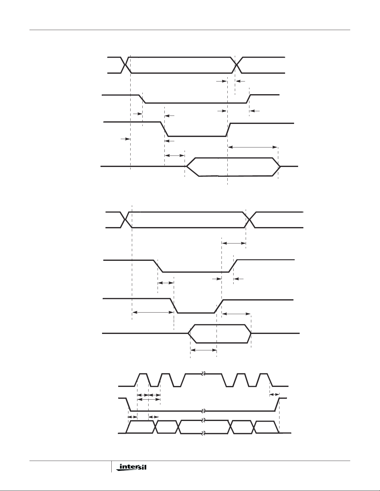
A transmission begins with PE2 and an internal signal
(TX_PE) to the Baseband processor as shown in Figure 10.
This enable activates the transmit state machine in the BBP
and the upconverter in the ISL3783. This starts the
modulated signal flowing to the PA which is turned on by
PA_PE once the drive signal is available. The PA power
ramps up and the power control loop becomes active and
stabilizes. Lastly, the transmit/receive switch is configured
for transmission via the differential pair TR_SW and
TR_SW_BAR. Delays for these signals related to the
initiation of transmission are referenced to PE2. The
switchingof the T/R switch after the PA is enabled is done to
minimizeRF spurious radiation.While it is not usual practice
to switch the T/R switch while RF is on, in this case it
suppresses spurious by employing the 20dB attenuation of
the switch until the PA turn-on or turn-off transients have died.
After the final data bit has been clocked out of the MAC it waits
for an internal control signal (TX_READY) from the Baseband
processor.This signals that the BBP has modulated the final
information-rich symbol. After allowing time for that symbol to
exit the antenna, the MAC de-asserts TR_SW and
TR_SW_BAR to shut off transmission and lowers PA_PE
followed by PE2 going high. Delays for these signals related to
the termination of transmission are referenced to the rising
edge of PE2. The baseband processor also internally extends
the transmission of data bits for a sufficient time to insure that it
outputs the final bits
.
15
Page 16

PE1
PE2
PA_PE
ISL3873A
t
D1
t
D5
t
TR_SW
TR_SW_BAR
FIGURE 10. TRANSMIT CONTROL SIGNAL SEQUENCING
TABLE 1. TRANSMIT CONTROL TIMING SPECIFICATIONS
PARAMETER SYMBOL DELAY TOLERANCE UNITS
PE2toPA_PE t
TPE2 to TR Switch t
TR Switch to PE2 t
PA_PE to PE2 t
D1
D3
D4
D5
0.1 ±0.1 µs
1.5 ±0.1 µs
3 ±0.1 µs
1 ±0.1 µs
D3
PE1 and PE2 encoding details are found in Table 2.
Note that during normal receive and transmit operation that
PE1 is static and PE2 toggles for receive and transmit
states.
TABLE 2. POWER ENABLE STATES
PE1 PE2 PLL_PE
PowerDownState 001
Receive State 1 1 1
TransmitState 101
PLLActiveState 0 1 1
PLL Disable State X X 0
PLL_PE is controlled via the serial interface, and can be used to
disable the internalsynthesizer, t he actual synthesizer control is an
AND function of PLL_PE, and a result of the OR function of PE1
and PE2. PE1 and PE2 will directly control the power enable
functionality of the LO buffer(s)/phase shifter.
Master Clock
Prescaler
The ISL3873A contains a clock prescaler to provide flexibility in
the choice of clock input frequencies. For 11Mb/s operation, the
internal master clock, MCLK, must be at least 11MHz. The
clock generator itself requires an input from the prescaler that is
twice the desired MCLK frequency . Thus the lowest oscillator
frequency thatcan be used for an 11MHzMCLK is 22MHz. The
prescalercan divide by integers and 1/2 steps (IE 1, 1.5, 2, 2.5).
Another way to look at it is that the divisor ratio between the
external clock source and the internal MCLK may be integers
between 2 and 14.
Typically, the 44MHz baseband clock is used as the input, and
the prescaler is set to divide by 2. Contact the factory for further
details on setting the clock prescaler register in the ISL3873A.
t
D4
Low-Frequency Crystal
The ISL3873A MAC controller can accept the same clock signal
as the PHY baseband processor (typically 44MHz), thereby
avoiding the need for a separate, MAC-specific oscillator.The
ISL3873A input has a low-frequency oscillator. This lowfrequency oscillator is intended for use with a 32.768KHz,
tuning-fork type watch crystal to permit accurate timekeeping
with very low power consumption during sleep state.
If a 32.768KHz crystal is connected, the resulting LF clock is
supplied to an intervaltimer to permit measuringsleep
intervalsas well as providinga programmable wake-up time.
In addition, the clock generator can operate either from CLKIN
or (very slowly) from the LF clock. Glitch-free switching
between these two clock sources, under firmware control, is
provided by two, non-architectural Strobe functions (“FAST”
and “SLOW”). In addition, during hardware reset, the clock
generator source is set to the LF clock if no edges are
detected on CLKIN for two cycles of the LF clock (roughly 61
microseconds). This allows proper initialization with omission
of either clocksource, since withoutthe LF crystal attached
there willnot be cycles of the LF clock to activate the detection
circuit. The ability to initialize the ISL3873A using the LF
oscillator to generate MCLK allows the high-frequency (PHY)
oscillator to be powered down during sleep state. If this is
done, firmware can turn on power to the PHY oscillator upon
wake-up, and use the interval timer to measure the start-up
and stabilization period before switching to use CLKIN.
Clock Generator
The ISL3873A can operate with MCLK frequencies up to at
least 12MHz and CLKIN frequencies of at least 50MHz. The
MCLK prescaler generates MCLK (and QCLK) from the
external clock provided at the CLKIN input, or from the output of
the LF oscillator. The MCLK prescaler divides the selected
input clock by any integer value between 2 and 16, inclusive.
• When using a 44MHz CLKIN, as is typical for 802.1 1or
802.11bcontrollers with a PC Card Host Interface, common
divisors are 4 (11MHz) or 5 (8.8MHz)
16
Page 17

ISL3873A
• When using a 48MHz CLKIN, as is typical for 802.11or
802.11b controllers with a USB host i nterface, common
divisors are 4 (12MHz) or 6 (8MHz)
The MCLK prescaler is set to divide by 16 at hardware reset
to allow initializationfirmware to be executed from slow
memory devices at any CLKIN frequency.The MCLK
prescaler generates glitch free output when the divisor i s
Power On Reset Configuration
Power On Reset is i ssued to the ISL3873A with the RESET
pin or via the soft reset bit, SRESET, in the Configuration
Option Register (COR, bit 7). RESET originates from the
HOST systemwhich applies RESET for atleast 0.01ms after
V
has reached 90% of its end value (see PC-Card
CC
standard,Vol. 2, Ch. 4.12.1).
changed. This al lows firmware to change the MCLK
frequency during operation, which is especially useful to
selectively reduce operating speed, thereby conserving
power,when full speed processing is not required.
The MD[15:8] pin values are sampled during RESET or
Software R eset (SRESET). These pins have internal 50K
resistors. External pull-up or pull-down resistors (typically
10kΩ) are used for bits which need to be configured
differently than the default.
XTALIN
XTALOUT
X1
22pF
C1
10MΩ
C2
4700pF
Table 3 summarizes t he effect per pin. Table 4 provides the
MD15 and MD14 bit values required to allow the ISL3873A
to use Serial EEPROM option.
MD[11], StrIdle,has no equivalentfunctionalityin any control
register. When asserted at reset, it will inhibit firmware
execution. This is used to allow the initial download of
firmware in “Genesis Mode”. See the Hardware Reference
FIGURE 11. 32.768kHz CRYSTAL
Manual for more details. The latch is cleared when the
Software R eset, SRESET, COR(7) is active.
TABLE 3. INITIALIZATION STRAPPING OPTIONS ON MBUS DATA PINS
BITS NAME DEFAULT FUNCTION
15:14 NVtype[1:0] 30 Indicates type of serial NV memory to be read by initialization firmware in on-chip ROM.
13 SHIenable 0 Use the Serial Host Interface (USB), and disable all PC Card functions except attribute space, for access to the
12 4Wire 1 Use4-wireinterfaceto SRAM (CS-,OE-,WEH-,WEL-)theISL3873Ax8SRAMs.When = 0selects 5-wireinterface
11 StrIdle 0 Startidle (wait for downloadfrom PC Card host interface).
10 Mem16 0 RAM and NV spaceat startupis x 16. When = 0 RAM and NV space at startup is x 8. If starting from off-chip NV
9 NVds 0 Disable mapping of off-chipcontrol store to NV space (hencemap off-chip control store to RAM space). When = 0
8 ROMds 1 Disable on-chip control store ROM. When = 0 enable on-chip control store ROM.
7 ISAmode 0 Set host interface control signals and address decoding for PC card. When = 1 set host interface signals and
6 FCRinIO 0 Enable I/O space decoding for the physical FCRs. When = 1, the COR, CSR, andPRR registers are accessibleat
5:0 Spare 0 x 00 Not assigned.
a. FCRinIO = 1 forcesHAMASK [0] = 1 to expand I/O space decoding from 0 x 40 to 0 x 80 bytes.
Up to 8NV device types can be encoded with (StrIdle or NVtype). If StrIdle =0, NV memory holds a firmware image,
and NVtype identifies 1 of 4 “large” (. = 128Kb) types. If StrIdle = 1, the NV memory just holds the CIS, and NVtype
identifies 1 of 4 “small” (< = 8Kb) types.
COR and HCR for firmware debugging support. When = 0, use the Parallel Host Interface (PC Card or ISA).
for use with x16 SRAM (CS-, OE-, WE-, UBE-, LBE-).
memorythis setting must indicate the width of the startup Flash Memory. During initialization, firmwarecan set
separate widths or RAM and NV space in the Memory Control Register.
off-chip control store is mapped to NV memory
address decoding is for ISA bus, with all registers in I/O space and attribute space disabled. To use ISA mode,
PHIenable must be = 1 to enable a parallelhost interface.
I/O space offsets 0x40, 0x42, and 0x44 respectively.W hen = 0 these registersare only accessible in attribute
space. This bit is ignored when PHIenable = 0, and is overridden(forced= 1) when ISAmode=1. FCRinIO = 1 is
useful for PC Card operation (PHIenable = 1, ISAmode = 0) to allow non-OS software to access the COR/HCR in
OS environments where the system software does not permit application software to access attribute space.
b
TABLE 4. SERIAL EEPROM SELECTION
MD15 MD14 DEVICE TYPE FUNCTION
0 0 AT45DB011 Large Serial Device used to transfer firmware to SRAM
0 1 24C08 (Note) Small Serial Device which containsonly CIS. MACgoes idle after loading CIS and waits for host.
1 X None Modes not supported in firmwareat this time. Consult factory for additional device typesadded.
NOTE: The operating frequency of the serial port is 400kHz with a voltage of 3.3V.
17
Page 18

ISL3873A
Baseband Processor
The Baseband Processor operation is controlled by the
ISL3873A firmware. Detailed information on programming
the Baseband Processor can be obtain by contacting the
factory.
BBP Packet Reception
The receive demodulatorscrutinizes I and Q for packet
activity. When a packet arrives at a valid signal level the
demodulatoracquires and tracks the incoming signal. It then
sifts through the demodulator data for the Start Frame
Delimiter (SFD). After SFD is detected, The BBP picks off
the needed header fields from the real-time demodulated
bitstream.
Assuming all is well with the header, the BBP decodes the
signal field in the header and switches to the appropriate
data rate. If the signal field is not recognized, or t he CRC16
is in error, the demodulator will return to acquisition mode
looking for another packet. If all is well with the header, and
after the demodulator has switched to the appropriate data
rate, then the demodulator wi ll continue to provide data to
the MAC in the ISL3873A indefinitely.
RX I/Q A/D Interface
The PRISM baseband processor chip (ISL3873A) includes
two 6-bit Analog to Digital converters (A/Ds) that sample the
balanceddifferentialanalog inputfrom the IF down converter
device (HFA3783). The I/Q A/D clock, samples at twice the
chip rate with a nominal sampling rate of 22MHz.
The interfacespecificationsfor the I and Q A/Ds are listed in
Table 5. The ISL3873A is designed to be DC coupled to the
HFA3783.
TABLE 5. I, Q, A/D SPECIFICATIONS
PARAMETER MIN TYP MAX
Full Scale Input Voltage (V
Input Bandwidth (-0.5dB) - 11MHz Input Capacitance (pF) - 2 InputImpedance(DC) 5kΩ --
(Sampling Frequency) - 22MHz -
f
S
The voltages applied to pin 16, V
the references for the internal I and Q A/D converters. In
addition, For a nominal I/Q input of 400mV
suggested V
voltageis 1.2V.
REF
) 0.90 1.00 1.10
P-P
and pin 21, I
REF
,the
P-P
REF
set
AGC Circuit
The AGC circuit as shown in Figure 12 is designed to adjust
for signal level variations and optimize A/D performance for
the I and Q inputs by maintaining the proper headroom on
the 6-bit converters. There are two gain stages being
controlled.At RF, the gain control is a 30dB step change.
This RF gain control optimizes the receiver dynamic range
when the signal level is high and maintainsthe noise figure
of the receiver when it is needed most at low signal level. At
IF, the gain control is linear and covers the bulk of the gain
control range of the receiver.
The AGC loop is partially digital which allows for holding the
gain fixed during a packet. The AGC sensing mechanism uses
a combination of the I and Q A/D converters and the detected
signal level in the IF to determine the gain settings. The A/D
outputs are monitored and controlled in the ISL3873A for the
desired nominal level.
RX_AGC_IN Interface
The signal level in the IF stage is monitored to determine
when to impose the 30dB gain reduction in the RF stage.
This maximizes t he dynamic range of the receiver by
keepingthe RF stages out of saturation at high signal levels.
When the IF circuits’ sensor output r eaches 0.5V
ISL3873A comparatorswitches in the 30dB pad and also
adds 30dB of gain to the IF AGC amplifier. This
compensates the IF AGC and RSSI measures.
DD
,the
TX I/Q DAC Interface
The transmit section outputs balanced differential analog
signals from the transmit DACs to the HFA3783. These are
DC coupled and digitally filtered.
Transmitter Description
The ISL3873A transmitter is designed as a Direct Sequence
SpreadSpectrum Phase Shift Keying (DSSS PSK)
modulator which is capable of handling data rates of up to
11Mbps (refer to AC and DC specifications). The various
modes of the modulator are Differential Binary Phase Shift
Keying (DBPSK) for 1Mbps, Differential Quaternary Phase
ShiftKeying (DQPSK) for 2 Mbps, and Complementary Code
Keying (CCK) for 5.5Mbps and 11Mbps.
CCK is essentially a quadra-phase form of M-ARY Keying. A
description of that modulation can be found in Chapter 5 of:
“Telecommunications System Engineering”, by Lindsey and
Simon, Prentiss Hall publishing. The formula for CCK can be
found later in this datasheet.
The implementeddata rates using a clockrate of 44MHz are
shown in Table 6 and the modulation schemes are indicated
in Figure 13. The major functional blocks of the transmitter
include a Processor Interface, Modulator, Data Scrambler,
Preamble/Header Generator, TX Filter, AGC Control, and
ADC and DAC circuits.Figure 17 provides a basic block
diagram of the DSSS Baseband Processor with an
emphasis on the transmitter section. Figure 19 pr ovides a
basic block diagram of the DSSS Baseband Processor with
an emphasis on the receive section.
The preambleis always transmitted as theDBPSK waveform
while the header can be configured to be either DBPSK, or
DQPSK,anddatapacketscanbeconfiguredforDBPSK,
18
Page 19

ISL3873A
DQPSK,or CCK. The preamble is used by the receiver to
achieve initial Pseudo Noise (PN) synchronization while the
header includes the necessary data fields of the
communications protocol to establish the physical layer link.
The transmitter generates the synchronization preamble and
header and knows when to make the DBPSK to DQPSK or
CCK switchover,as required.
For the 1 and 2Mbps modes, t he transmitteraccepts data
from the external source, scramblesit, differentially encodes
it as eitherDBPSK or DQPSK, and spreads it with the BPSK
PN sequence. The baseband digital signals are then output
to the external IF modulator.
For the CCK modes, the transmitterinputs the data and
partitions it into nibbles (4 bits) or bytes (8 bits). At 5.5Mbps,
it uses four of those bits to select one of 16 complex spread
sequences from a table of CCK sequences. Thus, there are
16 possible spread sequences to send, but only one is sent.
This sequence is then modulated on the I and Q outputs.
The initial phase reference for t he data portion of the packet
is the phase of the l ast bit of the header.At 11Mbps, one
byte is used as above where 8 bits are used to select one of
256 spread sequences for a symbol.
Bit rates for the ISL3873A are defined in Table 6. This table
provides information on bit rates, data rates and symbol
rates f or an MCLK of 44MHz clock. Figure 13 shows the
modulationschemes for the different bits rates. The
modulator is completely independent from the demodulator,
allowing the PRISM baseband processor to be used in full
duplex operation.
Header/Packet Description
The ISL3873A is designed to handle packetized Direct
Sequence Spread Spectrum (DSSS) data transmissions. The
ISL3873A generates its own preambleand header
information. It uses two packet preamble and header
configurations.The firstis backwards compatiblewith the
existing IEEE 802.11-1997 1 and 2Mbps modes and the
secondis the optional shortenedmode whichmaximizes
throughput at the expense of compatibility with legacy
equipment.
In the long preamble mode, the device uses a
synchronization preamble of 128 symbols along with a
header that includes four f ields. The preamble is all 1’s
(before entering the scrambler) plus a Start Frame Delimiter
(SFD). The actual transmitted pattern of the preamble i s
randomized by the scrambler. The preamble is always
transmittedas a DBPSK waveform (1Mbps). The duration of
the long preamble and header is 192µs.
In the short preamble mode, the modem uses a
synchronization field of 56 zero symbols along wi th an SFD
transmitted at 1Mbps. The short header is transmitted at the
2Mbps rate. The synchronizationpreamble is all 0’s to
distinguishit from the long header mode and the short
preambleSFD is the time reverse of the long preamble SFD.
The duration of the short preamble and header is 96µs.
Start Frame Delimiter (SFD) Field (16 Bits)
This field is used to establish the link frame timing. The
ISL3873A will not declare a valid data packet, even if it PN
acquires, unless it detects the SFD. The ISL3873A receiver
auto-detects if the packet is long or short preamble and sets
SFD time-out. The timer starts counting afterinitialization of
the de-scrambler is complete.
RX_RF_AGC
RX_IF_DET
RX_IF_AGC
RX_I±
HFA3683 HFA3783
FIGURE 12. AGC CIRCUIT
TABLE6. BIT RATE TABLE EXAMPLES FOR MCLK = 44 MHz
DATA
MODULATION
DBPSK 22 00 00 1 1
DQPSK 22 01 01 2 1
CCK 22 10 10 5.5 1.375
CCK 22 11 11 11 1.375
A/D SAMPLE CLOCK
(MHz)
TX SETUP CR 5
BITS 1, 0
RX_Q±
THRESH.
DETECT
DAC
I ADC
Q ADC
ISL3873A
RX SIGNAL CR 63
BITS7, 6
1
1
AGC
7
IF
CTL
6
DEMOD
6
I/O
DATA I/O
DATA RATE
(Mbps)
19
SYMBOL RATE
(MSPS)
Page 20

ISL3873A
DATA
I
OUT
Q
OUT
CHIP
RATE
SYMBOL
RATE
I vs. Q
802.11 DSSS BPSK 802.11 DSSS QPSK
1Mbps
BARKER
1 BIT ENCODED TO
ONE OF 2 CODE
WORDS
(TRUE-INVERSE)
11 CHIPS
11 MC/S 11 MC/S
1MS/S 1MS/S
2 BITS ENCODED
TO ONE OF
4 CODE WORDS
2Mbps
BARKER
11 CHIPS
FIGURE 13. MODULATION MODES
5.5Mbps CCK
COMPLEX
SPREAD FUNCTIONS
4 BITS ENCODED
TO ONE OF 16
COMPLEX CCK
CODE WORDS
8 CHIPS
11 MC/S
1.375 MS/S
11MbpsCCK
COMPLEX
SPREAD FUNCTIONS
8 BITS ENCODED
TO ONE OF 256
COMPLEX CCK
CODE WORDS
8CHIPS
11 MC/S
1.375 MS/S
PREAMBLE (SYNC)
128/56 BITS
Start FRAME DELIMITER
16 BITS
PREAMBLE
SIGNAL FIELD
8BITS
FIGURE 14. 802.11 PREAMBLE/HEADER
Header Field
The header field is defined by four fields which are shown in
Figure 14. These fields are Signal Field, Service Field,
Length Field and CITT-CRC16 Field. They are further
defined by the following:
Signal Field (8 Bits) - This field indicates what data rate t he
data packet that follows the header will be. The ISL3873A
receiver looks at the signal field to determine whether it
needs to switch from DBPSK demodulation into DQPSK, or
CCK demodulation at the end of the preamble and header
fields.
Service Field (8 Bits) - TheMSBofthisfieldisusedto
indicate the correct length when the length field value is
ambiguous at 11Mbps. See IEEE STD 802.11 for definition
of the other bits. Bit 2 is used by the ISL3873A to indicate
that the carrier reference and the bit timing references are
derived from t he same oscillator (locked oscillators).
Length Field (16 Bits) - This field indicates the number of
microsecondsit will take to transmit the payload data
(PSDU). The external controller (MAC) will check the length
field in determining when it needs to de-assert RX_PE.
SERVICE FIELD
8BITS
LENGTHFIELD
16 BITS
HEADER
CRC16
16 BITS
CCITT - CRC 16 Field (16 Bits) - This field includes the
16-bit CCITT - CRC 16 calculationof the three header fields.
This value is compared with the CCITT - CRC 16 code
calculated at the receiver. The ISL3873A receiver will
indicate a CCITT - CRC 16 error via CR24 bit 2 and w ill
lower MD_RDY and reset the r eceiver to the acquisition
mode if there is an er ror.
The CRC or cyclic Redundancy Check is a CCITT CRC-16
FCS (FrameCheck Sequence).It is the ones complementof
the remainder generated by the modulo 2 division of the
protectedbits by the polynomial:
16+x12+x5
x
+1
The protected bits are processed in transmit order. All CRC
calculationsare made ahead of data scrambling. A shift
register with tw o taps is used for the calculation. It is preset
to all ones and then the protected fields are shifted through
the register. The output is then complemented and the
residual shifted out MSB first.
The following Configuration Registers (CR) are used to
program the preamble/header functions,more programming
details about these registers can be found in the Control
Registers section of this document:
20
Page 21

ISL3873A
CR 3 - Defines the short preamble length minus the SFD in
symbols.The 802.11 protocol requiresa setting of 56d = 38h
for the optional short preamble.
CR 4 - Defines the long preamble length minus the SFD in
symbols. The 802.11 protocol requires a setting of
128d = 80h for the mandatory long preamble.
CR 5 B its 0, 1 - These bits of the register set the Signal field
to indicate what modulation is to be used for the data portion
of the packet.
CR 6 - The value to be used in the Service field.
CR 7 and 8 - Defines the value of the transmit data length
field. This value i ncludes all symbols following the last
header field symbol and is in microseconds required to
transmitthe data at the chosen data rate.
The packetconsists ofthe preamble, header and MAC Protocol
Data Unit (MPDU). The data is transmitted exactly as received
from the control processor .Some dummy bits will be appended
to the end of the packet to ensure an orderly shutdown of the
transmitter.This prevents spectrum splatter. At the end of a
packet, the external controller is expected to de-assert the
TX_PE line to shut the transmitter down.
Scrambler and Data Encoder Description
The modulator has a data scrambler that implements t he
scrambling algorithm specified in the IEEE 802.11 standard.
This scrambler is used for the preamble, header, and data in
all modes. The data scrambler is a self synchronizingcircuit.
It consists of a 7-bit shift register with feedback from
specified taps of the r egister. Both t ransmitter and receiver
use the same scrambling algorithm. The scrambler can be
disabledbysettingCR32bit2to1.
NOTE: Be advised that the IEEE 802.11 compliant scrambler in the
ISL3873A has the property that it can lock up (stop scrambling) on
random data followed by repetitive bit patterns. The probability of this
happening is 1/128. The patterns that have been identified are all
zeros, all ones, repeated 10s, repeated 1100s,and repeated 111000s.
Any break in the repetitive pattern will restart the scrambler. Toensure
that this does not cause any problem, the CCK waveform uses a ping
pong differential coding scheme that breaks up repetitive 0’s patterns.
Scramblingis done by division with a prescribed polynomial
as shown in Figure 15. A shift register holds the last quotient
and the output is the exclusive or of the data and the sum of
tapsin the shift register. The transmit scrambler seed for the
long preamble or for the short preamble can be set with
CR48 or CR49.
SERIAL
Z-5Z-6Z
DATA OUT
-7
SERIAL DATA
IN
XOR
FIGURE 15. SCRAMBLING PROCESS
Z-1Z-2Z-3Z
-4
XOR
For the 1Mbps DBPSK data rates and for the header in all rates
using the long preamble, the data coder implements the
desired DBPSK coding by differential encoding the serial data
from the scrambler and driving both the I and Q output
channels together.For the 2Mbps DQPSK data rate and for the
header in the short preamble mode, the data coder implements
the desired coding as shown in the DQPSK Data Encoder
Table 7. This coding scheme results from differential coding of
dibits(2 bits).Vectorrotationis counterclockwise although bits 6
and 7 of configuration register CR 1 can be used to reverse the
rotation sense of the TX or RX signal if desired.
Spread Spectrum Modulator Description
Themodulator is designedto generateDBPSK, DQPSK, and
CCK spread spectrum signals. The modulator is capable of
automatically switching its rate where the preamble is
DBPSK modulated, and the data and/or header are
modulated differently. The modulator can support date rates
of 1, 2, 5.5 and 11Mbps. Quadraphase ( I/Q) m odulation is
used at the baseband for all m odulation modes. Further
informationon the programming details required to set up
the modulator can be obtained by contacting the factory.
TABLE 7. DQPSK DATA ENCODER
PHASE SHIFT
000
+90 01
+180 11
-90 10
DIBIT PATTERN (d0, d1)
d0 IS FIRST IN TIME
In the 1Mbps DBPSK mode, the I and Q Channels are
connected together and driven with the output of the scrambler
and differential encoder. The I and Q Channels are then both
multiplied with the 11-bit Barker word at the spread rate. The I
and Q signals go to the Quadrature upconverter (HFA3724) to
be modulated onto a carrier.Thus, the spreading and data
modulation are BPSK modulated onto the carrier.
For the 2Mbps DQPSK mode, t he serial data i s formed into
dibits or bit pairs in the differentialencoder as detailed
above. One of the bits from the differential encoder goes to
the I Channel and the o ther to the Q Channel. The I and Q
Channels are then both multiplied with the 11-bit Barker
word at the spread rate. This forms QPSK modulation at the
symbol rate with BPSK modulation at the spread rate.
CCK Modulation
For the CCK modes, the spreading code length is 8 complex
chipsand based on complementary codes. The chipping rate is
1 1Mchip/s.The following formula is used to derive the CCK
code words that are used for spreading both 5.5 and 11Mbps:
j ϕ
+++()
1ϕ2ϕ3ϕ4
=
ce
j ϕ
+()ej ϕ1ϕ2ϕ
1ϕ4
e
++()
(LSB to MSB), where c is the code word.
j ϕ
++()
1ϕ3ϕ4
e
,,
j ϕ
+()ej ϕ1ϕ2+()ejϕ
3
1ϕ3
e
j ϕ
++()
1ϕ2ϕ4
e
,–,,,–
,
1
21
Page 22

ISL3873A
The terms: ϕ1, ϕ2, ϕ3, and ϕ4 are defined below for
5.5Mbps and 11Mbps.
This f ormula creates 8 complex chips (LSB to MSB) that are
transmittedLSB first.The coding is a form of the generalized
Hadamard transform encoding where the phase ϕ1 is added
to all code chips, ϕ2 is added t o all odd code chips, ϕ3is
added to all odd pairs of code chips and ϕ4 is added to all
odd quads of code chips.
The phase ϕ1 modifies the phase of all code chips of the
sequence and is DQPSK encoded for 5.5 and 11Mbps.This
will take the form of rotating the whole symbol by the
appropriate amount relative to the phase of the preceding
symbol. Note that the last chip of the symbol defined above
is the chip that indicates the symbol’s reference phase.
For the 5.5Mbps CCK mode, the output of the scrambler is
partitioned into nibbles. The first two bits are encoded as
differential symbol phase modulation in accordance with T abl e
8. All odd numbered symbols of the MPDU are given an extra
180 degree (π) rotation in addition to the standard DQPSK
modulation as shown in the table. The symbols of the MPDU
shall be numbered starting with “0” for the first symbol for the
purposes of determining odd and even symbols. That is, the
MPDU starts on an even numbered symbol. The last data dibit
(d2 and d3) CCK encodes the chips as specified in T able9.
This table is derived from the CCK formula above by setting ϕ2
=(d2*pi)+pi/2,ϕ3= 0, and ϕ4 = d3*pi. In Table9 d2 and d3 are
in the order shown and the complex chips are shown LSB to
MSB (left to right) with LSB transmitted first.
TABLE 8. DQPSK ENCODING TABLE
EVEN SYMBOLS
DIBIT PA TTERN (d(0), d(1))
d(0) IS FIRST IN TIME
00 0
01 π/2 3π/2 (-π/2)
11
10 3
TABLE 9. 5.5Mbps CCK ENCODING TABLE
d2, d3 CHIPS
00 1j 11j -1 1j 1-1j 1
01 -1j -1 -1j 11j 1-1j 1
10 -1j 1-1j -1 -1j 11j 1
11 1j -1 1j 1-1j 11j 1
PHASE CHANGE
(+j
ω)
π
π/2 (-π/2) π/2
ODD SYMBOLS
PHASE CHANGE
(+j
ω)
π
0
At 11Mbps, 8 bits (d0 to d7; d0 first in time) are transmitted
per symbol.
The first dibit (d0, d1) encodes the phase ϕ1 based on
DQPSK. The DQPSK encoder is specified in Table 8 above.
The phase change for ϕ1 i s relative to t he phase ϕ1ofthe
preceding symbol. In the case of rate change, the phase
change for ϕ1 is relative to the phase ϕ1 of the preceding
CCK symbol. All odd numbered symbols of the MPDU are
givenan extra180 degree (π) rotation in accordancewith the
DQPSK modulationas shown in Table 8. Symbol numbering
starts with “0” for the first symbol of the MPDU.
The data dibits: (d2, d3), (d4, d5), (d6, d7) encode ϕ2, ϕ3,
and ϕ4 respectively based on QPSK as specified in Table
10. Note that this table is binary, not Grey, coded.
Transmit Filter Description
T ominimize the requirements on the analog transmit filtering,
the transmitsectionshown in Figure 17 has an output digital
filter.This filter is a Finite Impulse Response (FIR) style filter
whose passband shape is set by tap coefficients. This filter
shapes the spectrum to meet the radio spectral mask
requirements while minimizing the peak to average amplitude
on the output. Tomeet the particular spread spectrum
processing gain regulatory requirements in Japan on channel
14, an extra FIR filter shape has been included that has a
wider main lobe. This increases the 90% power bandwidth
from about 11MHz to 14MHz. It has the unavoidable side
effectof increasingtheamplitudemodulation,so theavailable
transmit power is compromised by 2dB when using this filter
(CR 11 bit 5).
TABLE 10. QPSK ENCODING TABLE
DIBIT PATTERN (d(i), d(i+1))
d(i) IS FIRST IN TIME PHASE
00 0
01
10
11 3π/2 (-π/2)
π/2
π
TX Power Control
The transmitter power can be controlled via two registers.
The first register, CR58, contains the results of power
measurements digitizedby the ISL3873A.By comparingthis
measurement to what is needed for transmit power, a
determinationis made whether to raise or lower the transmit
power.It does this by writing the power level desired to
register CR31.
Clear Channel Assessment (CCA) and
Energy Detect (ED) Description
The Clear Channel Assessment (CCA) circuit implements the
carrier sense portion of a Carrier Sense Multiple Access
(CSMA) networking scheme. The Clear Channel Assessment
(CCA) monitors the environment to determine when it is clear
to transmit. The CCA circuit in the ISL3873A can be
programmed to be a function of RSSI (energy detected on the
channel), CS1, SQ1, or various combinations. The CCA is
used by the Media Access Controller (MAC) in the ISL3873A.
The MAC decides on transmission based on traffic to send
and the CCA indication. The CCA indicationcan be ignored,
allowing transmissions independent of any channel
conditions. The CCA in combination with the visibility of the
various internal parameters (i.e., Energy Detection
22
Page 23

ISL3873A
measurement results), can assist the MAC in executing
algorithms that can adapt to the environment. These
algorithms can increase network throughput by minimizing
collisions and reducing transmissions liable to errors.
Thereare three measuresthat can be used in the CCA
assessment. The Receive Signal Strength Indication (RSSI)
which indicates the energy at the antenna, CS1 and carrier
sense (SQ1). CS1 becomesactive anytimethe AGC portion
of the circuit becomes unlocked, which is likely at the onset of
a signalthat is strongenoughto support 11Mbps,but maynot
occur with the onset of a signal that is only strong enough to
support 1 or 2MBps. CS1 stays active until the AGC locks and
a SQ1 assessment is done, if SQ1 is false, then CS1 is
cleared, which deasserts CCA. If SQ1 is true, then tracking is
begun, and CCA continues to show the channel busy.CS1
may occur at any time during acquisition as the AGC state
machine runs asynchronously with respect to slot times.
SQ1 becomes active only when a spread signal with the
properPN code has been detected, and the peak correlation
amplitude to sidelobe ratio exceeds a set threshold, so it
may not be adequate in itself.
A SQ1 evaluation occurs whenever the AGC has remained
locked for the entire data ingest period. When this happens,
SQ1 is updated between 8 and 9µs into the 10µsdwell.If
CS1 is not active, two consecutive SQ1’s are required to
advance the part to tracking.
The state of CCA is not guaranteed from the time RX_PE
goes high until the first CCA assessment is made.At the end
of a packet, after RXPE has been deasserted, the state of
CCA is also not guaranteed.
The Receive Signal Strength Indication (RSSI) measurement is
derived from the state of the AGC circuit. ED is the comparison
result of RSSI against a threshold. The threshold may be set to
an absolute power value, or it may be set to be N dB above the
measured noise floor. See CR 35. The ISL3873A measures
and stores the RSSI level when it detectsno presence of BPSK
or QPSK signals. The average value of a 256 value buffer is
taken to be the noise floor.Thus, the value of the noise floor will
adapt to the environment. A separate noise floor value is
maintained for each antenna. An initial value of the noise floor
is established within 50µs of the chip being active and is refined
as time goes on. Deasserting RX_PE does not corrupt the
learned values. If the absolute power metric is chosen, this
threshold is normally set to between -70 and -80dBm.
Ifdesired,EDmaybeusedintheacquisitionprocessaswell
as CCA. ED may be used to m ask ( squelch) weak signals
and prevent radio reception of signals too weak to support
the high data rates, signals from adjacent cells, networks, or
buildings. See CR 47 (bit 6).
The Configuration registers effecting the CCA algorithm
operationare summarizedbelow ( more programmingdetails
on these registers can be found under the Control Registers
section of t his document).
The CCA output from pin 60 of the device can be defined as
active high or active low through CR 1 (bit 2).
CR9(6:5) allows CCA to be programmed to be a function of ED
only,the logical operation of (CS1 OR SQ1), the logical function
of(EDAND(CS1ORSQ1)),or(EDOR(CS1ORSQ1)).
CR9(7) lets the user select from sampled CCA mode, which
means CCA will not glitch, is updated once per symbol and is
valid for reading at 15.8µs or 18.7µs. In non-sampled mode,
CCA may change at any time, potentially several times per slot,
as ED and CS1 operate asynchronously to slot times.
In a typical system CCA willbe monitoredto determinewhen
the channel is clear.Once the channel is detected busy,
CCA should be checked periodically to determine if the
channel becomes clear. Once MD_RDY goes active, CCA
should be ignoredfor the remainder of the message. Failure
to monitor CCA until MD_RDY goes active (or use of a timeout circuit) could resultin a stalledsystem as it is possible for
the channel to be busy and then become clear without an
MD_RDY occurring.
AGC Description
The AGC system consists of the 3 chips handling the receive
signal, the RF to IF downconverter HFA3683, the IF to
baseband converter HFA3783, and the baseband processor
(BBP) section of the ISL3873A. The AGC loop (Figure 12) is
digitally controlled by the BBP. Basically it operates as follows:
Initially, the receiver is set for high gain. The percent of time
that the A/D converters in the baseband processor are
saturated is monitored along with signal amplitude and the
gain is adjusted down until the amplitude is what will
optimize the demodulator’s performance. If the amount of
saturation is great, the initial gain adjust steps are large. If
the signal overload is small, they are less. When the gain is
about right and the A/Ds’ outputs are within the lock window
(CR19), the BBP declares AGC lock and stops adjusting for
theduration of the packet.If the signal level then varies more
than a preset amount (CR20, CR29), the AGC is declared
unlocked and the gain again allowed to readjust.
The BBP looks for the l ocked state following an unlocked
state(CS1) as one indication that a received signal is on the
antenna. This startsthe receive process of looking for PN
correlation(SQ1). Once PN correlation and AGC lock are
found, t he processor begins acquisition.
For large signals, t he power level in the RF stage out put is
also monitored and if i t is large, the LNA stage is shut down.
This removes 30dB of gain from the r eceive chain which is
compensated for by replacing 30dB of gain in the IF AGC
stage. There is some hysteresis i n this operation and once
the AGC locks, it is locked as well. This improves the
receiver dynamic range.
23
Page 24

ISL3873A
RX_RF_AGC Pad Operation
30dB Pad Engaging (RF Chip Low Gain):
If the AGC is not locked onto a packet, a '1' on the
ifCompDet input will engage in the 30dB attenuation pad.
This causes the AGC to go out of lock and also forces t he
attenuation accumulator to be set to the programmed value
of CR27. The AGC t hen attempts to lock on the signal.
If the AGC is l ocked on a packet, ifCompDet is ignored.
30DB PAD RELEASING (RF CHIP HIG H GAIN):
If the AGC is not locked onto a packet and the attenuation
accumulator sum falls below the programmable threshold
(CR27), the pad will release. This is for the case where a
noise spike kicked in the 30dB pad and the pad should
release when the noise spike ends. Since the noise floor is
different for different environments, it is possible that in some
cases CR27’s programmed value will be below the noise floor
and the pad will not be removed except by RXPE going low.
There is a recommended value to program CR27 (24dB), but
that depends on what environment the radio is in.
During a packet (after AGC lock), the 30dB pad is held
constantand the CR27 threshold is ignored.
RXPE low forces the pad to release whether in the middle of
a packet or not. At the end of a packet,RXPE always goes
low,forcingthepadtorelease.
Notes: The attenuation accumulator is basically about equal to
the current RSSI value.
The accumulator output, after going through the interpolator
lookup table, feeds the AGC D/A.
The value used to represent the pad is programmable
(CR17), but is recommended to be set to 30dB.
ifCompDet is a signalfrom the HFA3783 chip. A '1'indicates
its inputs are near saturation and i t needs the RF chip to
switch f rom high gain to low gain.
RX_IF_Det i s the input to the ISL3873A chip which is
connected to ifCompDet on the HFA3783.
RX_RF_AGC is the output of the ISL3873A chip and '1' is
high gain, '0' is low gain.
Demodulator Description
The receiver portion of the baseband processor, performs A/D
conversionand demodulation of the spread spectrum signal.
It correlates the PN spread symbols, then demodulates the
DBPSK, DQPSK, or CCK symbols. The demodulator includes
a frequency tracking loop that tracks and removes the carrier
frequency offset. In addition, it tracks the symbol timing, and
differentially decodes and descrambles the data. The data is
output through the RX Port to the external processor.
The PRISM baseband processor in the ISL3873A uses
coherent demodulation. The ISL3873A is designed to
achieve rapid settling of the carrier tracking loop during
acquisition.Rapid phase fluctuations are handled with a
relatively wide loop bandwidth which i s then stepped down
as the packet progresses. Coherent processing improves
the BER performance margin as opposed to differentially
coherent processing for the CCK data rates.
The baseband processor uses time invariant correlation to
strip the Barker code spreading and phase processing to
demodulate the r esulting signals in the header and
DBPSK/DQPSK demodulation modes. These operations ar e
illustrated in Figure 18 which is an overall block diagram of
the receiver processor.
In processing the DBPSK header, input samples from the I and
Q A/D converters are correlated to remove the spreading
sequence. The peak position of the correlation pulse is used to
determine the symbol timing. The sample stream is decimated
to the symbol rate and corrected for frequency offset prior to
PSK demodulation. Phase errors from the demodulator are fed
to the NCO through a lead/lag filter to maintain phase lock. The
carrier is de-rotated by the carrier tracking loop. The
demodulated data is differentially decoded and descrambled
before being sent to the header detection section.
In the 1Mbps DBPSK mode, data demodulation is performed
the same as in header processing. In t he 2Mbps DQPSK
mode, the demodulator demodulates two bits per symbol
and differentially decodes these bit pairs. The bits are then
serializedand descrambled prior to being sent t o the output.
In the CCK m odes, the receiver removes carrier frequency
offsets and uses a bank of correlators to detect the
modulation. A biggest picker finds the largest correlation in
the I and Q Channels and determines the sign of those
correlations. For this to happen, the demodulator must know
the starting phase which is determined by referencing the
data to the last bit of the header. Each symbol demodulated
determines1 or 2 nibbles of data. This is then serialized and
descrambled before being passed to the output.
Carrier tracki ng is via a lead /lag filter using a di gital Costas
phase d etect or. C hi p tracking in the CCK modes is chip
decision di rect ed or slaved to the carrier t racki ng
depending on whether or not the locked oscillator desig n is
utilized in the radio.
Acquisition Description
A projected worst case time line for the acquisition of a
signal with a short preamble and header is shown. The
synchronization part of the preamble is 56 symbols long
followed by a 16-bit SFD. The receiver must monitor the
antenna to determine if a signal is present. The timeline is
broken into 10µs blocks (dwells) for the scanning process.
This length of time is necessary to allow enough integration
of the signal to make a good acquisition decision.This worst
case time line example assumes that the signal arrives part
way into the first dwell such as to just barely catch detection.
The signal and the scanning process are asynchronous and
the signal could start anywhere. I n this timeline, it is
assumedthat the signal is present in the first 10µs dwell, but
was missed due to power amplifier ramp up.
24
Page 25

TX
POWER
RAMP
ISL3873A
56 SYMBOL SYNC
SFD
2 20 SYMBOLS
AGC SETTLE AND LOCK VERIFY ANDCIR/FREQUENCY
AND INITIAL DETECTION ESTIMATION AND CMF/NCO
I
REF
V
REF
TX_AGC_IN
TX_IF_AGC
ANTSEL
ANTSEL
20 SYMBOLS 7 SYM 16 SYMBOLS
JAMMING
SEED
DESCRAMBLER
START SFD SEARCH
FIGURE 16. ACQUISITION TIMELINE, NON DIVERSITY
V
(ANALOG) VDD(DIGITAL)GND (ANALOG) GND (DIGITAL)
DDA
6-BIT
ADC
6-BIT
DAC
TX AGC
CONTROL
TEST CONTROL
REGISTER
TRANSMIT
FILTER
PREAMBLE/HEADER
CRC-16
GENERATOR
OUTPUT MUX
OUTPUT MUX
DAC
DAC
INTERNAL
SIGNALS
PORT
TRANSMIT
TX_RDY
TXCLK
SFD DET
START DATA
TXI+/-
TXQ+/-
TIMING
GENERATOR
MCLK
TX_PE
MCLK
FIGURE 17. DSSS BASEBAND PROCESSOR, TRANSMIT SECTION
Meanwhile signal quality and signal f requency
measurements are made simultaneous with symbol timing
measurements. A CS1 followed by SQ1 active, or two
consecutiveSQ1s will cause the part to finish the acquisition
phase and enter the tracking phase.
Prior to initial acquisition the NCO is inactive (0Hz) and
carrierphase measurement aredone on a symbol by symbol
basis. After acquisition, coherent DPSK demodulation is in
effect. After a brief setup time as illustrated on the timeline,
the signal begins to emerge from the demodulator.
MODULATOR,
BARKER/CCK
CONTROL
TX_DATA
SCRAMBLER
TX
STA T E
PROCESSOR
INTERFACE
TXD
RXCLK
CCA
MAC
CONTROL
SIGNALS
It takes 7 more symbols to seed the descrambler before valid
datais available. This occurs in time forthe SFD to be received.
At this time the demodulator is tracking and in the coherent
PSK demodulation mode so it will no longer acquire new
signals. If a much larger signal overrides the signal being
demodulated (a collision), the demodulator will abort the
tracking process and attempt to acquire the new signal. Failure
to find an SFD within the SFD timeout interval will result in a
receiver reset and return to acquisition mode.
25
Page 26

ISL3873A
Channel Matched Filter (CMF) Description
The receive section shown in Figure 19 operates on the
RAKE receiver principle which maximizes the SNR of the
signal by combining the energy of multipath signal
components. The RAKE receiver is implemented with a
Channel Matched Filter (CMF) using a FIR filter structure with
16 taps. The CMF is programmed by calculating the Channel
Impulse Response (CIR) of the channel and mathematically
manipulating that to form the tap coefficients of the CMF.
Thus, the CMF is set to compensate the channel
characteristics that distort the signal. Since the calculation of
the CIR is inaccurate at low SNR or in the presence of strong
CW interference, the chip has thresholds (CR 36 to 39) that
are set to substitute a default CMF shape underthose
conditions. This default CMF shape is designed to
compensate only the known transmit and receive non
linearity.
PN Correlators Description
There are two types of correlators in the ISL3873A
baseband processor. The first i s a parallel matched filter
correlator that correlates for the Barker sequence used in
preamble, header, and PSK data modes. This Barker c ode
correlatoris designedto handle BPSK spreadingwith carrier
offsets up to ±50ppm and 11 chips per symbol. Since the
spreading is BPSK, the correlator is implemented with two
realcorrelators, one for the I and one for the Q Channel. The
same Barker sequence is always used for both I and Q
correlators.
These correlators are time i nvari ant matc hed filters
otherwise known as parallel correlators. They use one
sample p er chip for corr elat i on although two samples per
chip are processed. The correlator despreads the samples
from the chip rate back to the original sym bol rate giving
10.4dB p rocessi ng gain for 11 chips per symbol. While
despreading the desi red signal, the correlator spreads the
energy of any non correlating i nt erf er i ng signal.
The second form of correlator is the paralle l correlator bank
used for detection of the CCK mod ul ation . For the C CK
modes, the 64 wide bank of parallel correlators is
implemented with a Fast CCK Transform to correlate 8 or
128 code possibilities. This greatly simplifi es the circuitry of
the correl at ion function . It is followed by a biggest picker
which fi nds the biggest of 8 or 128 corr el ator outputs
depending on the rate. This is translat ed into 3 or 7 data
bits. The detected output phase determines the last bit of
the symbol.
Data Demodulation and Tracking
Description (DBPSK and DQPSK Modes)
The signal is demodulated from the correlation peaks
tracked by the symbol timing loop (bit sync) as shown in
Figure 18. The frequency and phase of the signal is
corrected using the NCO that is driven by the phase locked
loop. Averaging the phase errors over 10 symbols gives the
necessary frequency information for seeding the NCO
operation.
Data Decoder and Descrambler
Description
The data decoder that implements the desired DQPSK
coding/decoding as shown in Table 11. The data is formed
into pairs of bits called dibits. The left bit of the pair is the first
in time. This coding scheme results from differentialcoding
of the dibits.Vectorrotationiscounterclockwisefor a positive
phase shift, but can be reversed with bit 7 or 6 of CR 1.
For DBPSK, the decoding is simple differential decoding.
TABLE 11. DQPSK DATA DECODER
DIBIT PATTERN (D0, D1)
PHASE SHIFT
000
+90 01
+180 11
-90 10
The data scrambler and de-scramblerare self synchronizing
circuits.They consist of a 7-bit shift register with feedback of
some of the taps of the register. The scrambler is designed
to ensure smearing of the discrete spectrum lines produced
by the PN code.
One thing to keep in m ind is that both the differential
decoding and the descrambling cause error extension or
burst er rors. This i s due to two properties of the processing.
First, the differential decoding process causes errors to
occur on pairs of symbols. When a symbol’s phase is in
error, the next symbol will also be decoded wrong since the
data is encoded in the change in phase f rom one symbol to
thenext.Thus,twoerrorsaremadeontwosuccessive
symbols. Therefore up to 4 bits may be wrong although on
the average only 2 are. In QPSK mode, these may occur
next to one another or separatedby up to 2 bits. In the CCK
mode, when a symbol decision error is made, up to 6 bits
may be in error although on average only 3 bits will be in
error. Secondly, when the bits are processed by the
descrambler, these errors are further extended. The
descrambleris a 7-bit shift register with two taps exclusive
or’ed with the bit stream. Thus, each error is extended by a
factor of three. Multiple errors can be spaced the same as
the tap spacing, so they can be canceled in the descrambler.
In this case, two wrongs do make a right. Given all that, if a
single error is made the whole packet is discarded anyway,
so the error extension property has no effect on the packet
error rate. It should be taken into account if a forward error
correction scheme is contemplated.
Descrambling is self synchronizing and is done by a
polynomial division using a prescribed polynomial. A shift
register holds the last quotient andthe output is the exclusiveor of the data and the sum of taps in the shift register.
D0 IS FIRST IN TIME
26
Page 27

ISL3873A
SAMPLES
AT 2X CHIP
RATE
CORRELATION TIME
CORRELATOR OUTPUT IS THE RESULT OF CORRELATING
THE PSEUDO NOISE(PN) SEQUENCE WITH THE RECEIVED SIGNAL
FIGURE 18. CORRELATION PROCESS
Data Demodulation in the CCK Modes
In this mode, the demodulator uses Complementary Code
Keying ( CCK) modulation for the two highest data rates. It is
slaved to the low rate processor which it depends on for
acquisitionof initial timing and phase tracking information.
The low rate section acquires the signal, locks up symbol
and carrier tracking loops,and determines the data rate to
be used for the MPDU data.
The demodulator f or t he CCK modes takes over when the
preamble and header have been acquired and processed.
On the last bit of the header, the phase of the signal is
captured and used as a phase reference for the high rate
differential demodulator.
The signal from the A/D converters is carrier frequency and
phase corrected by a DESPIN stage. This removes the
frequency offset and aligns the I and Q Channels properly for
the correlators. The sample rate is decimated to 11MSPS for
the correlators afterthe DESPINsince the data is now
synchronous in time. There are 64 I and 64 Q channel
correlator outputs.
The de mod ula to r knows the symbol tim in g, so t he
correlation is batch processed over each symbol. T he
correlation outputs from the correlator are compared to
each othe r in a biggest picker and t he chosen one
determines 7 bits of the symbol. The phase of the chosen
one de termi nes one more bits for a tot al of 8 bits per
symbol. Seve n bits come from which of the 1 28 correlators
had the largest output and the last is determined f r om the
differential demod of the phase. In the 5.5Mbps mode, only
8 of the correlator outputs are mon itored. This demodulates
3 bitsfor whichof 8 correlators had the largestoutput and
one mor e for t he phase demodu lation of that output f or a
total of 4 b its p er symbol.
Equalizer Description
The ISL3873A employs a Decision Feedback Equalizer
(DFE) to improve performance in the presence of significant
multipath distortion. The DFE combats Inter Chip
Interference(ICI) and Inter Symbol Interference (ISI). The
equalizer is trained on the sample data collected during the
T0 + 1 SYMBOL CORRELATOR
OUTPUT REPEATS
first part of the acquisitionafter the AGC has settled and the
antenna selected. The same data is used for CMF
calculationsand equalizer training. Once the equalizer has
been set up, it is used to process the incoming symbols in a
decisionfeedback manner. After the Fast Walshtransformis
performed,the detected symbolsare correctedfor ICI before
the bigger picker where the symbol decision process is
performed.Once a symbol has been demodulated, the
calculated residual energy from that symbol is subtracted
from the incoming data for the next symbol. That corrects for
the ISI component. The DFE is not adapted during the
packet as the channel impulse response is not expected to
vary significantly during that brief time. Register CR10 bits 4
and 5 can disable these equalizers separately.
Tracking
Carrier trackingis performed on the de-rotated signal
samples from the complex multiplierin a four phaseCostas
loop. This forms the error term that is integrated in the lead/lag
filterfor the NCO,closingthe loop.Trackingis onlymeasured
when there is a chip t ransition. Note that this tracking is
dependent on a positive SNR in the chip rate bandwidth.
The symbol clock is tracked by a sample interpolator that
can adjust the sample t iming forwards and backwards by 72
incrementsof 1/8th chip. This approach m eans that the
ISL3873A can only track an offset in timing for a finite
interval before the limits of the interpolator are reached.
Thus, continuous demodulation is not possible.
Locked Oscillator Tracking
Symboltrackingcanbeslavedtothecarrieroffsettracking
for improved performanceas long as at both the transmitting
and the receiving radios,the bit clocks and carrierfrequency
clocksare locked to common crystaloscillators.A bit carried
in the SERVICE field (bit 2) indicates whether or not the
transmitter has locked clocks. When the same bit is set at
the receiver (CR6 bit 2), the receiver knows i t can track the
bit clock by counting down the carrier tracking offset. This is
much more accurate than tracking t he bit clock directly.
CR33 bit 6 can enable or disable this capability.
CORRELATION
PEAK
EARLY
ON-TIME
LATE
T0 + 2 SYMBOLST0
27
Page 28

ISL3873A
V
(ANALOG) VDD(DIGITAL)GND (ANALOG) GND (DIGITAL)
DDA
RX_IF_DET
RX_IF_AGC
RX_RF_AGC
ANT SEL
RXI
RXQ
6-BIT
DAC
DIVERSITY
CONTROL
6-BIT
A/D
6-BIT
A/D
6
6
AGC
CONTROL
BUFFER
INTERPOLATING
NCO
CCA to
MAC
CLEAR CHANNEL
ASSESSMENT/
SIGNAL QUALITY
CMF
TRAINING
8
PEAK
EXTRACT.
BARKER
CORRELATOR
8
CHANNEL
DOWN CONVERT
MATCHED FILTER
EQUAL.
BIAS
ADDER
CCK
CORREL
SYMBOL
TRACKING
SYMBOL
DECISION
BIT
SYNC
DPSK
DEMOD
RX_DATA
DESCRAMBLER
PREAMBLE/HEADER
INTERNAL TRANSMIT
CRC-16 DETECT
(INTERNAL)
AND RECEIVE
SIGNALS TO MAC
RXD TO MAC
RXCLK TO MAC
MD_RDY TO MAC
ANTSEL
ANTSEL
COHERENT
TIMING
INTEGRATOR
ANTENNA
SWITCH
CONTROL
RESET
DECISION FEEDBACK
EQUALIZER
LOOP
FILTER
RECEIVE
STATE
MACHINE
MUX
MUX
TIMING
GENERATOR
MCLK
RX_PE
TEST CONTROL
MCLK
FIGURE 19. DSSS BASEBAND PROCESSOR, RECEIVE SECTION
6-BIT
DAC
6-BIT
DAC
TXI
TXQ
28
Page 29

ISL3873A
Demodulator Performance
This section indicatesthe typicalperformance measures for
a radio design. The performance data below should be used
as a guide. In general, the actual performancedepends on
the application,interference environment, RF/IF
implementation and radio component selection.
Overall Eb/N0 Versus BER Performance
The PRISM chip set has been designed to be robust and
energy efficientin packet mode communications. The
demodulatoruses coherent processing for data
demodulation.The figures below show t he performanceof
the baseband processor when used in conjunction with the
HFA3783 IF and the PRISM recommended IF filters. Off the
shelf t est equipment are used for the RF processing. The
curves should be used as a guide to assess performance in
a complete implementation.
Factors for carrier phase noise, m ultipath, and other
degradations will need to be considered on an
implementation by implementation basis in order to predict
the overall performance of each individualsystem.
Figure 18 shows t he curves for theoretic al DBPSK/ DQPSK
demodulation with coherent demodulation and
descrambling as well as the PRISM performance measured
for DBPSK and DQPSK. The theoretical perform ance for
DBPSK and DQPSK are the same as shown on the
diagram. Fi gure 21 shows the t heoretical and actu al
performance of the CC K modes. The losses in both figures
include RF and IF ra dio losses; they do not reflect the
ISL3873A losses alone. The ISL3873A baseband
processing losses from theoreti cal are, by them sel ves, a
small percentage of the overall los s.
The P RISM demodulator performs with an implement at io n
loss of less t han 4dB from theoretical in a AWGN
environment with low phase noise local oscillators. For the
1 and 2Mbps modes, the observed errors occurred in
groups of 4 and 6 errors. This is because of the error
extension properties of differential decoding and
descrambling. For the 5.5 and 11Mbps modes, the error s
occur in symbols of 4 or 8 bits each and are further
extended by the descrambling. Therefor e the error patterns
are less well defined.
Clock Offset Tracking Performance
The PRISM baseband processor is designed to accept data
clock offsets of up to ±25ppm for each end of the link (TX
and RX). This effects both the acquisition and the tracking
performanceof the demodulator. The budget for clock offset
error is 0.75dB at ±50ppm. No appreciable degradation was
seen for operation in AWGN at ±50ppm. Symbol tracking is
accomplishedby one of two methods.If both ends of the link
employ locked oscillators for their bit timing and carrier
frequency generation, symbol tracking is done by dividing
down the carrier frequency offset.If either one of the ends of
the link do not have locked oscillators, then symbol tracking
is done by a conventional early-late chip tracking method.
789101112
THY 1, 2
FIGURE 20. BER vs Eb/N0 PERFORMANCE FOR PSK MODES
1.E+00
1.E-01
1.E-02
1.E-03
1.E-04
BER
1.E-05
1.E-06
1.E-07
1.E-08
1.E-09
FIGURE 21. BER vs Eb/N0 PERFORMANCE FOR CCK MODES
THY 11
THY 5.5
Eb/N0
BER 2.0
Eb/N0
BER 11
BER 1.0
1.E+00
1.E-01
1.E-02
1.E-03
1.E-04
1.E-05
1.E-06
1.E-07
1.E-08
141312111098765
BER 5.5
Carrier Offset Frequency Performance
The correlators used for acquisition for all modes and for
demodulationin the 1 and 2Mbps modes are time invariant
matched filter correlators otherwise known as parallel
correlators. They use two samples per chip and are tapped
at every other shift register stage. Their performance with
carrier frequency offsets is determined by the phase roll rate
due to the offset.For anoffset of +50ppm (combined for both
TX and RX) will cause t he carrier to phase roll 22.5 degrees
over the length of the correlator.This causes a loss of
0.22dB in correlation magnitude which translates directly to
Eb/N0 performance loss. In the PRISM chip design, the
carrier phase locked loop is inactive during acquisition.
During tracking,the carrier tracking loop corrects for offset,
so that no degradation is noted. In the presence of high
multipath and high SNR, however, some degradation is
expected.
BER
29
Page 30

ISL3873A
RSSI Performance
The RSSI value is reportedon CR62 in hex and is linear with
signal level i n dB. Figure 22 shows the RSSI curve
measured on a whole evaluation radio. This takes into
account the full gain adjust range of all radio parts. To get
signal level i n dBm on a radio, simply subtract the RSSI
value in decimal from 100.
120
RSSI
100
80
60
RSSI IN DE
40
20
0
-100 -80 -60 -40 -20 0
SIGNAL LEVEL IN dBm
FIGURE 22. RSSI vs SIGNAL LEVEL
Signal Quality Estimate
A signal quality measure is available on CR51 for use by the
MAC. This measure is the SNR in the carrier tracking loop
and can be used to determine when the demodulator is
working near to the noise floor and likely to make errors.
Figure23 shows the performanceof the SQ measure versus
signal to noise level.
100
90
80
70
60
50
40
30
20
10
0
-10 -5 0 5 10 15 20 25
SNR IN THE SPREAD BANDWIDT H AT 1Mbps
FIGURE 23. SIGNAL QUALITY MEAS URE AND PER vs SNR
PER
MEAN
STDDEV
ED Threshold
The performance of the ED threshold is shown in Figure 24.
Setting this threshold will effect CCA only. Using ED as part
of the CCA m easure will allow deferral to large signals even
if they are not correlated to the desired spread signals.
EDcanbereadfromCR61bit4.UsingEDandRSSIcan
assist the MAC in determining the presence of non
correlatingsignals such as frequencyhoppers or microwave
ovens. For example, t he MAC can elect to t ry t o transmit
over microwave oven interference but not count the results
in rate shifting algorithms.
40
30
30
20
10
0
ED THRESHOLD VALUE IN DECIMAL
-10
02010 30 40
SNR IN SPREAD BANDWIDTH
FIGURE 24. ED THRESHOLD vs SNR IN dB AT 1Mbps
STARTS MISSING
MISSING
Page 31

ISL3873A
Control Registers
The following tables describe the function of each control register along with the associated bits in each control register.
CONFIGURATION REGISTER 0 ADDRESS (0h) R PART/VERSION CODE
Bit 7:4 Part Code
3=HFA3863series
Bit 3:0 Version Code
0 = 3863 Version
CONFIGURATION REGISTER 1 ADDRESS (02h) R/W I/O POLARITY
This register is used to define the phase of clocks and other interface signals.00h is normal setting.
Bit 7 This control bit selects the phase of the receive carrier rotation sense.
Bit 6 This control bit selects the phase of the transmit carrier rotation sense.
Bit 5 This control bit selects the phase of the transmit output clock (TXCLK) pin.
Bit 4 This control bit selects the active level of the Transmit Ready (TX_RDY) output which is an output pin at the test port, pin.
Bit 3 This control bit selectsthe active level of the transmit enable (TX_PE) input pin.
Bit 2 This controlbit selects the active level of the Clear Channel Assessment(CCA) output pin.
Bit 1 This controlbit selects the active level of the MD_RDY output pin.
Bit 0 This controls the phase of the RX_CLKoutput.
Logic1 = Invertedrotation (CW), Invert Q in.
Logic0 = normal rotation (CCW).
Logic1 = Invertedrotation (CW), Invert Q out.
Logic0 = normal rotation (CCW).
Logic1 = InvertedTXCLK.
Logic0 = NON-InvertedTXCLK.
Logic1 = TX_RDY Active 0.
Logic0 = TX_RDY Active 1.
Logic1 = TX_PE Active 0.
Logic0 = TX_PE Active 1.
Logic1 = CCA Active 1.
Logic0 = CCA Active 0.
Logic 1 = MD_RDY is Active 0.
Logic 0 = MD_RDY is Active 1.
Logic1 = InvertClk.
Logic0 = Non-InvertedClk.
CONFIGURATION REGISTER 2 ADDRESS (04h) R/W RX CONFIGURE
Writeto control, Read to verify control, setupwhile TX_PE and RX_PE are low
Bits 7:1 Reserved.
Bit 0 Initialization.
0 = NormalOperation.
1 = SoftInitializationof learned behavior registers such as DCoffset,NoiseFloor, FAR, RecPacketsNOcs1,and
RecPacketsUSEdef. Holds AGC logic reset. At part initialization, must be set, then afterCR47 is loaded, cleared.
CONFIGURATION REGISTER 3 ADDRESS (06h) R/W TX PREAMBLE LENGTH F OR SHORT PREAMBLE
Bits 0 - 7 Thisregistercontainsthe countf or thePreamblelengthcounterfor shortpreamblesselectedbyCR5bit3. SetupwhileTX_PE
Bits 0 - 7 This registercontains the count for the Preamble length counter for long preambles selectedwith CR5 bit 3 or CR11 bit 4.
is low. For IEEE 802.11 use38h. For other than IEEE 802.11 applications, in general increasing the preamble length will improve
low signal to noise acquisition performanceat the cost of greater link overhead. The minimum suggested value is 56d = 38h. A 2
symbol TX power amplifier ramp up is added to programmed value.
CONFIGURATION REGISTER 4 ADDRESS (08h) R/W TX PREAMBLE L ENGTH FO R LONG PREAMBLE
SetupwhileTX_PEis low.For IEEE 802.11 use 80h. For other thanIEEE802.11applications,in generalincreasingthe preamble
length will improve low signal to noise acquisition performance at the cost of greaterlink overhead. The minimum suggested value
is 56d = 38h. A 2 symbol TX power amplifier ramp up is added to programmed value. If you program 128 you get 130.
Page 32

ISL3873A
CONFIGURATION REGISTER 5 ADDRESS (0Ah) R/W TX SIGNAL FIELD
Bits 7:5 R/W but not currentlyused internally, shouldbe set to zero to ensure compatibility with futurerevisions.
Bit 4 TX/RX filter / CMF weight select.
0=US.
1 = Japanfor channel 14 compliance.
Bits 3 Select preamble mode.
0 = Normal, long preambleinteroperablewith 1 and 2Mbps legacy equipment.
1 = shortpreamble and header mode (optional in 802.11).
Bit 2 Reserved, must be set to 0.
Bits 1:0 TXdata Rate. Must be set at least2µs before neededin TX frame.ThisselectsTX signalfield code from the registers above.
Bits 7:0 Bit7 may be employed by theMAC in 802.11situationsto resolvean ambiguity in thelengthfieldwhen inthe 11Mbps mode.
Bits 7:0 This8-bitregistercontains the higherbyte(bits8-15)of thetransmitLengthFielddescribedin the Header.This bytecombined
00 = DBPSK - 11 chip sequence (1Mbps).
01 = DQPSK - 11 chip sequence(2Mbps).
10 = CCK - 8 chip sequence (5.5Mbps).
11 = CCK - 8 chip sequence (11Mbps).
CONFIGURATION REGISTER 6 ADDRESS (0Ch) R/W TX SERVICE FIELD
Bit 2 should be set to a 1 where the reference oscillator of the radio is common for both the carrierfrequency and the data
clock. All other bits should be set to 0 to ensure compatibility.
CONFIGURATION REGISTER 7 ADDRESS (0Eh) R/W TX LENGTH FIELD (HIGH)
with the lower byte indicates the number of microseconds the data packet will take.
CONFIGURATION REGISTER 8 ADDRESS (10h) R/W TX LENGTH FIELD (LOW)
Bits 7:0 This8-bitregister containsthe lower byte (bits 0-7) of the transmitLengthFielddescribed in the Header.This byte combined
Bit 7 CCA sample mode time.
Bits 6:5 CCA mode.
Bit 4 TX test modes (set CR5 bits 1:0 to 00 also), (set CR32 = 0CH).
Bit 3 Enable TX test modes.
Bit 2 Antenna choice for TX when TX antenna diversity is disabled.
Bit 1 TX Antenna Mode.
Bit 0 Must be set to 0.
with the higher byte indicates the number of microseconds the data packet will take.
CONFIGURATION REGISTER 9 ADDRESS (12h) R/W TX CONF IGURE
0=18.7µs.
1=15.8µs.
00 - CCA is based only on ED.
01 - CCA is based on (CS1 OR SQ1).
10-CCAisbasedon(EDAND(CS1ORSQ1)).
11 - CCA is based on (ED OR (CS1 OR SQ1)).
0 = Alternating bits for carrier suppression test. (Needs scrambler off (CR32 [2] = 1)).
1 = all chips set to 1 for CW carrier. This allows frequency measurement.
0 = normal operation.
1 = Invoke tests described by bit 4.
0 = Set AntSel low.
1 = Set AntSel high.
0=Disablediversity,setAntSelpintovalueinbit2.
1 = Enable diversity, set AntSel pin to antenna for which last valid received header CRC occurred.
32
Page 33

ISL3873A
CONFIGURATION REGISTER 10 ADDRESS (14h) R/W RX CONFIGURE
Bit 7 AGC freeze during packet.
0 = Disable (do not disableunlessMAC can handle baseband processor aborting during MPDU reception).
1=Enable.
Bit 6 CIR estimate/ Dot product clock control.
0 = on during acquisition.
1 = only on after detect.
Bit 5 ISI equalizer control.
0 = enable equalizer.
1 = disable equalizer.
Bit 4 ICI equalizer control.
0 = enable equalizer.
1 = disable equalizer.
Bit 3 MD_RDY control.
0=AfterCRC16.
1=AfterSFD.
Bit 2 Slot diversity mode control.
0 = disabled, Antenna diversity on for entire slot.
1 = enabled, Antenna diversitydisabled for last half of slot - saves acquisition time, use in system where nodes are slot aligned.
Bit 1 Antenna choice for Receiver when singleantennaacquisition is selected.
0=Antennaselectpinlow.
1 = Antenna select pin high.
Bit 0 Single or dual antenna acquire.
0 = dual antenna for diversity acquisition.
1 = single antenna.
CONFIGURATION REGISTER 11 ADDRESS (1 6h ) R/W RX-TX CONFIGURE
Bit 7 Continuous internal RX 22 and 44MHz clocks; (Only Reset active will stop).
0 = normal.
1 = continuous, overrides CR10 bit 6.
Bit 6 A/D input coupling.
0 = DC.
1 = AC (external bias network required).
Bit 5 Reserved.
Bit 4 Short Preamble test mode.
0 = use CR3 for short preamble.
1 = run TX and RX short preamble using preamble length in CR4.
Bit 3 CCA mode.
0 = normal (raw) mode CCA. CCA will immediately respond to changes in ED, CS1, and SQ1 as configured.
1 = Sampled mode CCA. CCA will update once per slot (20µs), will be validat 18.7µsor15.8µs as determined by CR9 bit 7.
Bits 2:0 Precursor value in CIR estimate.
CONFIGURATION REGISTER 12 ADDRESS (18h) R/W A/D TEST MODES 1
Bit 7 All DAC and A/D clock source control.
0 = normal internal clocks.
1 = clock via SDI pin.
Bit 6 T X DAC clock.
0 = enable.
1 = disable.
Bit 5 RX DAC clock.
0 = enable.
1 = disable.
Bit 4 I DAC clock.
0 = enable.
1 = disable.
33
Page 34

ISL3873A
CONFIGURATION REGISTER 12 ADDRESS (18h) R/W A/D TEST MODES 1 (Continued)
Bit 3 Q DAC clock.
0 = enable.
1 = disable.
Bit 2 RF A/D clock.
0 = enable.
1 = disable.
Bit 1 I A/D clock.
0 = enable.
1 = disable.
Bit 0 Q A/D clock.
0 = enable.
1 = disable.
CONFIGURATION REGISTER 13 ADDRESS (1Ah) R/W A/D TEST MODES 2
Bit 7 Standby.
1 = enable.
0 = disable.
Bit 6 SLEEPTX.
1 = enable.
0 = disable.
Bit 5 SLEEP RX.
1 = enable.
0 = disable.
Bit 4 SLEEP IQ.
1 = enable.
0 = disable.
Bit 3 Analog TX Shut_down.
1 = enable.
0 = disable.
Bit 2 Analog RX Shut_down.
1 = enable.
0 = disable.
Bit 1 Analog Standby.
1 = enable.
0 = disable.
Bit 0 Enable manual control of mixed signal power down signals using bits 1:7.
1 = enable.
0 = disable, normal operation (devices controlled by RESET, TX_PE, RX_PE).
CONFIGURATION REGISTER 14 ADDRESS (1Ch) R/W A/D TEST MODES 3
Bit 7 Digital format, select outputof I /Q and RF A/D converters.
0 = 2’s complement(normal).
1 = binary.
Bits 6:4 I/Q DAC inputcontrol.This DAC givesan analog look at various internal digitalsignalsthat are suitable for analog
representation.
000 = normal (TX filter).
001 = down converter output.
010 = E/L integrator - upper 6 bits of the TCHIPaccon (Q) and zeros on (I).
011 = I/ Q A/D’s.
100 = Bigger picker output. Upper6 bits of FWT_I winner and FWT_Q winner.
101 = CMF weights- upper6 bits of all 16 CMF weights are circularly shiftedwith fullscale negative sync pulsei nterleaved
between them.
110 = Test Bus pins (5:0)when configuredas inputs, CR32(4), ((5:0) to both I and Q inputs).
111 = Barker Correlator/ low rate samples - as selected by bit 7 CR32.
34
Page 35

ISL3873A
CONFIGURATION REGISTER 14 ADDRESS (1Ch) R/W A/D TE ST MODES 3 (Continued)
Bit 3 Enable test bus into RX and TX DAC (if below bit 2 is 0).
0 = normal.
1 = enable.
Bit 2 Enable RF A/D into RX DAC.
0 = normal.
1 = enable.
Bit 1 VRbit1.
Bit 0 VRbit0.
CONFIGURATION REGISTER 15 ADDRESS (1Eh) R/W AGC GAIN CL IP
Bit 7 R/W but not currentlyused internally, should be set to zero to ensure compatibility with f uture revisions.
Bits 6:0 AGC gain clip(7-bitvalue, 0-127) this is the attenuator accumulatorupper limit. The lower limit is 0.
CONFIGURATION REGISTER 16 ADDRESS (20h) R/W AGC SATURATION COUNTS
Bits 7:4 AGC mid Saturation counts (0-15 range) these are the counts to kick in the low and mid attenuator steps (CR28).
Bits 3:0 AGC low Saturation Count (0-15 range).
CONFIGURATION REGISTER 17 ADDRESS (22h) R/W AGC RF PAD VALUE
Bit 7:6 R/W but not currentlyused internally, shouldbe set to zero to ensure compatibility with futurerevisions.
Bit 5:0 RXRF_AGC pad value to use in the RSSI calculation, Range 0 - 63dB (nominally 30dB).
CONFIGURATION REGISTER 18 ADDRESS (24h) R/W AGC HI SAT
Bits 7:4 AGC high saturation attenuation value(0-30).
Note: hi saturation attenuation step actual value is programmed value times 2. This attenuation step will occur if the # of I and
Q sats is greaterthan hi saturation count.
Bits 3:0 AGC hi sat count(0-15range).
CONFIGURATION REGISTER 19 ADDRESS (26h) R/W AGC LOCK IN LEVEL
Bits 7:5 CW detector scale multiplication factor. (xxxx.x). See CR35 and CR 49.
Bits 4:0 AGC Lock-in level (0-7.5 range). Note this is the inner lock window.
Bits 7:5 AGCmax lock count for antennasearch.Thenumberof updatesrequired to lock AGC must be less thanorequaltothiscount
Bit 4:0 AGC Lock Window positiveside (0-15.5range).Note: this is the outerlock window.
Bits 7,6 R/W but not currentlyused internally, shouldbe set to zero to ensure compatibility with futurerevisions.
Bits 5:0 AGC Backoff (xxxxx.x, 0-31.5 range) in half dB steps. This sets the operatingheadroom in the I and Q ADCs.
Bits 7,6 R/W but not currentlyused internally, shouldbe set to zero to ensure compatibility with futurerevisions.
Bits 5 AGC Look up table read control bit.
Bits 4:0 AGC lookup table address (32 address bits).
Set to 00h for forcing CW detect always active.
Set to 0Fh for forcing CW detector always inactive.
CONFIGURATION REGISTER 20 ADDRESS (28h) R/W AGC LOCK WINDOW POS.
for antenna diversity search to be allowedto run. Range0 to 7.
CONFIGURATION REGISTER 21 ADDRESS (2Ah) R/W AGC BACKOFF
CONFIGURATION REGISTER 22 ADDRESS (2Ch) R/W AGC LOOKUP TABLE ADDRESS
1 = Read AGC table at addressgiven below.
0 = Read contents of CR23.
35
Page 36

ISL3873A
CONFIGURATION REGISTER 23 ADDRESS (2Eh) R/W AGC TABLE DATA
Bits 7 R/W but not currently used internally, should be set to zero to ensurecompatibilitywith future revisions.
Bits 6:0 AGC look up table data, unsigned.
CONFIGURATION REGISTER 24 ADDRESS (30h) R/W AGC LOOP GAIN
Bits 7 R/W but not currently used internally, should be set to zero to ensurecompatibilitywith future revisions.
Bit 6:0 AGC loop gain(0.xxxx - x.00000,0 - 1.0000range),nominally 0.7.
CONFIGURATION REGISTER 25 ADDRESS (32h) R/W AGC RX_IF AND RF
Bits 7 AGC RX_RF, This input drives the RX-RF control if AGC override Enable is set to 1.
When Polarity bit (CR26[6]) is zero:
1 = removes 30dB pad.
0 = inserts 30dB pad.
Bits 6:0 AGC RX_IF, This CR is input to RF-IF DAC if AGC override Enable (CR 26[2]) is set to 1.
CONFIGURATION REGISTER 26 ADDRESS (34h) R/W AGC TEST MODES
Bits 7 AGC continuous update.
Bit 6 rxRFAGC polarity control.
Bit 5 AGC extra update disable. Allows final 32 sample update tweak after AGC_lock is declared.
Bits 3:4 R/W but not currentlyused internally, shouldbe set to zero to ensure compatibility with futurerevisions.
Bit 2 AGC override Enable.
Bit 1 AGC 2nd antenna power abort.
Bit 0 AGC Sat Step disable if within CR29[7:5] window.
0 = disable, no updates during AGC freeze.
1 = allow updates during freeze AGC and AGC_lock.
See also CR17[7].
0 = normal.
1=invert.
0 = enable an extra update.
1 = disable extra update.
0 = normal, disabled.
1 = enabled, CR25 controls receiver gain in both RF and IF via RXRF_AGC and RXIF_AGC lines.
0 = AGC lock on 2nd antenna is required to finish antenna dwell.
1 = abort 2nd antenna lock search immediately if power is lower on 2nd antenna than on 1st antenna.
0 = disable sat step.
1 = enable sat step.
CONFIGURATION REGISTER ADDRESS 27 (36h) R/W AGC RF THRESHOLD
Bit 7 RXRF AGC disable.
0 = normal.
1 = disables threshold.
Bits 6:0 RF AGC threshold (0-64 range). The RxRf_Agcpad is removed if the AGC voltage falls below this threshold.
CONFIGURATION REGISTER ADDRESS 28 (38h) R/W AGC LOW SAT ATTENUATOR
Bits 7:4 Mid saturation attenuation (0-30 range). Note: mid saturation attenuation is programmed as this value times 2. The mid and
low attenuatorstepswill occur if the number of I and Q saturations are greatert han the mid and low saturation counts set by
CR16.
Bits 3:0 low saturation attenuation (0-15 range).
CONFIGURATION REGISTER ADDRESS 29 (3Ah) R/W AGC LOCK W INDOW NEGATIVE SIDE
Bits 7:5 AGCSaturation Block Level, 1xx.x, range4.0 to 7.5 dB. Disable saturationattenuation step if less than or equal to this level.
Bits 4:0 AGClock windownegativeside.(0-15.5range)(thisis the outer lockwindow)Note:set as a positivenumber,logicwillconvert
to negative.
36
Page 37

ISL3873A
CONFIGURATION REGISTER ADDRESS 30 (3Ch) R/W CARRIER S ENSE 2 SCALE FACTOR
Bits 7:6 R/W but not currentlyused internally, shouldbe set to zero to ensure compatibility with futurerevisions.
Bit 5:0 Carrier Sense 2 (CS2)scale factor (0-7.875 range) (000000 - 111111).
CONFIGURATION REGISTER 31 ADDRESS (3Eh) TX POWER CONTROL
Bits 7:1 Setsthe transmit power. 7 bits to DAC input, -64 to 63 range.
Bit 0 R/W but not currentlyused internally, should be set to zero to ensure compatibility with f uture revisions.
Bit 7 Selection bit for DAC input test mode 7.
Bit6 forcehighratemode.
Bit 5 Length Field counter.
Bit 4 Tristate test bus and enable inputs.
Bit 3 Disable spread sequence for 1 and 2Mbps.
Bit 2 Disable scrambler.
Bit 1 PN generator enable (RX 44MHz clock). For factorytest only.
Bit 0 PN generator enable (RX 22MHz clock). For factorytest only.
Note:rising edge of TXPE is requiredfor valuein CR 31 to be applied to DAC.
CONFIGURATION REGISTER 32 ADDRESS (40h) R/W TEST MODES 1
0=Barker.
1=LowrateI/Qsamples.
0 = normal.
1=forcehighratemode.
0 = disable(802.11systems,length field is in microseconds, not bits).
1 = enabled - counts bits, resets RX.
0=Normal.
1 = enable inputs on test bus.
0=Normal.
1 = disabled.
0 = normal scrambler operation.
1 = scrambler disabled (taps set to 0).
0 = not enabled.
1 = enabled. Bit must first be written to a ‘0’ before a ‘1’ to initialize logic.
0 = not enabled.
1 = enabled. Bit must first be written to a ‘0’ before a ‘1’ to initialize logic.
CONFIGURATION REGISTER ADDRESS 33 (42h) R/W TEST MODES 2
Bit 7 Coherent AGC disable.
0 = normal, enabled.
1 = disable.
Bit 6 Time Tracking Mode.
0 = enable detection of the Service field bit showing that the carrier and bit timing are locked to the same oscillator.
1 = disable detection and force locked time tracking.
Note. for automatic locked time trackingoperation, bit 2 of the received Service field as well as bit 2 of CR6 of the receiver
mustbea“1”.
Bit 5 DC offset compensationcontrol. FinaldigitalDC input offset compensation.
0 = enable DC offset compensation.
1 = disable DC offset compensation.
Bit 4 Bypass I/Q A/Ds.
0 = disable bypass.
1 = 4 MSBs of I/Q data are input on test bus.TESTin3:0 is [5:2], TESTin 7:4 is Q[5:2], LSBs are zeroed.
Bit 3 disable time adjustduring packet. Note: this turns off bit tracking.
0 = normal.
1 = time tracking disabled (overrides bit 6 also).
37
Page 38

ISL3873A
CONFIGURATION REGISTER ADDRESS 33 (42h) R/W TEST MODES 2 (Continued)
Bit 2 Internal digital loop back mode (SDI pin becomes LOCK input to acquisition block).
0 = normal chip operation loop back disabled.
1 = loop back enabled, A/D and D/A converters bypassed, chip will not respond to external signals.
Bit 1 enable PN to lower test bus address (2-0). For factory test.
0 = normal.
1 = PN to test bus address.
Bit 0 enable PN to upper test bus address (7-3). For factorytest.
0 = normal.
1 = PN to test bus address.
CONFIGURATION REGISTER ADDRESS 34 (44h) R/W TEST BUS ADDRE SS
Bits 7:0 Address bits for various tests. See Tech B rief #TB394for a descriptionof the test modes.
CONFIGURATION REGISTER ADDRESS 35 (46h) R/W ED THRESHOLD
Bit 7 Energy DetectThreshold control.
0=thresholdisrelativetonoisefloor.
1 = threshold is absolute.
Bits 6:0 ED Threshold. R ange 0 - 127dBm. RSSI > threshold triggers ED.
CONFIGURATION REGISTER ADDRESS 36 (48h) R/W DELAY SPREAD THRESHOLD FOR CMF CONTROL
Bit 7:5 Delay spread count. Range 0 - 7. Used for evaluation only.
Bits 4:0 Delayspread threshold. 0.xxxx.
This and the next 3 thresholds are used in the f ollowingformula to determine which CMF weights to use. CW detect is not
configurable.
If (CW and RSSI < (CW RSSI threshold+ NoiseFloor)) or (no CW and RSSI < (SNR threshold#1 + NoiseFloor)) or (no CW
and delay spread < threshold and RSSI < (SNR threshold #2 + NoiseFloor)) then;
use Default CMF weights,
else,
use Calculated CMF weights.
CONFIGURATION REGISTER ADDRESS 37 (4Ah) R/W CW RSSI THRESHOLD FOR CMF CONTROL
Bit 7 R/W but not currentlyused internally, should be set to zero to ensure compatibility with f uture revisions.
Bit 6 Force default CMF weights.
0 = normal.
1 = force default CMF weights.
Bit5 ForcecalculatedCMFweights.
0 = normal.
1=forcecalculatedCMFweights.
Note: this cannot be combined with bit 6. A “1” on both will produce undefined results.
Bits 4:0 CW RSSI threshold, range 0 to 31dB.
CONFIGURATION REGISTER ADDRESS 38 (4Ch) R/W SNR THRESHOLD #1 FOR CMF CONTROL
Bits 7:4 R/W but not currentlyused internally, shouldbe set to zero to ensure compatibility with futurerevisions.
Bits3:0 SNRthreshold#1range0to15dB.
CONFIGURATION REGISTER ADDRESS 39 (4Eh) R/W SNR THRESHOLD #2 FOR CMF CONTROL
Bits 7:4 R/W but not currentlyused internally, shouldbe set to zero to ensure compatibility with futurerevisions.
Bits4:0 SNRthreshold#2,range0to31dB.
CONFIGURATION REGISTER ADDRESS 40 (50h) R/W DC OFFSET THRESHOLD
Bits 7:6 R/W but not currentlyused internally, shouldbe set to zero to ensure compatibility with futurerevisions.
Bits 5:0 DC offset Threshold,range 0 to 63dB. RSSI > (threshold + NoiseFloor) enables DC offset calculationand compensation.
38
Page 39

ISL3873A
CONFIGURATION REGISTER ADDRESS 41 (52h) R/W PREAMBLE/HEADER LEAD COEFFICIENT
Bit 7:6 R/W but not currentlyused internally, shouldbe set to zero to ensure compatibility with futurerevisions.
Bit 5:0 Preamble Lead Coefficient (0-4 range) (000000 - 100000).
CONFIGURATION REGISTER ADDRESS 42 (54h) R/W PREAMBLE/HEADER LAG COEFFICIENT
Bit 7:6 R/W but not currentlyused internally, shouldbe set to zero to ensure compatibility with futurerevisions.
Bit 5:0 Preamble Lag Coefficient (0-4 range) (000000 - 100000).
CONFIGURATION REGISTER ADDRESS 43 (56h) R/W MPDU LEAD COEFFICIENT
Bit 7:6 R/W but not currentlyused internally, shouldbe set to zero to ensure compatibility with futurerevisions.
Bit 5:0 Header Lead Coefficient (0-4 range) (000000 - 100000).
CONFIGURATION REGISTER ADDRESS 44 (58h) R/W MPDU LAG COEFFICIENT
Bit 7:6 R/W but not currentlyused internally, shouldbe set to zero to ensure compatibility with futurerevisions.
Bit 5:0 Header Lag Coefficient (0-4 range) (000000 - 100000).
CONFIGURATION REGISTER ADDRESS 45 (5Ah) R/W FALSE ALARM RATE OF SQ1
Bits 7:0 False alarm rate of SQ1. Enable/disable with CR47 bit 7.
Rate = N*32/2^16. For example 01h = 0.05%False Alarm Rate (FAR) and 10h = 0.78% FAR.
CONFIGURATION REGISTER ADDRESS 46 (5Ch) R/W ACQUISITION TIMELINE
Bit 7 Long Preambletimelinedisable.
Bit 6 Long Preambletimeline diversity metric selection.
Bits 5:0 SQ1 threshold #2, range 0 to 7.875. (000.00 - 111.111).
Bit 7 Disable False alarm Rate Processing.
Bit 6 ED and SQ1 control for acquisition.
Bits 5:0 SQ1 threshold #1, range 0 to 7.875. (000.00 - 111.111).
Bit 7 R/W but not currentlyused internally, should be set to zero to ensure compatibility with f uture revisions.
Bit 6:0 Scra mbler s eed for long preamble. Bit 3 of CR5 selects CR48 or CR49.
0 = enable long preambletimelineprocessing.
1 = disable long preambletimeline processing (process all preambles as if short).
0=Hfactors.
1 = RSSI.
Used for verifycycle.
CONFIGURATION REGISTER ADDRESS 47 (5Eh) R/W ACQUISITION THRESHOLDS
0=Enable,SQ1#1thresholdisadjustedinrealtimebyFARlogic.
1 = Disable, SQ1 #1 threshold is set to value of CR 47 (5:0).
0=SQ1.
1=EDandSQ1.
Used for initial detect and initial setting for FAR.
CONFIGURATION REGISTER ADDRESS 48 (60h) R/W SCRAMBLER SEED, LONG PREAMBLE
CONFIGURATION REGISTER ADDRESS 49 (62h) R/W SCRAMBLER SEED AND READ ONLY RE GISTER M UX CONTR OL
Bit 7 Read only register mux control.
0 = READ ONLY registers read ‘b’ value.
1 = READ ONLY registers read ‘a’ value.
Bits 6:0 Scrambler seed for short preamble. Bit 3 of CR5 selects CR48 or CR49.
CONFIGURATION REGISTER ADDRESS 50 (64h) R TEST BUS READ
Bit 7:0 a&b: reads value on test bus.
39
Page 40

ISL3873A
CONFIGURATION REGISTER ADDRESS 51 (66h) R SIGNAL QUALITY MEASURE
Bit 7:0 a: NOISEfloorAntA[7:0] unsigned,range 0-255.
b: measures signal quality based on the SNR in the carrier trackingloop.
CONFIGURATION REGISTER ADDRESS 52 (68h) R RECEIVED SIGNAL FIELD
Bit 7:0 a: NOISEfloorAntB[7:0] unsigned,range 0-255.
b: 8-bit valueof received signal field.
CONFIGURATION REGISTER ADDRESS 53 (6Ah) R RECEIVED SERVICE FIELD
Bit 7:0 a: I DC offset, signed, sxxxx.xx.
b: 8-bit valueof received service field.
CONFIGURATION REGISTER ADDRESS 54 (6Ch) R RECEIVED LENGTH FIELD, LOW
Bit 7:0 a: Q DC offset, signed, sxxxx.xx.
b: 8-bit valueof received length f ield, low byte.
CONFIGURATION REGISTER ADDRESS 55 (6Eh) R RECEIVED LENGTH FIELD, HIGH
Bit 7:0 a: Multipath metric,11111111( large multipath) to 00000000(no multipath)on last packet received.
b: 8-bit valueof received length field, highbyte.
CONFIGURATION REGISTER ADDRESS 56 (70h) R CALCULAT ED CRC ON RECEIVED HEADER, LOW
Bit 7:0 a: Multipathcount. How many of last 15 packets had multipath greater than the programmed threshold (CR36 <7:5>).
b: 8-bit value of CRC calculated on header, low byte.
CONFIGURATION REGISTER ADDRESS 57 (72h) R CALCULATED CRC ON RECEIVED HEADER, HIGH
Bit 7:0 a: Packet signal quality metric. (1, 2, 5.5, 11Mbps) smaller value is poorer quality. Valid for reading after RXPE inactive.
b: 8-bit valueof CRC calculatedon header, highbyte.
CONFIGURATION REGISTER ADDRESS 58 (74h) R T X POWER MEASUREMENT
Bit 7:0 a&b: 8-bit value of transmit power measurement (-128 to 127 range) 64 sample average.
CONFIGURATION REGISTER ADDRESS 59 (78h) R RX MEAN POWER
Bit 7:0 a: Header Signal Quality Metric. (1, 2Mbps) Smaller value is poorer quality. Valid for reading after RXPE inactive.
Bit 7 a&b: unused.
Bits 6:0 a&b: AGC output to the DAC, MSB unused.
Bit 7:5 a&b: unused.
b: Average power of received signal after log table lookup (0--33 range in dB). Minus 33 is minimum power, 0 is maximum.
CONFIGURATION REGISTER ADDRESS 60 (7Ah) R RX_IF_AGC
CONFIGURATION REGISTER ADDRESS 61 (7Ch) R RECEIVE STATUS
Bit 4 a&b: ED, energy detect past threshold.
Bit 3 a&b: TX PWR det Register semaphore - a 1 indicatesCR58 has updated since last read.
Bit 2 a&b: AGC_lock - a 1 indicates AGC is within limits of lock window CR20.
Bit 1 a&b: hwStopBHit - a 1 indicates railshit, AGC updates stopped.
Bit 0 a&b: RX_RF_AGC - status of AGC output to RF chip.
40
Page 41

ISL3873A
CONFIGURATION REGISTER ADDRESS 62 (7Eh) R RSSI
Bit 7:0 a&b: 8-bit value of Packet RSSI, unsigned,range 0 to 255 dB.
CONFIGURATION REGISTER ADDRESS 63 (80h) R RECEIVE S TATUS
Bit 7:6 a&b: signal field value (HRfieldmatch/QPSKwd_OK).
Bit 5 a&b: SFD found.
Bit 4 a&b: Short preambledetected.
Bit 3 a&b: valid signal field found.
Bit 2 a&b: valid CRC 16.
Bit 1 a&b: Antennaselected by receiver when last valid header CRC occurred.
Bit 0 a&b: not used.
00 = 1.
01 = 2.
10 = 5.5.
11 = 11.
41
Page 42

Plastic Ball Grid Array Packages (BGA)
o
A1
CORNER
0.15
0.006
0.08
0.003
A
C
A1
S
A
CORNER I.D.
M A BC
M
b
A1
D
TOP VIEW
C
1516
A2
D1
81314 12 11 10 9
765 342
S
A
BOTTOM VIEW
SIDE VIEW
SEATING PLANE
A
E
B
1
A
B
C
D
E
F
G
H
E1
J
K
L
M
N
P
R
T
e
ALL ROWS AND COLUMNS
ISL3873A
A1
CORNER
A1
CORNER I.D.
C
bbb
Caaa
V192.14x14
192 BALL PLASTIC BALL GRID ARRAY PACKAGE
INCHES MILLIMETERS
SYMBOL
A - 0.059 - 1.40 A1 0.012 0.016 0.31 0.41 A2 0.033 0.039 0.83 0.99 -
b 0.016 0.020 0.41 0.51 7
D/E 0.547 0.555 13.90 14.10 -
D1/E1 0.468 0.476 11.90 12.10 -
N 192 192 -
e 0.032 BSC 0.80 BSC -
MD/ME 16 x 16 16 x 16 3
bbb 0.004 0.10 aaa 0.005 0.12 -
NOTES:
1. Controlling dimension: MILLIMETER. Converted inch
dimensions are not necessarily exact.
2. Dimensioning and tolerancing conformtoASMEY14.5M-1994.
3. “MD” and “ME” are the maximum ball matrix size for the “D”
and “E” dimensions, respectively.
4. “N” is the maximum number of balls for the specific array size.
5. PrimarydatumC andseatingplane are definedby thespherical crowns of the contact balls.
6. Dimension “A” includes standoff height “A1”, package body
thickness and lid or cap height “A2”.
7. Dimension “b” is measured at the maximum ball diameter,
parallel to the primary datum C.
8. Pin “A1” is marked on the top and bottom sides adjacent to A1.
9. “S” is measured with respect to datum’s A and B and defines
the position of the solder balls nearest to package centerlines.Whenthereisanevennumberofballsintheouterrow
the value is “S” = e/2.
NOTESMINMAXMINMAX
Rev.1 1/01
All Intersil productsare manufactured, assembled and tested utilizing ISO9000 quality systems.
Intersil Corporation’s quality certifications can be viewed at www.intersil.com/design/quality
Intersil products are sold by description only. Intersil Corporation reserves the right to make changes in circuit design and/or specifications at any time without notice.
Accordingly, the reader is cautioned to verify that data sheets are current before placing orders. Information furnished by Intersil is believed to be accurate and reliable.
However, no responsibility is assumed by Intersil or its subsidiaries for its use; nor for any infringements of patents or other rights of third parties which may result from its
use. No license is granted by implication or otherwise under any patent or patent rights of Intersil or its subsidiaries.
For information regarding Intersil Corporation and its products, see www.intersil.com
Sales Office Headquarters
NORTH AMERICA
Intersil Corporation
7585 Irvine Center Drive
Suite 100
Irvine, CA 92618
TEL: (949) 341-7000
FAX: (949) 341-7123
Intersil Corporation
2401 Palm Bay Rd.
Palm Bay, FL 32905
TEL: (321) 724-7000
FAX: (321) 724-7946
42
EUROPE
Intersil Europe Sarl
Ave. C - F Ramuz 43
CH-1009 Pully
Switzerland
TEL: +41 21 7293637
FAX: +41 21 7293684
ASIA
Intersil Corporation
Unit 1804 18/F Guangdong Water Building
83 Austin Road
TST, Kowloon Hong Kong
TEL: +852 2723 6339
FAX: +852 2730 1433
 Loading...