

®
www.BDTIC.com/Intersil
ISL34340
Data Sheet June 23, 2008
WSVGA 24-Bit Long-Reach Video
SERDES with Bidirectional Side-Channel
The ISL34340 is a serializer/deserializer of LVCMOS parallel
video data. The video data presented to the serializer on the
parallel LVCMOS bus is serialized into a high-speed
differential signal. This differential signal is converted back to
parallel video at the remote end by the deserializer. It also
transports auxiliary data bidirectionally over the same link
during the video vertical retrace interval.
Ordering Information
PART
NUMBER
(Note)
PART
MARKING
ISL34340INZ* ISL34340INZ -40 to +85 64 Ld EPTQFP Q64.10x10B
*Add “-T13” suffix for tape and reel. Please refer to TB347 for details on
reel specifications.
NOTE: These Intersil Pb-free plastic packaged products employ special
Pb-free material sets, molding compounds/die attach materials, and
100% matte tin plate plus anneal (e3 termination finish, which is RoHS
compliant and compatible with both SnPb and Pb-free soldering
operations). Intersil Pb-free products are MSL classified at Pb-free peak
reflow temperatures that meet or exceed the Pb-free requirements of
IPC/JEDEC J STD-020.
TEMP.
RANGE
(°C)
PACKAGE
(Pb-free)
PKG.
DWG. #
FN6255.1
Features
• 24-bit RGB transport over single differential pair
• Bidirectional auxiliary data transport without extra
bandwidth and over the same differential pair
• 40MHz PCLK transports
- SVGA 800x600 @ 70fps, 16% blanking
- WSVGA 1024x600 @ 60fps, 8% blanking
• Internal 100Ω termination on high-speed serial lines
• DC balanced 8b/10b line code allows AC-coupling
- Provides immunity against ground shifts
• Transmitter amplitude boost and pre-emphasis and
receiver equalization allow for longer cable lengths and
higher data rates
• Same device for serializer and deserializer simplifies
inventory
2
C interface
•I
• High-speed serial lines meet 8kV ESD rating
• Pb-free (RoHS compliant)
Applications
• Navigation and display systems
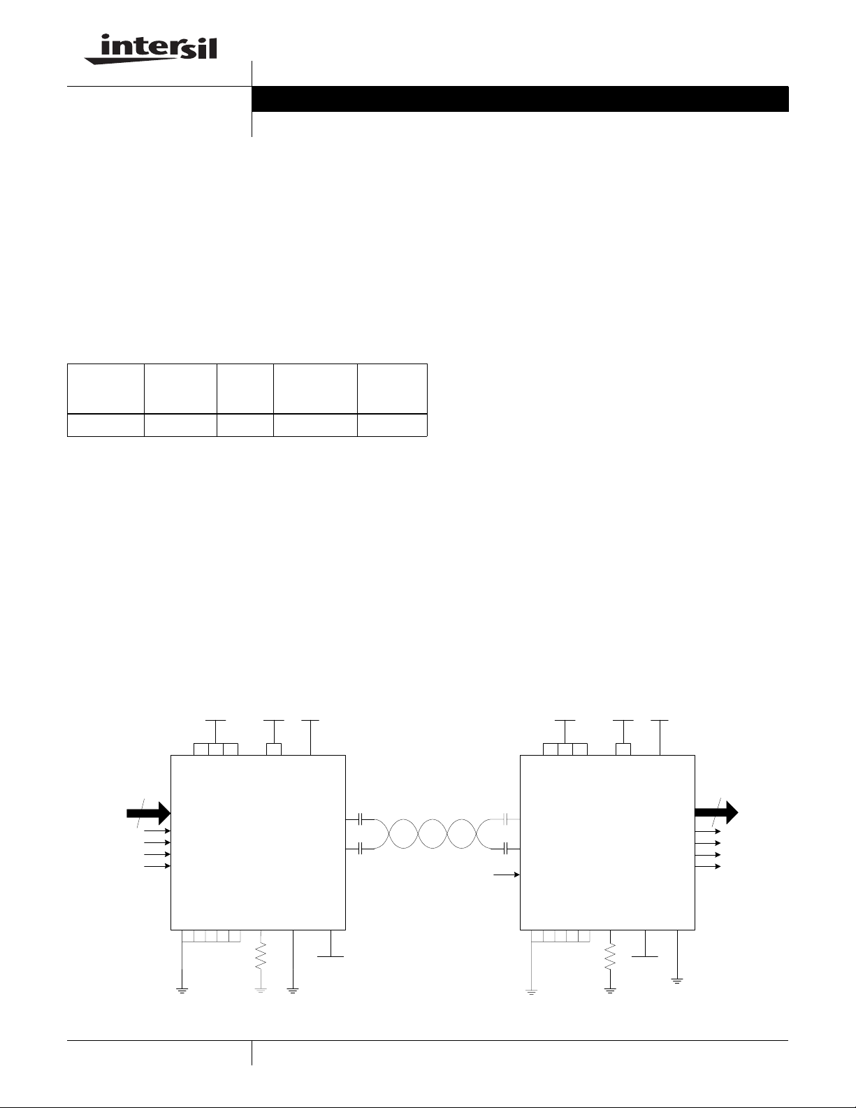
VIDEO
SOURCE
• Video entertainment systems
• Industrial computing terminals
• Remote cameras
3.3V 1.8V VDD_IO 3.3V 1.8V VDD_IO
VDD_TX
RGBA/B/C
VSYNC
HSYNC
DATAEN
PCLK_IN
GND_CR
GND_AN
VDD_AN
GND_P
GND_TX
24 24
VDD_CR
VDD_CDR
RSTB/PDB
SERIOP
ISL34340 ISL34340
REF_RES
GND_CDR
GND_IO
3.16 KΩ
I2CA0
SERION
VIDEO_TX
VDD_IO
10m DIFFERENTIAL CABLE
27nF
27nF
27nF
27nF
REF_CLK
VDD_TX
SERIOP
SERION
PCLK_IN
GND_CR
GND_AN
VDD_P
VDD_IO
VDD_AN
GND_P
GND_TX
VDD_P
VDD_IO
GND_CDR
GND_IO
VDD_CR
VDD_CDR
RSTB/PDB
RGBA/B/C
VSYNC
HSYNC
DATAEN
PCLK_OUT
VIDEO_TX
I2CA0
REF_RES
VDD_IO
3.16 KΩ
VIDEO
SINK
1
CAUTION: These devices are sensitive to electrostatic discharge; follow proper IC Handling Procedures.
1-888-INTERSIL or 1-888-468-3774
| Intersil (and design) is a registered trademark of Intersil Americas Inc.
All other trademarks mentioned are the property of their respective owners.
Copyright Intersil Americas Inc. 2008. All Rights Reserved
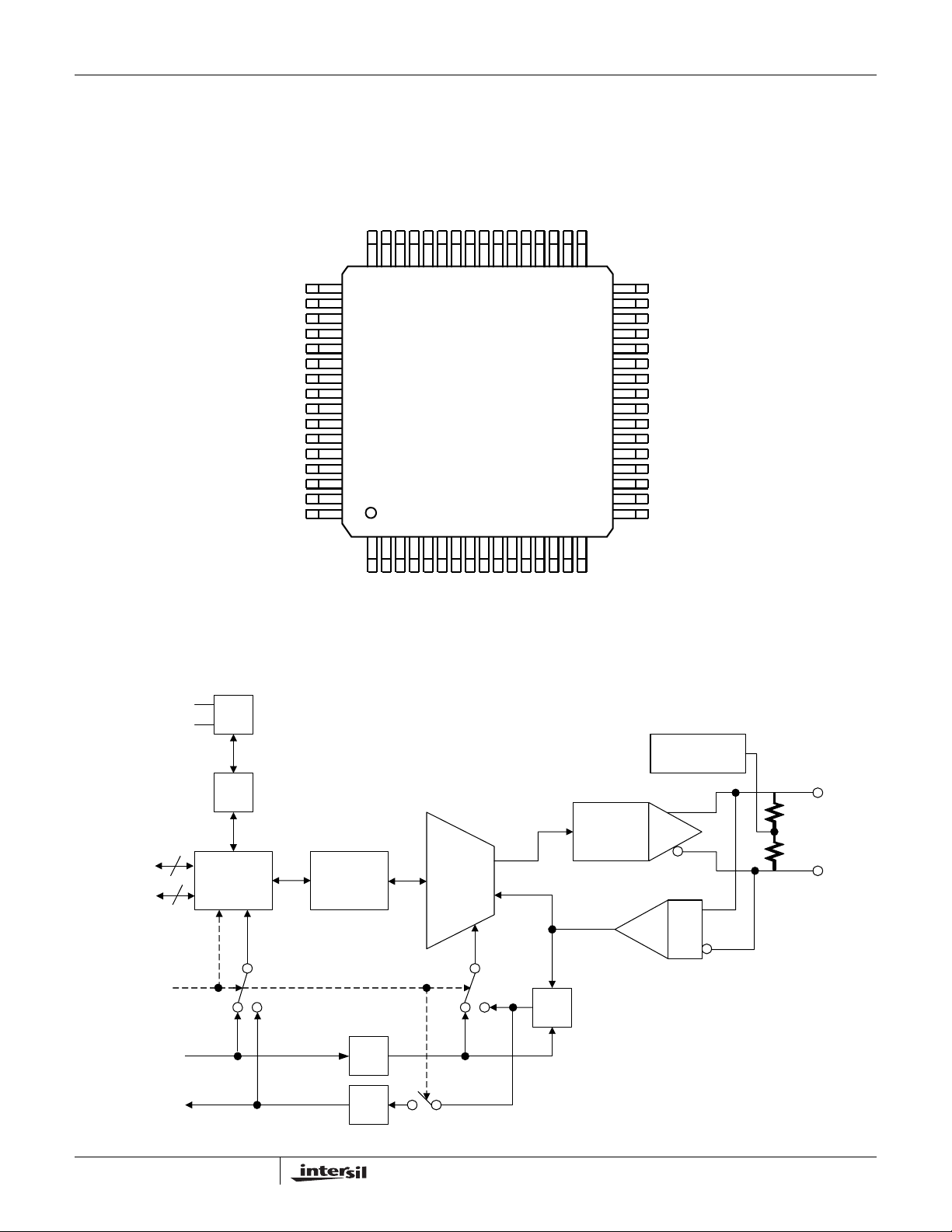
Pinout
www.BDTIC.com/Intersil
VDD_CDR
GND_IO
VDD_CDR
ISL34340
ISL34340
(64 LD EPTQFP)
TOP VIEW
SERIOP
GND_TX
VDD_TX
GND_CDR
GND_CDR
GND_TX
SERION
REF_RES
GND_AN
VDD_AN
TEST
I2CA1
I2CA0
Block Diagram
SCL
SDA
VIDEO_TX
VDD_IO
PCLK_OUT
GND_IO
I2C
RGBA0
RGBA1
RGBA2
RGBA3
RGBA4
RGBA5
RGBA6
RGBA7
RGBB0
RGBB1
RGBB2
RGBB3
484746454443424140393837363534
49
50
51
52
53
54
55
56
57
58
59
60
61
62
63
64
123456789101112131415
RGBC5
RGBC4
RGBC3
RGBC2
RGBC1
RGBC0
RGBB7
RGBB6
RGBB5
RGBB4
VDD_IO
RGBC7
RGBC6
16
STATUS
TEST_EN
RSTB/PDB
33
32
31
30
29
28
27
26
25
24
23
22
21
20
19
18
17
I2CA2
I2CA3
SDA
SCL
VDD_P
GND_P
PCLK_IN
VSYNCPOL
HSYNCPOL
VSYNC
HSYNC
DATAEN
VDD_CR
VDD_CR
GND_CR
GND_CR
VCM
GENERATOR
RAM
EMPHASIS
CDR
V/H/DE
RGB
24
VIDEO_TX
(HI)
PCLK_IN
(REF_CLK WHEN
VIDEO_TX IS LO)
PCLK_OUT
3
TDM
8b/10b
x30
÷30
MUX
DEMUX
2
PRE-
RX
TX
EQ
SERIOP
SERION
FN6255.1
June 23, 2008
ISL34340
www.BDTIC.com/Intersil
Absolute Maximum Ratings Thermal Information
Supply Voltage
VDD_P to GND_P, VDD_TX to GND_TX,
VDD_IO to GND_IO . . . . . . . . . . . . . . . . . . . . . . . -0.5V to 4.6V
VDD_CDR to GND_CDR, VDD_CR to GND_CR . . -0 .5V to 2.5V
Between any pair of GND_P, GND_TX,
GND_IO, GND_CDR, GND_CR . . . . . . . . . . . . . -0.1V to 0.1V
3.3V Tolerant LVTTL/LVCMOS Input Voltage
. . . . . . . . . . . . . . . . . . . . . . . . . . . . . . . . .-0.3V to VDD_IO + 0.3V
Differential Input Voltage . . . . . . . . . . . . . . .-0.3V to VDD_IO + 0.3V
Differential Output Current . . . . . . . . . . . . . .Short Circuit Protected
LVTTL/LVCMOS Outputs. . . . . . . . . . . . . . . .Short Circuit Protected
ESD Rating
Human Body Model
All pins . . . . . . . . . . . . . . . . . . . . . . . . . . . . . . . . . . . . . . . . .4kV
SERIOP/N (all VDD Connected, all GND Connected) . . . . .8kV
Machine Model. . . . . . . . . . . . . . . . . . . . . . . . . . . . . . . . . . . .200V
CAUTION: Do not operate at or near the maximum ratings listed for extended periods of time. Exposure to such conditions may adversely impact product reliability and
result in failures not covered by warranty.
NOTES:
is measured in free air with the component mounted on a high effective thermal conductivity test board with “direct attach” features. See
1. θ
JA
Tech Brief TB379.
2. For θ
, the “case temp” location is the center of the exposed metal pad on the package underside.
JC
Thermal Resistance (Typical, Notes 1, 2) θ
EPTQFP. . . . . . . . . . . . . . . . . . . . . . . . 33 4.5
Maximum Power Dissipation. . . . . . . . . . . . . . . . . . . . . . . . . . . . 327mW
Maximum Junction Temperature . . . . . . . . . . . . . . . . . . . . . .+125°C
Maximum Storage Temperature Range. . . . . . . . . .-65°C to +150°C
Operating Temperature Range . . . . . . . . . . . . . . . . .-40°C to +85°C
Pb-free reflow profile . . . . . . . . . . . . . . . . . . . . . . . . . .see link below
http://www.intersil.com/pbfree/Pb-FreeReflow.asp
θJC (°C/W)
JA
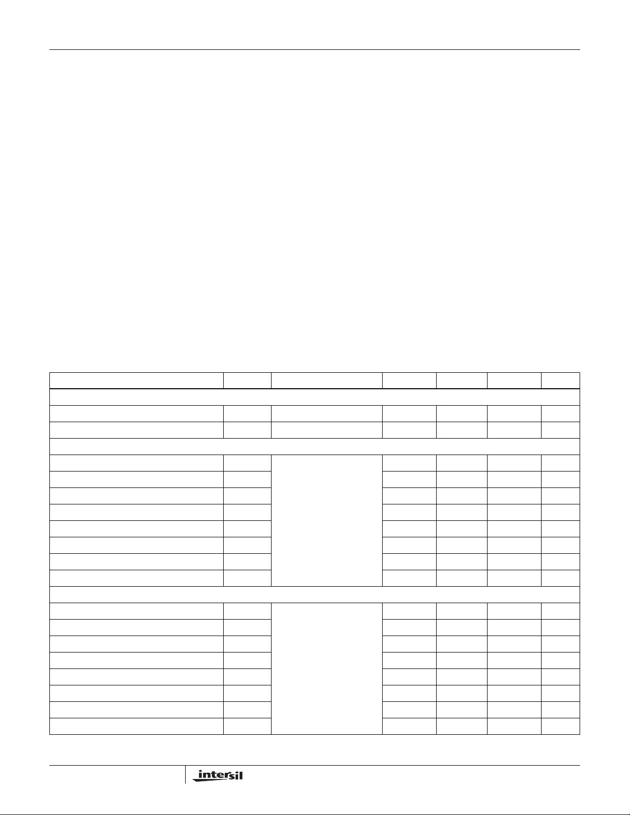
Electrical Specifications Unless otherwise indicated, all data is for: VDD_CDR
VDD_TX = VDD_P = VDD_AN = 3.3V, TA = +25°C, Ref_Res = 3.16kΩ, High-speed AC-coupling
capacitor = 27nF.
PARAMETER SYMBOL CONDITIONS MIN TYP MAX UNITS
POWER SUPPLY VOLTAGE
VDD_CDR, VDD_CR 1.7 1.8 1.9 V
VDD_TX, VDD_P, VDD_AN, VDD_IO 3.0 3.3 3.6 V
SERIALIZER POWER SUPPLY CURRENTS
Analog TX Supply Current I
Analog CDR Supply Current I
Digital I/O Supply Current I
Digital Supply Current I
PLL/VCO Supply Current I
Analog Bias Supply Current I
Total 1.8V Supply Current 77 90 mA
Total 3.3V Supply Current 40 46 mA
DESERIALIZER POWER SUPPLY CURRENTS
Analog TX Supply Current I
Analog CDR Supply Current I
Digital I/O Supply Current I
Digital Supply Current I
PLL/VCO Supply Current I
Analog Bias Supply Current I
Total 1.8V Supply Current 77 90 mA
Total 3.3V Supply Current 64 80 mA
DDTX
DDCDR
DDIO
DDCR
DDP
DDAN
DDTX
DDCDR
DDIO
DDCR
DDP
DDAN
VIDEO_TX = 1
PCLK_IN = 40MHz
VIDEO_TX = 0
REF_CLK = 40MHz
= VDD_CR = 1.8V, VDD_IO = 3.3V
17 mA
57 mA
12mA
20 mA
17 mA
5.5 mA
24 mA
45 mA
17 25 mA
32 mA
17 mA
5.4 mA
,
3
FN6255.1
June 23, 2008

ISL34340
www.BDTIC.com/Intersil
Electrical Specifications Unless otherwise indicated, all data is for: VDD_CDR
VDD_TX = VDD_P = VDD_AN = 3.3V, TA = +25°C, Ref_Res = 3.16kΩ, High-speed AC-coupling
capacitor = 27nF. (Continued)
PARAMETER SYMBOL CONDITIONS MIN TYP MAX UNITS
POWER-DOWN SUPPLY CURRENT
Total 1.8V Power-Down Supply Current RSTB = GND;
Total 3.3V Power-Down Supply Current 1mA
PARALLEL INTERFACE
High Level Input Voltage V
Low Level Input Voltage V
Input Leakage Current I
High Level Output Voltage V
Low Level Output Voltage V
Output Short Circuit Current I
Output Rise and Fall Times t
SERIALIZER PARALLEL INTERFACE
PCLK_IN Frequency f
PCLK_IN Duty Cycle t
Parallel Input Setup Time t
Parallel Input Hold Time t
DESERIALIZER PARALLEL INTERFACE
PCLK_OUT Frequency f
PCLK_OUT Duty Cycle t
PCLK_OUT Period Jitter (RMS) t
PCLK_OUT Spread Width t
Time to Parallel Output Data Valid t
Deserializer Output Latency t
DESERIALIZER REFERENCE CLOCK (REF_CLK IS FED INTO PCLK_IN)
REF_CLK Lock Time t
REF_CLK to PCLK_OUT Clock Maximum
Frequency Offset
HIGH-SPEED TRANSMITTER
HS Differential Output Voltage, Transition Bit VOD
HS Differential Output Voltage, Non-T ransition
Bit
OSC
OR/tOF
IDC
OUT
ODC
OSPRD
CPD
PLL
VOD
spec is per device
IH
IL
IN
I
OH
OL
IN
IS
IH
OJ
DV
TR
NTR
= -2.0mA, VDD_IO = 3V 0.8*VDD_IO V
OH
I
= 2.0mA, VDD_IO = 3V 0.2*VDD_IO V
OL
Slew rate control set to min,
= 8pF
C
L
Slew rate control set to max,
= 8pF
C
L
Clock randomizer off 0.5 %t
Clock randomizer on ±20 %t
Relative to PCLK_OUT -4.7 5.5 ns
Part-to-part,
side-channel disabled
PCLK_OUT is the
recovered clock
TXCN = 0x00 600 825 990 mV
TXCN = 0x0F 1170 mV
TXCN = 0xF0 975 mV
TXCN = 0xFF 1300 mV
TXCN = 0x00 600 825 990 mV
TXCN = 0x0F 460 mV
TXCN = 0xF0 975 mV
TXCN = 0xFF 600 mV
= VDD_CR = 1.8V, VDD_IO = 3.3V
0.5 mA
2.0 V
-10 ±0.01 10 µA
1ns
4ns
640MHz
40 50 60 %
3.6 ns
1.6 ns
640MHz
50 %
4 9 14 PCLK
100 µs
1500 5000 ppm
,
0.8 V
50 mA
PCLK
PCLK
P-P
P-P
P-P
P-P
P-P
P-P
P-P
P-P
4
FN6255.1
June 23, 2008

ISL34340
www.BDTIC.com/Intersil
Electrical Specifications Unless otherwise indicated, all data is for: VDD_CDR
VDD_TX = VDD_P = VDD_AN = 3.3V, TA = +25°C, Ref_Res = 3.16kΩ, High-speed AC-coupling
capacitor = 27nF. (Continued)
PARAMETER SYMBOL CONDITIONS MIN TYP MAX UNITS
HS Generated Output Common Mode Voltage V
HS Common Mode Serializer-Deserializer
Voltage Difference
HS Differential Output Impedance R
HS Output Latency t
HS Output Rise and Fall Times t
HS Differential Skew t
HS Output Random Jitter t
HS Output Deterministic Jitter t
HIGH SPEED RECEIVER
HS Differential Input Voltage V
HS Generated Input Common Mode Voltage V
HS Differential Input Impedance R
HS Maximum Jitter Tolerance 0.52 UI
I2C
2
C Clock Rate (on SCL) f
I
I2C Clock Pulse Width (HI or LO) 1.3 µs
2
C Clock Low to Data Out Valid 0 1 µs
I
2
C Start/Stop Setup/Hold Time 0.6 µs
I
I2C Data in Setup Time 100 ns
2
C Data in Hold Time 100 ns
I
2
C Data out Hold Time 100 ms
I
OCM
ΔV
CM
OUT
LPD
R/tF
SKEW
RJ
DJ
ID
ICM
IN
I2C
Part-to-part 4 7 10 PCLK
20% to 80% 150 ps
= VDD_CR = 1.8V, VDD_IO = 3.3V
2.35 V
20 120 mV
80 100 120 Ω
<10 ps
13.4 ps
40 ps
150 mV
2.32 V
80 100 120 Ω
100 400 kHz
,
RMS
P-P
P-P
P-P
Pin Descriptions
DESCRIPTION
PIN NUMBER PIN NAME
52 to 63,
2 to 13
22 HSYNC Horizontal (line) Sync LVCMOS input Horizontal (line) Sync LVCMOS output
23 VSYNC Vertical (frame) Sync LVCMOS input Vertical (frame) Sync LVCMOS output
21 DATAEN Video Data Enable LVCMOS input Video Data Enable LVCMOS output
26 PCLK_IN Pixel clock LVCMOS input PLL reference clock LVCMOS input
51 PCLK_OUT Default; not used Recovered clock LVCMOS output
41, 40 SERIOP, SERION High speed differential serial I/O High speed differential serial I/O
24 HSYNCPOL CMOS input for HSYNC
25 VSYNCPOL CMOS input for VSYNC
RGBA[7:0],
RGBB[7:0], RGBC[7:0]
Parallel video data LVCMOS inputs Parallel video data LVCMOS outputs
1: HSYNC is active low
0: HSYNC is active high
1: VSYNC is active low
0: VSYNC is active high
5
SERIALIZER DESERIALIZER
FN6255.1
June 23, 2008

ISL34340
www.BDTIC.com/Intersil
Pin Descriptions (Continued)
DESCRIPTION
PIN NUMBER PIN NAME
49 VIDEO_TX CMOS input for video flow direction
1: video serializer
0: video deserializer
2
29, 30 SDA, SCL I
31 to 34 I2CA[3:0] I
16 RSTB/PDB CMOS input for Reset and Power-down. For normal operation, this pin must be forced high. When
14 STATUS CMOS output for Receiver Status:
36 REF_RES Analog bias setting resistor connection; use 3.16kΩ ±1% to ground
27 GND_P PLL Ground
48, 64 GND_IO Digital (Parallel and Control) Ground
44, 45 GND_CDR Analog (Serial) Data Recovery Ground
39, 42 GND_TX Analog (Serial) Output Ground
37 GND_AN Analog Bias Ground
17, 18 GND_CR Core Logic Ground
19, 20 VDD_CR Core Logic VDD
43 VDD_TX Analog (Serial) Output VDD
38 VDD_AN Analog Bias VDD
46, 47 VDD_CDR Analog (Serial) Data Recovery VDD
1, 50 VDD_IO Digital (Parallel and Control) VDD
28 VDD_P PLL VDD
15, 35 TEST_EN, TEST Must be connected to ground
Exposed Pad Exposed Pad Must be connected to ground
NOTES:
3. Pins with the same name are internally connected together. However, this connection must NOT be used for connecting together external
components or features.
4. The various differently-named Ground pins are internally weakly connected. They must be tied together externally. The different names are
provided to assist in minimizing the current loops involved in bypassing the associated supply VDD pins. In particular, for ESD testing, they
should be considered a common connection.
C Interface Pins (I2C DATA, I2C CLK)
2
C Device Address
this pin is forced low, the device will be reset. If this pin stays low, the device will be in PD mode.
1: Valid 8b/10b data received
0: otherwise
Note: serializer and deserializer switch roles during side-channel reverse traffic
SERIALIZER DESERIALIZER
6
FN6255.1
June 23, 2008

Diagrams
www.BDTIC.com/Intersil
VOD
ISL34340
TR
VOD
NTR
TXCN
0x00
0x0F
0xF0
0xFF
FIGURE 1. VOD vs TXCN SETTING
VIDEO_TX = 1
PCLK_IN
RGB[A:C][7:0]
HSYNC
VSYNC
DATAEN
FIGURE 2. PARALLEL VIDEO INPUT TIMING [HSYNCPOL = 0, VSYNCPOL = 0, PCLKPOL (reg) = 0]
1/f
IN
T
IS
VALID DATA VALID DATA DATA IGNORED DATA IGNORED VALID DATA
T
IH
T
IS
T
IDC
T
IH
7
FN6255.1
June 23, 2008

ISL34340
www.BDTIC.com/Intersil
VIDEO_TX = 0
PCLK_OUT
RGB[A:C][7:0]
HSYNC
VSYNC
DATAEN
T
DV
FIGURE 3. PARALLEL VIDEO OUTPUT TIMING [HSYNCPOL = 0, VSYNCPOL = 0, PCLKPOL (reg) = 0]
1/f
OUT
VALID DATA VALID DATA DATA HELD AT PREVIOUS VALUE VALID DATA
Applications
Overview
A pair of ISL34340 SERDES transports 24-bit parallel video
(16-bit parallel video for the ISL34320) along with auxiliary
data over a single 100Ω differential cable either to a display
or from a camera. Auxiliary data is transferred in both
directions and can be used for remote configuration and
telemetry.
The benefits include lower EMI, lower costs, greater
reliability and space savings. The same device can be
configured to be either a serializer or deserializer by setting
one pin (VIDEO_TX), simplifying inventory. RGBA/B/C,
VSYNC, HSYNC, and DATAEN pins are inputs in serializer
mode and outputs in deserializer mode.
The video data presented to the serializer on the parallel
LVCMOS bus is serialized into a high-speed differential
signal. This differential signal is converted back to parallel
video at the remote end by the deserializer. The
side-channel data is transferred between the SERDES pair
during two lines of the vertical video blanking interval.
When the side-channel is enabled, there will be a number of
PCLK cycles uncertainty from frame-to-frame. This should
not cause sync problems with most displays, as this occurs
during the vertical front porch of the blanking period. When
properly configured, the SERDES link supports end-to-end
transport with fewer than one error in 10
10
bits.
T
OR
T
DV
T
OF
T
ODC
PCB traces need to be adjacent and matched in length (so
as to minimize the imbalanced coupling to other traces or
elements), and of a geometry to match the impedance of the
transmitter and receiver, to minimize reflections. Similar care
needs to be applied to the choice of connectors and cables.
SERIOP and SERION pins incorporate internal differential
termination of the serial signal lines. External termination
cannot be used unless the side-channel is disabled.
SERIO Pin AC-Coupling
AC-coupling minimizes the effects of DC common mode
voltage difference and local power supply variations
between two SERDES. The serializer outputs DC balanced
8b/10b line code, which allows AC-coupling.
The AC-coupling capacitor on SERIO pins must be 27nF on
the serializer board and 27nF on the deserializer board. The
value of the AC-coupling capacitor is very critical since a
value too small will attenuate the high speed signal at low
clock rate. A value too big will slow down the turn around
time for the side-channel.
Receiver Reference Clock (REF_CLK)
The reference clock (REF_CLK) for the PLL is fed into
PCLK_IN pin. REF_CLK is used to recover the clock from
the high speed serial stream. REF_CLK is very sensitive to
any instability. The following conditions must be met at all
times after power is applied to the deserializer, or else the
deserializer may need a manual reset:
Differential Signals and T ermination
The ISL34340 serializes the 24-bit parallel data at 30x the
PCLK_IN frequency. The ISL34320 serializes the 16-bit
parallel data at 20x the PCLK_IN frequency. The extra 2 bits
per word come from the 8b/10b encoding scheme.
The high bit rate of the differential serial data requires
special care in the layout of traces on PCBs, in the choice
and assembly of connectors, and in the cables themselves.
• REF_CLK frequency must be within the limits specified
• REF_CLK amplitude must be stable.
A simple 3.3V CMOS crystal oscillator can be used for
REF_CLK.
Power Supply Sequencing
The 3.3V supply must be higher than the 1.8V supply at all
times, including during power-up and power-down. To meet
8
FN6255.1
June 23, 2008

ISL34340
www.BDTIC.com/Intersil
this requirement, the 3.3V supply must be powered up
before the 1.8V supply.
For the deserializer, REF_CLK must not be applied before
the device is fully powered up. Applying REF_CLK before
power-up may require the deserializer to be manually reset.
A 10ms delay after the 1.8V supply is powered up
guarantees normal operation.
Power Supply Bypassing
The serializer and deserializer functions rely on the stable
functioning of PLLs locked to local reference sources or
locked to an incoming signal. It is important that the various
supplies (VDD_P, VDD_AN, VDD_CDR, VDD_TX) be well
bypassed over a wide range of frequencies, from below the
typical loop bandwidth of the PLL to approaching the signal
bit rate of the serial data. A combination of different values of
capacitors from 1000pF to 5µF or more with low ESR
characteristics is generally required.
The parallel LVCMOS VDD_IO
sensitive, but since the RGB and SYNC/DATAEN signals
can all swing on the same clock edge, the current in these
pins and the corresponding GND pins can undergo
substantial current flow changes, so once again, a
combination of different values of capacitors over a wide
range, with low ESR characteristics, is desirable.
supply is inherently less
Capacitors of 0.1µF offer low impedance in the 10MHz to
20MHz region, and 1000pF capacitors in the 100MHz to
200MHz region. In general, one of the lower value capacitors
should be used at each supply pin on the IC. Figure 4 shows
the grounding of the various capacitors to the pin
corresponding to the supply pin. Although all the ground
supplies are tied together, the PCB layout should be
arranged to emulate this arrangement, at least for the
smaller value (high frequency) capacitors, as much as
possible.
A set of arrangements of this type is shown in Figure 4,
where each supply is bypassed with a ferrite-bead-based
choke, and a range of capacitors. A “choke” is preferable to
an “inductor” in this application, since a high-Q inductor will
be likely to cause one or more resonances with the shunt
capacitors, potentially causing problems at or near those
frequencies, while a “lossy” choke will reflect a high
impedance over a wide frequency range.
The higher value capacitor, in particular, needs to be chosen
carefully, with special care regarding its ESR. Very good
results can be obtained with multilayer ceramic capacitors,
available from many suppliers, and generally in small
outlines (such as the 1210 outline suggested in the
schematic shown in Figure 4), which provide good bypass
capabilities down to a few mΩ at 1MHz to 2MHz. Other
capacitor technologies may also be suitable (perhaps
niobium oxide), but “classic” electrolytic capacitors
frequently have ESR values of above 1Ω, that nullify any
decoupling effect above the 1kHz to 10kHz frequency range.
All Intersil U.S. products are manufactured, assembled and tested utilizing ISO9000 quality systems.
Intersil Corporation’s quality certifications can be viewed at www.intersil.com/design/quality
Intersil products are sold by description only. Intersil Corporation reserves the right to make changes in circuit design, software and/or specifications at any time without
notice. Accordingly, the reader is cautioned to verify that data sheets are current before placing orders. Information furnished by Intersil is believed to be accurate and
reliable. However, no responsibility is assumed by Intersil or its subsidiaries for its use; nor for any infringements of patents or other rights of third parties which may result
from its use. No license is granted by implic atio n or other wise u nde r any p a tent or patent rights of Intersil or it s sub sidi ari es.
For information regarding Intersil Corporation and its products, see www.intersil.com
I2C Interface
The I2C interface allows access to internal registers used to
configure the SERDES and to obtain status information. A
serializer must be assigned a different address than its
deserializer counterpart. The upper 3 bits are permanently
set to 011 and the lower 4 bits determined by pins as follows:
0 1 1 I2CA3 I2CA2 I2CA1 I2CA0 R/W
Thus, 16 SERDES can reside on the same bus. By
convention, when all address pins are tied low, the device
address is referred to as 0x60.
SCL and SDA are open drain to allow multiple devices to
share the bus. If not used, SCL and SDA should be tied to
VDD_IO.
FIGURE 4. POWER SUPPLY BYPASSING
9
FN6255.1
June 23, 2008

ISL34340
www.BDTIC.com/Intersil
Thin Plastic Quad Flatpack Exposed Pad Plastic Packages (EPTQFP)
D
D1
-D-
Q64.10x10B (JEDEC MS-026ACD-HU ISSUE D)
64 LEAD THIN PLASTIC QUAD FLATPACK EXPOSED
PAD PACKAGE
MILLIMETERS
-A-
EJECTOR PIN MARK
NOT PIN #1 ID
-B-
SYMBOL
A-1.20-
A1 0.05 0.15 -
A2 0.95 1.05 -
NOTESMIN MAX
b 0.16 0.28 6
b1 0.17 0.23 -
E1
E
D 11.80 12.20 3
D1 9.90 10.10 4, 5
D2 3.46 3.76 -
e
E 11.80 12.20 3
E1 9.90 10.10 4, 5
E2 3.46 3.76 -
L 0.45 0.75 -
N647
PIN 1
TOP VIEW
e 0.50 BSC -
Rev. 2 4/08
GAGE
PLANE
0o-7
o
0.020
MIN
0.008
0o MIN
o
L
0.25
0.010
11o-13
11o-13
A2
A1
o
NOTES:
1. Controlling dimension: MILLIMETER. Converted inch
dimensions are not necessarily exact.
2. All dimensions and tolerances per ANSI Y14.5M-1982.
3. Dimensions D and E to be determined at seating plane .
-C-
4. Dimensions D1 and E1 to be determined at datum plane
-H-
.
5. Dimensions D1 and E1 do not include mold protrusion.
Allowable protrusion is 0.25mm (0.010 inch) per side.
6. Dimension b does not include dambar protrusion. Allowable
dambar protrusion shall not cause the lead width to exceed
PIN 1
the maximum b dimension by more than 0.08mm (0.003
inch).
7. “N” is the number of terminal positions.
EJECTOR PIN MARK
NOT PIN #1 ID
-H-
E2
EJECTOR PIN MARK
NOT PIN #1 ID
D2
BOTTOM VIEW
10
0.08
0.003
0.09/0.16
0.004/0.006
BASE METAL
WITH PLATING
SEATING
PLANE
A
-C-
D
A-B S
SCM
b
b1
0.09/0.20
0.004/0.008
FN6255.1
June 23, 2008
0.08
0.003
 Loading...