

Page 1
®
ISL29002
Data Sheet December 1, 2006
Light-to-Digital I2C Sensor
The ISL29002 is an integrated light sensor with a built-i n
integrating type ADC and a standard I2C interface. The
device transforms illuminance, ambient light level in lux, into
a digital output signal accessible through I
2
C. The sensor
precisely converts illuminance from 1lux to 100,000lux. The
ADC features up to 15-bit effective resolution. The sensor
includes another photodiode covered with metal to reduce
the effects of dark output reading that may be significant in
low lux levels.
The ISL29002 can control display panel backlighting depending
on ambient light conditions, adding artificial intelligence by
approximating the response of a human eye. The ISL29002
can also manage portable peripheral illumination based upon
lighting conditions extending battery life.
In normal operation, the ISL29002 consumes less than 300µA
of supply current. A software power down mode is controlled
2
via the I
C interface and disables all but the I2C interface. The
supply current is then reduced to less than 88µA.
Designed to operate on supplies from 2.5V to 3.3V, the
ISL29002 is specified for operation over the -40°C to +85°C
ambient temperature range. It is packaged in a clear, Pb-free
8 Ld ODFN package.
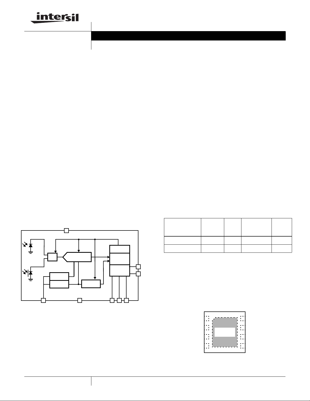
Block Diagram
VDD
1
PHOTODIODE 1
COMMAND
REGISTER
MUX
PHOTODIODE2
IREF
FOSC
INTEGRATING
ADC
COUNTER
16
2
DATA
REGISTER
2
C
I
7
8
SCL
SDA
FN7465.2
Features
•I2C interface fast mode at 400kHz
• 88µA disabled current
• Adjustable max lux range: 10,000lux to 100,000lux
• Up to 15-bit effective resolution
• Adjustable resolution: 0.15 to 1.65 counts per lux
• Simple output code proportional to lux
• Flicker/noise rejection
• Variable integration time; 50ms to 550ms
• 2.5V to 3.3V supply
• 8 Ld ODFN (3mmx3mm)
• Temperature compensation
• Pb-free available (RoHS compliant)
Applications
• Backlight sensing
• Automatic backlight adjustment
• Backlight linearity adjustments
Ordering Information
TEMP.
PART NUMBER
(Note)
ISL29002IROZ -40 to +85 - 8 Ld 3x3 ODFN MDP0052
ISL29002IROZ-T7 -40 to +85 7” 8 Ld 3x3 ODFN MDP0052
NOTE: Intersil Pb-free ODFN products employ special Pb-free material
sets; molding compounds/die attach materials and 100% matte tin plate
termination finish, which are RoHS compliant and compatible with both
SnPb and Pb-free soldering operations. Intersil Pb-free products are
MSL classified at Pb-free peak reflow temperatures that meet or exceed
the Pb-free requirements of IPC/JEDEC J STD-020.
RANGE
(°C)
TAPE &
REEL
PACKAGE
(Pb-Free)
PKG.
DWG. #
3 2 6 5 4
R
EXT
GND A1A2 A0
1
Pinout
VDD
GND
R
EXT
A0
CAUTION: These devices are sensitive to electrostatic discharge; follow proper IC Handling Procedures.
1-888-INTERSIL or 1-888-468-3774
| Intersil (and design) is a registered trademark of Intersil Americas Inc.
All other trademarks mentioned are the property of their respective owners.
Copyright © Intersil Americas Inc. 2006. All Rights Reserved.
ISL29002
(8 LD ODFN)
TOP VIEW
1
2
THERMAL
3
4
PAD
8
SDA
SCL
7
A2
6
A1
5
Page 2
ISL29002
Absolute Maximum Ratings (T
Maximum Supply Voltage between V
2
I
C Address Pin Voltage (A2, A1, A0) . . . . . . . . . . . . . -0.2V to 3.6V
2
I
C Bus Pin Voltage (SCL, SDA). . . . . . . . . . . . . . . . . -0.2V to 5.5V
2
I
C Bus Pin Current (SCL, SDA) . . . . . . . . . . . . . . . . . . . . . . <10mA
R
Pin Voltage. . . . . . . . . . . . . . . . . . . . . . . . . . . . . -0.2V to 3.6V
EXT
Operating Temperature . . . . . . . . . . . . . . . . . . . . . . .-40°C to +85°C
CAUTION: Stresses above those listed in “Absolute Maximum Ratings” may cause permanent damage to the device. This is a stress only rating and operation of the
device at these or any other conditions above those indicated in the operational sections of this specification is not implied.
IMPORTANT NOTE: All parameters having Min/Max specifications are guaranteed. Typical values are for information purposes only. Unless otherwise noted, all tests
are at the specified temperature and are pulsed tests, therefore: TJ = TC = T
Electrical Specifications V
= +25°C)
A
and GND . . . . . . . . . . 3.6V
DD
= 3V, TA = +25°C, R
DD
Maximum Die Temperature . . . . . . . . . . . . . . . . . . . . . . . . . . +125°C
Storage Temperature. . . . . . . . . . . . . . . . . . . . . . . .-45°C to +100°C
ESD, Human Body Model . . . . . . . . . . . . . . . . . . . . . . . . . . . . . .2kV
A
= 100kΩ 1%, I2C command = 00(hex) (Note 1), unless otherwise specified.
EXT
PARAMETER DESCRIPTION CONDITION MIN TYP MAX UNIT
V
DD
I
DD
I
DD1
t
UPD
f
OSC
F
I2C
DATA0 Dark ADC Code E = 0lux
Power Supply Range 2.25 3.63 V
Supply Current 0.3 0.375 mA
Supply Current Software disabled 88 110 µA
Internal Update Time/Conversion Time 85 110 135 ms
Internal Oscillator Frequency 300 kHz
I2C Clock Rate (Note 2) 1 400 kHz
1 Counts
E = 0lux, integration time = 550ms 4
DATA1 ADC Code ADC full scale count value 32,768 Counts
DATA2 ADC Code E = 25,000lux, Fluorescent light
13,500 16,000 18,500 Counts
(Note 3)
V
V
V
I
SDA
I
IL
I
IH
REF
TL
TH
Voltage of R
SCL, SDA, A0, A1, and A2 Threshold LO (Note 4) 1.05 V
SCL, SDA, A0, A1, and A2 Threshold HI (Note 4) 1.95 V
SDA Current Sinking Capability 3 5 mA
A0, A1, and A2 Input Current LO A0 = A1 = A2 = GND 0.1 µA
A0, A1, and A2 Input Current HI A0 = A1 = A2 = V
Pin 0.45 0.51 0.53 V
EXT
DD
0.1 µA
NOTES:
2
1. For I
2. Minimum I
C command = 00H, the ADC converts the current of (photo) diode 1 into a 16 bit data with an internally timed integration of 110ms for
R
= 100kΩ, 1% tolerance.
EXT
2
C Clock Rate is guaranteed by design.
3. Fluorescent light is substituted by an LED at production.
4. The voltage threshold levels of the SDA and SCL pins are VDD dependent: V
= 0.35*VDD. VTH = 0.65*VDD.
TL
2
FN7465.2
December 1, 2006
Page 3
ISL29002
Pin Descriptions
PIN NUMBER PIN NAME DESCRIPTION
1 VDD Positive supply. Connect to a clean 2.25V to 3.3V supply
2 GND Ground. The thermal pad is connected to the GND pin
3R
EXT
4 A0 Bit 0 of the I
5 A1 Bit 1 of the I
6 A2 Bit 2 of the I
7SCLI
8SDAI
External resistor pin is for the ADC reference current, the integration time adjustment in internal timing
mode, and lux range/resolution adjustment. 100kΩ 1% tolerance resistor recommended.
2
C address. The address pins have an open gate equivalent circuit. These are the
2
C address.
2
C address.
2
C serial clock line The I2C bus lines can pulled above VDD, 5.5V max.
2
C serial data line
least-significant bits of the I
40(hex) through 48(hex).
2
C address. The eight possible addresses are
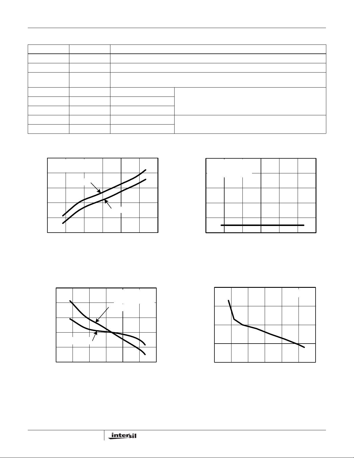
Typical Performance Curves R
320
TA = +27°C
Ta= 27oC
COMMAND = 00H
COMMAND = 00H
306
25000 lux
292
278
1000 lux
264
SUPPLY CURRENT (μA)
250
2.0 2.3 2.6 2.9 3.2 3.5 3.8
SUPPLY VOLTAGE (V)
EXT
= 100kΩ
10
TA = +27°C
Ta = 27oC
COMMAND = 00H
COMMAND = 00H
0 lux
8
0 lux
6
4
2
OUTPUT CODE (COUNTS)
0
2.0 2.3 2.6 2.9 3.2 3.5 3.8
SUPPLY VOLTAGE (V)
FIGURE 1. SUPPLY CURRENT vs SUPPLY VOLTAGE FIGURE 2. OUTPUT CODE FOR 0LUX vs SUPPLY VOLTAGE
1.015
1.010
Ta= 27oC
TA = +27°C
COMMAND = 00H
COMMAND = 00H
25000 lux
320.0
319.5
TA = +27°C
Ta = 27oC
1.005
319.0
1.000
(% FROM 3V)
0.995
OUTPUT CODE RATIO
0.990
2.0 2.3 2.6 2.9 3.2 3.5 3.8
1000 lux
SUPPLY VOLTAGE (V)
318.5
318.0
OSCILLATOR FREQUENCY (kHz)
2.0 2.3 2.6 2.9 3.2 3.5 3.8
SUPPLY VOLTAGE (V)
FIGURE 3. OUTPUT CODE vs SUPPLY VOLTAGE FIGURE 4. OSCILLATOR FREQUENCY vs SUPPLY VOLTAGE
3
December 1, 2006
FN7465.2
Page 4

ISL29002
Typical Performance Curves R
315
Vdd= 3V
COMMAND = 00H
305
295
285
275
SUPPLY CURRENT (μA)
265
25000 lux
1000 lux
-60 -20 20 60 100
TEMPERATURE (oC)
= 100kΩ (Continued)
EXT
10
Vdd = 3V
COMMAND = 00H
8
0 lux
6
4
2
OUTPUT CODE (COUNTS)
0
-60 -20 20 60 100
TEMPERATURE (oC)
FIGURE 5. SUPPLY CURRENT vs TEMPERATURE FIGURE 6. OUTPUT CODE FOR 0LUX vs TEMPERATURE
1.080
Vdd= 3V
330
COMMAND = 00H
1.048
25000 lux
329
Vdd = 3V
1.016
C)
o
0.984
(% FROM 25
0.952
1000 lux
OUTPUT CODE RATIO
0.920
-60 -20 20 60 100
TEMPERATURE (oC)
FIGURE 7. OUTPUT CODE vs TEMPERATURE
k = 7.5
100
n = 1.85
80
60
40
20
NORMALIZED RESPONSE (%)
0
300 400 500 600 700 800 900 1000 1100
HUMAN VISIBILITY CIE STANDARD
D1 NORMALIZED
n(D1-kD2)
NORMALIZED
D2
NORMALIZED
WAVELENGTH (nm)
FIGURE 9. RELATIVE INTENSITY FIGURE 10. RADIATION PATTERN
328
327
326
325
OSCILLATOR FREQUENCY (kHz)
-60 -20 20 60 100
TEMPERATURE (oC)
FIGURE 8. OSCILLATOR FREQUENCY vs TEMPERATURE
RADI ATI ON PATTERN
LUMINOSI T Y
ANGLE
RELATIVE SENSITIVITY
4
FN7465.2
December 1, 2006
Page 5

ISL29002
Principles of Operation
Photodiodes and ADC
The ISL29002 contains two photodiodes. One of the
photodiodes is sensitive to visible and infrared light (Diode 1).
Another photodiode (Diode 2) is covered with metal and can be
used to cancel the effects of dark output code, the unwanted
number of counts in the absence of light. Diode 2 can also be
used to cancel the presence of IR. See IR rejection in the
applications section. The ISL29002 also contains an on-chip
integrating analog-to-di git al co nvert er (ADC) to conve rt
photodiode currents into digital data. The interface to the ADC
is implemented using the standard I
The ISL29002’s built-in ADC is a charge-balancing
integrating converter type. The integrating ADC converts the
photodiode current to frequency. The repetition rate is then
counted by a binary counter to output a digital code - number
of counts. The ISL29002 can be configured (in external
timing mode) to output a maximum 2
The ADC has two timing controls, internal timing and
external timing. With internal timing, the number of clock
cycles per integration time is fixed at 2
number of counts is limited to 2
timing, the user have the flexibility to vary the maximum
number of counts up to 2
16
In addition, the ADC has three operating modes (Please
consult Table 1 for a complete list of modes.) In the first
operating mode, the ADC only integrates Diode 1's current. In
the second operating mode, the ADC only integrates the other
diode, Diode 2’s current. Both operating mode 1 and mode 2
has a 16-bit unsigned-magnitude format. In the third operating
mode, the ADC integrates Diode 2's current first, then Diode 1's
current. In this mode, the output is a 16-bit 2’s complem ent
format. The total integration time is doubled, and the digital
output is the difference of the two photodiode currents (Diode
1’s current minus Diode 2’s current). Any of the three operating
modes can be used with either of the two timing controls, either
internally or externally controlled integration timing.
I2C Interface
The ISL29002 contains a single 8-bit command register that
can be written via the I
defines the operation of the device, which does not change
until the command register is overwritten.
The ISL29002 contains four 8-bit data registers that can be
read via the I
2
C interface. The first two data registers contain
the ADC's latest digital output, while the second two
registers contain the number of clock cycles in the previous
integration period.
The ISL29002’s I
and A2. These pins can be tied or driven either high or low.
They comprise the least-significant three bits of the I
address, while the four most-significant bits are hardwired as
2
C interface. The command register
2
C address is pin-selectable by pins A0, A1,
2
C interface.
16
(65,536) counts.
15
15
(32,726), hence the
(32,7268). With external
(65,536).
2
C
1000. The eight possible addresses are therefore 40H through
47H.
Figure 11B shows a sample one-byte read. (A typical
application will read two to four bytes, however.) The I
2
C bus
master always drives the SCL (clock) line, while either the
master or the slave can drive the SDA (data) line. Every I
2
C
transaction begins with the master asserting a start condition
(SDA falling while SCL remains high). The following byte is
driven by the master, and includes the slave address and
read/write bit. The receiving device is responsible for pulling
SDA low during the acknowledgement period.
Any writes to the ISL29002 overwrite the command register,
changing the device’s mode. Any reads from the ISL29002
return two or four bytes of sensor data and counter value,
depending upon the operating mode. Neither the command
register nor the data registers have internal addresses, and
none of the registers can be individually addressed.
2
Every I
C transaction ends with the master asserting a stop
condition (SDA rising while SCL remains high).
I2C Transaction Flow
To WRITE, the master sends slave address 44(hex) plus the
write bit. Then master sends the ADC command to the
device which defines its operation. As soon as the ISL29002
receives the ADC command, it will execute and then store
the readings in the register after the analog-to-digital
conversion is complete. While the ISL29002 is executing the
command and also after the execution, the I
available for transactions other than the ISL29002. After
command execution, sensor data readings are stored in the
registers. Note that if a READ is received before the
execution is finished, the data retrieved is previous data
sensor reading. Typical integration/conversion time is 100ms
(for R
= 100k and internal timing mode). It is
EXT
recommended that a READ is sent 120ms later because the
fosc variation is 20%.
The operation of the device does not change until the
command register is overwritten. Hence, when the master
sends a slave address 44(hex) and a write bit, the ISL29002
will repeat the same command from the previous WRITE
transaction.
To READ, master sends slave address 44(hex) plus the read
bit. Then ISL29002 will hold the SDA line to send data to
master. Note that the master need not send an address register
to access the data. As soon as the ISL29002 receives the read
bit. It will send 4 bytes. The 1st byte is the LSB of the sensor
reading. The 2nd byte is the MSB of the sensor reading. The
3rd byte is LSB of the counter reading. The 4th byte is the MSB
of the counter reading. If internal timing mode is selected, only
the 1st and 2nd data byte are necessary; the master can assert
a stop after the 2nd data byte is received.
For more information about the I
the Philips® I
2
C specification documents.
2
C standard, please consult
2
C bus is
5
FN7465.2
December 1, 2006
Page 6

ISL29002
Command Register
The command register is used to define the ADC's
operations. Table 1 shows the primary commands used to
control the ADC.
Note that there are two classes of operat in g comma n ds :
three for internal timing, and three for external (arbitrary)
timing.
When using any of the three internal timing commands, the
device self-times each conversion, which is nominally 110ms
(with
R
= 100kΩ).
EXT
COMMAND FUNCTION
8C(hex) ADC is powered-down. To enable ADC from a powered-down state, send any command to the ISL29002.
0C(hex) ADC is reset. A reset restarts the counter value to zero and returns the clock cycle to zero.
00(hex) Internal Timing Mode. Integration
04(hex) ADC converts Diode 2’s current (I
time is 110ms per photodiode.
08(hex) ADC converts I
30(hex) External Timing Mode. Each external
34(hex) ADC converts Diode 2’s current (I
38(hex) ADC converts I
timing command sent to the device
ends one integration period and
begins another.
1xxx_xxxx
(binary)
TABLE 1. COMMAND REGISTERS AND FUNCTIONS
ADC converts Diode 1’s current (I
ADC converts Diode 1’s current (I
2
I
C communication test. The value written to the command register can be read
back via the I
When using any of the three external timing commands,
each command received by the device ends one conversion
and begins another. The integration time of the device is
thus the time between one I
2
C external timing command and
the next. The integration time can be between 1ms and
100ms. The external timing commands can be used to
synchronize the ADC’s integrating time to a PWM dimming
frequency in a backlight system in order to eliminate noise.
) into an unsigned-magnitude 16-bit data.
DIODE1
) into unsigned-magnitude 16-bit data.
DIODE2
DIODE1-IDIODE2
DIODE1-IDIODE2
2
C bus.
into 2’s-complement 16-bit data.
) into unsigned-magnitude 16-bit data.
DIODE1
) into unsigned-magnitude 16-bit data.
DIODE1
into 2’s-complement 16-bit data.
2
C DATA
I
2
I
C SDA In
2
I
C SDA Out
2
I
C CLK In
I2C DATA
2
I
C SDA In
2
I
C SDA Out
I2C CLK In
Start A A
Start
DEVICE ADDRESS 44(HEX)
A6 A5 A4 A3 A2 A1 A0 R A A A
SDA DRIVEN BY MASTER
123456789123456789123456789
DEVICE ADDRESS 40(h) to 47(h)
A6 A5 A4 A3 A2 A1 A0 W A R7 R6 R5 R4 R3 R2 R1 R0 A
SDA DRIVEN BY MASTER
123456789123456789
FIGURE 11A. I
2
C WRITE TIMING DIAGRAM SAMPLE
R/W
A
D7 D6 D5 D4 D3 D2 D1 D0 A D7 D6 D5 D4 D3 D2 D1 D0 A
W
AA
AA
SDA DRIVEN BY MASTER
LSB OF SENSOR READING
SDA DRIVEN BY ISL29002
POWER DOWN CMD 8C(h)
STOP
MSB OF SENSOR RE ADING
SDA DRIVEN BY ISL29002
STOP
FIGURE 11B.
I2C READ TIMING DIAGRAM SAMPLE
FIGURE 11.
6
FN7465.2
December 1, 2006
Page 7

ISL29002
Data Registers
The ISL29002 contains four 8-bit data registers. These
registers cannot be specifically addressed, as is conventional
with other I
on the device always returns all available registers in ascending
order. See Table 2 for a description of each register .
The first two 8-bit data registers contain the most recent
sensor reading. The meaning of the specific value stored in
these data registers depends on the command written via
the I
commands. The first byte read over the I
least-significant byte; the second is the most significant. This
byte ordering is often called “little-endian” ordering.
The third and fourth 8-bit data registers contain the
integration counter value corresponding to the most recent
sensor reading. The ISL29002 includes a free-running
oscillator, each cycle of which increments a 16-bit counter . At
the end of each integration period, the value of this counter
is made available in these two 8-bit registers. Like the
sensor reading, the integration counter value is read across
the I
ADDRESS CONTENTS
00(hex) Least-significant byte of most recent sensor reading.
01(hex) Most-significant byte of most recent sensor reading.
02(hex) Least-significant byte of integration counter value
03(hex) Most-significant byte of integration counter value
Note that the integration counter value is only available
when using one of the three externally-timed operating
modes; when using internally-timed modes, the device will
NAK after the two-byte sensor reading has been read.
2
C peripherals; instead, performing a read operation
2
C interface; see Table 1 for information on the various
2
C bus in little-endian order.
TABLE 2. DATA REGISTERS
corresponding to most recent sensor reading.
corresponding to most recent sensor reading.
2
C interface is the
internal oscillator frequency, providing 220ms internal timing.
In addition, the maximum lux range of Diode 1 is also
halved, from 50,000lux to 25,000lux, and the resolution is
doubled, from 0.65 counts per lux to 1.3 counts per lux.
The acceptable range of this resistor is 50kΩ (providing 55ms
internal timing, 100,000lux maximum reading, ~0.33 counts
per lux) to 500kΩ (550ms internal timing, 10,000lux maximum
reading, ~3.3 counts per lux). See Table 3 for R
selection.
EXT
When using one of the three internal timing modes, the
ISL29002’s resolution is determined by the ratio of the max lux
range to 32,768, the number of clock cycles per integration.
The following equations describe the light intensity, E in lux,
as a function of the sensor reading, and the integration time
as a function of the external resistor.
1
50 000lux,
E Lux()
Tint 110ms
------------------
=
32,768
---------------------------------------
100kΩ⁄()
R
ext
R
ext
------------------
⋅= (EQ. 3)
100kΩ
Data1⋅⋅
(EQ. 2)
where,
E is the measured light intensity in lux
Data1 is the sensor reading
T
is the integration time,
int
R
is external resistor value.
EXT
TABLE 3. R
R
EXT
(kΩ)
50 (Min) 55 100,000 0.33
90.9 100 55,000 0.61
100
Recommended
200 220 25,000 1.33
500 (Max) 550 10,000 3.33
RESISTOR SELECTION GUIDE
EXT
INTEGRATION
TIME (ms)
110 50,000 0.67
LUX RANGE
(lux)
RESOLUTION,
COUNTS/LUX
Internal Timing Mode
When using one of the three internal timing modes, each
integration period of the ISL29002 is timed by 2
clock cycles of an internal oscillator. The nominal frequency
of the internal oscillator is 300kHz, which provides 110ms
internally-timed integration periods. The oscillator frequency
is dependent upon an external resistor, R
adjusted by selecting a different resistor value. The
resolution and maximum range of the device are also
affected by changes in R
The oscillator frequency, f
; see below.
EXT
can be calculated with the
osc
following equation:
100kΩ
f
300kHz
osc
R
is an external resistor required nominally 100kΩ, and
EXT
------------------
⋅=
R
EXT
provides 110ms internal timing and a 1-50,000lux range for
Diode 1. Doubling this resistor value to 200kΩ halves the
7
15
, and can be
EXT
= 32,768
(EQ. 1)
External Timing Mode
When using one of the three external timing modes, each
integration period of the ISL29002 is determined by the time
which passes between consecutive external timing commands
received over the I
sending an external command and stops the integration by
sending another external command. The integration time, T
therefore is determined by the following equation:
i
I2C
----------
=
T
int
f
I2C
where:
i
is the number of I2C clock cycles to obtain the T
I2C
f
is the I2C operating frequency.
I2C
The internal oscillator, f
internal and external timing modes, with the same
dependence on R
external timing modes, the number of clock cycles per
2
C bus. The user starts the integration by
, operates identically in both the
OSC
. However, when using one of the three
EXT
December 1, 2006
int
(EQ. 4)
int.
FN7465.2
,
Page 8

ISL29002
integration is no longer fixed at 32,768, but varies with the
chosen integration time, and is limited to 65,536. In order to
avoid erroneous lux readings the integration must be short
enough not to allow an overflow in the counter register.
65,536
------------------
T
int
<
f
OSC
(EQ. 5)
where:
T
= user defined integration time
int
f
= 300kHz*100kΩ/R
osc
Not to be confused with the I
R
= user defined external resistor to adjust f
EXT
. ISL29002’s internal oscillator.
EXT
2
C’s frequency.
osc
. 100kΩ
recommended.
The number of clock cycles in the previous integration period
is provided in the third and fourth bytes of data read across
2
the I
C bus. This two-byte value is called the integration
counter value.
When using one of the three external timing modes, the
ISL29002’s resolution varies with the integration time. The
resolution is determined by the ratio of the max lux range to
the number of clock cycles per integration.
The following equations describe the light intensity as a
function of sensor reading, integration counter value, and
integration time:
50 000lux,
Elux()
T
int
------------------------------------------ -
100kΩ⁄()
R
EXT
= Time Interval between external time commands
Data1
-----------------
⋅=
Data2
(EQ. 6)
where L is the measured light intensity, Data1 is the sensor
reading, Data2 is the integration counter value, T is the
integration time, and R
is external resistor value.
EXT
Noise Rejection and Integration Time
In general, integrating type ADC’s have an excellent noiserejection characteristics for periodic noise sources whose
frequency is an integer multiple of the integration time. For
instance, a 60Hz AC unwanted signal’s sum from 0ms to
n*16.66ms (n = 1,2...n
ISL29002’s integration time to an integer multiple of periodic
noise signal greatly improves the light sensor output signal
in the presence of noise. The integration time, T
ISL29002 is set by an external resistor R
See Equation 3.
Design Example 1
Using the ISL29002, determine a suitable integration time,
T
, that will ignore the presence of both 60Hz and 50Hz
int
noise. Accordingly, specify the R
2
I
C clock is at f
I2C
Solution 1 - Using Internal Timing
T
= n(1/60Hz) = m(1/50Hz). In order to achieve both 60Hz
int
and 50Hz AC rejection, the integration time needs to be
) is zero. Similarly, setting the
i
EXT
value. Given that the
EXT
= 10kHz.
, of the
int
.
adjusted to coincide with an integer multiple of the AC noise
cycle times.
n/m = 60Hz/50Hz = 6/5. The first instance of integer values at
which T
rejects both 60Hz and 50Hz is when m = 5, and n =
int
6.
T
= 6(1/60Hz) = 5(1/50Hz) = 100ms
int
From Equation 3:
R
= T
* (100kΩ/110ms) = 90.9kΩ. By populating
int
=90kΩ, the ISL29002 defaults to 100ms integration time
R
EXT
EXT
and will reject the presence of both 60Hz and 50Hz power line
signals.
Solution 2 - Using External Timing
From solution 1, the desired integration time is 100ms. Note
that the R
resistor does not determine the integration time
EXT
when using external timing mode. Instead, the integration and
the 16-bit counter starts when an external timing mode
command is sent and end when another external timing mode
is sent. In other words, the time between two external timing
mode command is the integration time. The programmer
determines how many clock cycles to wait between two
external timing commands.
i
= f
I2C
I2C * Tint
i
= 10kHz *100ms
I2C
i
= 1,000 I2C clock cycles. An external timing command
I2C
, where i
= number of I2C cycles
I2C
1,000 cycles after another external timing command rejects
both 60Hz and 50Hz AC noise signals.
IR Rejection
Any filament type light source has a high presence of infrared
component invisible to the human eye. A white fluorescent
lamp, on the other hand has a low IR content. As a result,
output sensitivity may vary depending on the light source.
Maximum attenuation of IR can be achieved by properly scaling
the readings of Diode1 and Diode2. The user obtains data
reading from sensor diode 1, D1, which is sensitive to visible
and IR, then reading from sensor diode 2, D2 which is mostly
sensitive from IR. The graph on Figure 9 shows the effective
spectral response after applying Equation 7 of the ISL29002
from 400nm to 1000nm. The equation below describes the
method of cancelling IR in internal timing mode.
D3 n D1 kD2–()=
Where:
data = lux amount in number of counts less IR presence
D1 = data reading of Diode 1
D2 = data reading of Diode 2
n = 1.85. This is a fudge factor to scale back the sensitivity up to
ensure Equation 2 is valid.
k = 7.5. This is a scaling factor for the IR sensitive Diode 2.
(EQ. 7)
8
FN7465.2
December 1, 2006
Page 9

Typical Circuit
A typical application circuit is shown in Figure 12.
ISL29002
2.5-
3.3V
4.7µF
+
0.1µF
VDD
VSS
A2
A1
A0
FIGURE 12. TYPICAL CIRCUIT
Suggested PCB Footprint
See Figure 13. Footprint pads should be a nominal 1-to-1
correspondence with package pads. The large, exposed
central die-mounting paddle in the center of the package
requires neither thermal nor electrical connection to the
PCB, and such connection should be avoided.
(2.80 TYP)
ISL29002
MICROCONTROLLER
SDA
SCL
REXT
100k
SDA
SCL
Layout Considerations
The ISL29002 is relatively insensitive to layout. Like other
2
I
C devices, it is intended to provide excellent performance
even in significantly noisy environments. There are only a
few considerations that will ensure best performance.
Route the supply and I
sources of noise. Use two power-supply decoupling
capacitors, 4.7µF and 0.1µF, placed close to the device.
2
C traces as far as possible from all
(6x0.65)
(8x0.30)
(8x0.60)
(1.40)
FIGURE 13. SUGGESTED PCB FOOTPRINT
(2.29)
Soldering Considerations
Convection heating is recommended for reflow soldering;
direct-infrared heating is not recommended. The ISL29002’s
plastic ODFN package does not require a custom reflow
soldering profile, and is qualified to +260°C. A standard
reflow soldering profile with a +260°C maximum is
recommended.
Special Handling
ODFN8 is rated as JEDEC moisture level 4. Standard
JEDEC Level 4 procedure should be followed: 72hr floor life
at less than +30°C 60% RH. When baking the device, the
temperature required is +110°C or less due to special
molding compound.
9
FN7465.2
December 1, 2006
Page 10
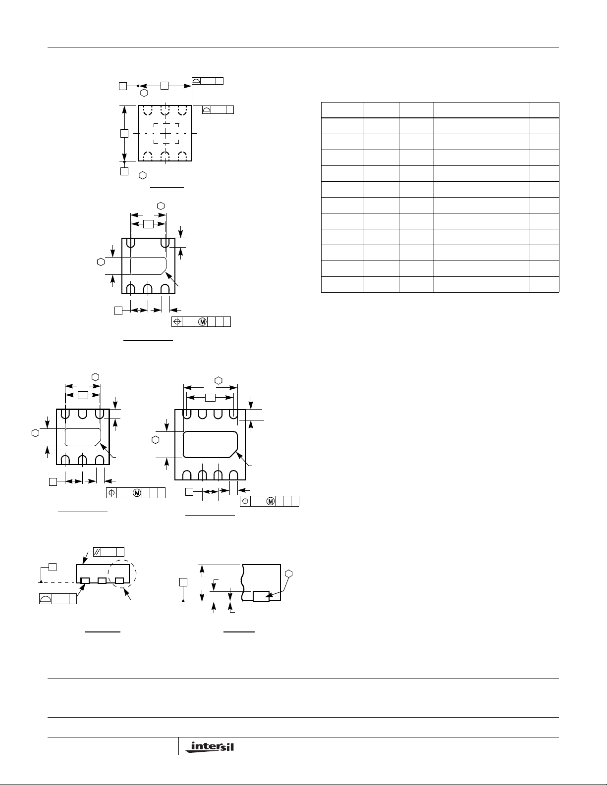
Optical Dual Flat No-Lead Family (ODFN)
0.10 C
2X
TYP.
L
PIN
#1 I.D.
b
0.10 C A B
0.10 C
2X
3
(E2)
e
A
E
B
BOTTOM VIEW
5 LD ODFN
(2.0x2.1 BODY)
D
4
54
12 3
5
TOP VIEW
3
(D2)
e1
45
123
ISL29002
MDP0052
OPTICAL DUAL FLAT NO-LEAD FAMILY
SYMBOL ODFN5 ODFN6 ODFN8 TOLERANCE NOTE
A 0.70 0.70 0.70 ±0.05
A1 0.02 0.02 0.02 +0.03/-0.02
b 0.30 0.30 0.30 ±0.05
c 0.20 0.20 0.20 Reference 2
D 2.00 2.00 3.00 Basic
D2 1.35 1.35 2.29 Reference 3
E 2.10 2.10 3.00 Basic
E2 0.65 0.65 1.40 Reference 3
e 0.65 0.65 0.65 Basic
e1 1.30 1.30 1.95 Basic
L 0.35 0.35 0.40 ±0.05
Rev. 4 5/06
NOTES:
1. Dimensioning and tolerancing per ASME Y14.5M-1994.
2. Exposed lead at side of package is a non-functional feature.
3. Dimension D2 and E2 define the size of the exposed pad.
4. ODFN 5 Ld version has no center lead (shown as dashed line).
(D2)
46
3
(E2)
e
BOTTOM VIEW
6 LD ODFN
(2.0x2.1 BODY)
C
SEATIN G
PLANE
0.08 C
(ALL LEADS
& EXPOSED PAD)
3
e1
5
123
SIDE VIEW
TYP.
L
PIN
#1 I.D.
b
0.10 C A B
0.10 C
DETAIL "X"
SEE
3
(E2)
4
BOTTOM VIEW
(3.0x3.0 BODY)
C
(D2)
e1
5
3 261
e
8 LD ODFN
A
3
7
(C)
DETAIL X
8
TYP.L
PIN
#1 I.D.
b
0.10 C A B
A1
2
All Intersil U.S. products are manufactured, assembled and tested utilizing ISO9000 quality systems.
Intersil Corporation’s quality certifications can be viewed at www.intersil.com/design/quality
Intersil products are sold by description only. Intersil Corporation reserves the right to make changes in circuit design, software and/or specifications at any time without
notice. Accordingly, the reader is cautioned to verify that data sheets are current before placing orders. Information furnished by Intersil is believed to be accurate and
reliable. However, no responsibility is assumed by Intersil or its subsidiaries for its use; nor for any infringements of patents or other rights of third parties which may result
from its use. No license is granted by implicat ion or oth erwise u nde r any p a tent or p at ent r ights of Intersil or its subsidiaries.
For information regarding Intersil Corporation and its products, see www.intersil.com
10
FN7465.2
December 1, 2006
 Loading...