


查询ISL29001IROZ供应商
®
ISL29001
Data Sheet December 21, 2005
Ambient Light Sensor
The ISL29001 is an integrated ambient light sensor with
ADC and I2C interface. With a spectral sensitivity curve
matched to that of the human eye, the ISL29001 provides
15-bit effective resolution while rejecting 50Hz and 60Hz
flicker caused by artificial light sources.
In normal operation, the ISL29001 consumes less than
300µA of supply current. A software power-down mode
controlled via the I
2
C interface disables all but the I2C
interface. A power-down pin is also provided which reduces
power consumption to less than 1µA.
The ISL29001 includes an internal oscillator which provides
100ms automatic integration periods, or can be externally
timed by I
2
C commands. Both the internal timing and the
illuminance resolution can be adjusted with an external
resistor.
Designed to operate on supplies from 2.5V to 3.3V, the
ISL29001 is specified for operation over the -40°C to +85°C
ambient temperature range. It is packaged in a clear 6-pin
ODFN package.
Ordering Information
PAR T
NUMBER PACKAGE TAPE & REEL PKG. DWG. #
ISL29001IROZ
(See Note)
NOTE: Intersil Pb-free plus anneal products employ special Pb-free
material sets; molding compounds/die attach materials and 100%
matte tin plate termination finish, which are RoHS compliant and
compatible with both SnPb and Pb-free soldering operations. Intersil
Pb-free products are MSL classified at Pb-free peak reflow
temperatures that meet or exceed the Pb-free requirements of
IPC/JEDEC J STD-020.
6-Pin ODFN
(Pb-Free)
- MDP0052
FN6166.0
Features
• Human eye response
• Temperature compensated
• 15-bit effective resolution
• Adjustable resolution: 3 to 15 counts per lux
• Simple output code, directly proportional to lux
• 0.3 lux to 10,000 lux range
• IR rejection
• 50Hz/60Hz rejection
2
C interface
•I
• 2.5V to 3.3V supply
• 6-pin ODFN (2.1mm x 2mm)
• Pb-Free plus anneal available (RoHS compliant)
Applications
• Ambient light sensing
• Ambient backlight control
• Temperature control systems
• Contrast control
• Camera light meters
• Lighting controls
•HVAC
Block Diagram
V
DD
PD
Pinout
VDD
GND
REXT
ISL29001
(6-PIN ODFN)
TOP VIEW
1
THERMAL
2
PAD
3
1
TEMPERATURE
COMPENSATED
LIGHT SENSOR
6
SDA
SCL
5
PD
4
CAUTION: These devices are sensitive to electrostatic discharge; follow proper IC Handling Procedures.
1-888-INTERSIL or 1-888-468-3774
| Intersil (and design) is a registered trademark of Intersil Americas Inc.
All other trademarks mentioned are the property of their respective owners.
Copyright © Intersil Americas Inc. 2005. All Rights Reserved.
50Hz/60Hz
REJECTION
GND
16-bit
ADC
R
EXT
C INTERFACE
2
I
SDA
SCL

ISL29001
Absolute Maximum Ratings (T
Maximum Supply Voltage between V
2
I
C Bus Pin Voltage (SCL, SDA) . . . . . . . . . . . . . . . . . -0.2V to 5.5V
2
I
C Bus Pin Current (SCL, SDA) . . . . . . . . . . . . . . . . . . . . . . <10mA
R
Pin Voltage. . . . . . . . . . . . . . . . . . . . . . . . . . . . . . -0.2V to 3.6V
ext
Operating Temperature . . . . . . . . . . . . . . . . . . . . . . . -45°C to +85°C
CAUTION: Stresses above those listed in “Absolute Maximum Ratings” may cause permanent damage to the device. This is a stress only rating and operation of the
device at these or any other conditions above those indicated in the operational sections of this specification is not implied.
IMPORTANT NOTE: All parameters having Min/Max specifications are guaranteed. Typical values are for information purposes only. Unless otherwise noted, all tests
are at the specified temperature and are pulsed tests, therefore: T
Electrical Specifications V
= 25°C)
A
and GND . . . . . . . . . . 3.6V
DD
= 3V, TA = 25°C, R
DD
specified.
Maximum Die Temperature . . . . . . . . . . . . . . . . . . . . . . . . . . +125°C
Storage Temperature . . . . . . . . . . . . . . . . . . . . . . . . -45°C to +100°C
ESD Voltage . . . . . . . . . . . . . . . . . . . . . . . . . . . . . . . . . . . . . . . . 2kV
= TC = T
J
A
= 100kΩ, internally controlled integration timing (Note 1), unless otherwise
EXT
PARAMETER DESCRIPTION CONDITION MIN TYP MAX UNIT
V
I
DD
I
DD1
I
DD2
DD
Power Supply Range 2.25 3.63 V
Supply Current 0.28 0.33 mA
Supply Current Software disabled 0.09 0.10 mA
Supply Current PD = 3V 0.5 µA
FUPD Internal Update Time Mode 1 & Mode 2 (Note 2) 85 105 126 ms
Fosc Internal Oscillator Frequency 312 kHz
2
FI
CI
2
C Clock Rate 1 400 kHz
DATA0 ADC Code Ev = 0 lux 1 Counts
DATA1 ADC Code Full scale ADC count value 32768 Counts
DATA2 ADC Code Ev = 300 lux, fluorescent light, Mode 1 738 983 1247 Counts
DATA3 ADC Code Ev = 300 lux, fluorescent light, Mode 2 98 Counts
V
REF
Voltage of R
Pin 0.487 0.51 0.532 V
EXT
NOTES:
1. See Principle of Operation
2. There are three modes of the ADC’s operations. In Mode 1, the ADC integrates the current of the photodiode which is sensitive to visible and
infrared light. In Mode 2, the ADC integrates the current of the photodiode which is sensitive only to infrared light.
Pin Descriptions
PIN NUMBER PIN NAME DESCRIPTION
1 VDD Positive supply. Connect this pin to a clean 2.5V to 3.3V supply.
2 GND Ground pin
3 PD Power-down pin. This pin is active-high. Applying a logic “high” to this pin will put the
4 REXT External resistor pin for ADC reference. Connect this pin to ground through a
5SCLI
6SDAI
2
device into power down mode.
(nominal) 100kΩ resistor.
2
C serial clock
2
C serial data
FN6166.0
December 21, 2005

ISL29001
Typical Performance Curves (Rext = 100kΩ)
320
Ta = 27oC
COMMAND = 00H
306
5000 lux
292
278
200 lux
264
SUPPLY CURRENT (µA)
250
2.0 2.3 2.6 2.9 3.2 3.5 3.8
SUPPLY VOLTAGE (V)
10
Ta = 27oC
COMMAND = 00H
8
0 lux
6
4
2
OUTPUT CODE (COUNTS)
0
2.0 2.3 2.6 2.9 3.2 3.5 3.8
SUPPLY VOLTAGE (V)
FIGURE 1. SUPPLY CURRENT vs SUPPLY VOLTAGE FIGURE 2. OUTPUT CODE FOR 0 LUX vs SUPPLY VOLTAGE
1.015
1.010
1.005
1.000
(% FROM 3V)
0.995
OUTPUT CODE RATIO
0.990
2.0 2.3 2.6 2.9 3.2 3.5 3.8
200 lux
SUPPLY VOLTAGE (V)
COMMAND = 00H
5000 lux
Ta = 27oC
320.0
319.5
319.0
318.5
318.0
OSCILLATOR FREQUENCY (kHz)
2.0 2.3 2.6 2.9 3.2 3.5 3.8
SUPPLY VOLTAGE (V)
Ta = 27oC
FIGURE 3. OUTPUT CODE vs SUPPLY VOLTAGE FIGURE 4. OSCILLATOR FREQUENCY vs SUPPLY VOLTAGE
315
Vdd = 3V
COMMAND = 00H
305
295
285
275
SUPPLY CURRENT (µA)
265
-60 -20 20 60 100
5000 lux
200 lux
TEMPERATURE (oC)
10
Vdd = 3V
COMMAND = 00H
8
0 lux
6
4
2
OUTPUT CODE (COUNTS)
0
-60 -20 20 60 100
TEMPERATURE (oC)
FIGURE 5. SUPPLY CURRENT vs TEMPERATURE FIGURE 6. OUTPUT CODE FOR 0 LUX vs TEMPERATURE
3
December 21, 2005
FN6166.0
ISL29001
Typical Performance Curves (Rext = 100kΩ) (Continued)
C)
o
1.080
1.048
1.016
Vdd = 3V
COMMAND = 00H
5000 lux
330
Vdd = 3V
329
328
200 lux
0.984
(% FROM 25
0.952
327
326
OUTPUT CODE RATIO
0.920
-60 -20 20 60 100
TEMPERATURE (oC)
325
OSCILLATOR FREQUENCY (kHz)
-60 -20 20 60 100
TEMPERATURE (oC)
FIGURE 7. OUTPUT CODE vs TEMPERATURE FIGURE 8. OSCILLATOR FREQUENCY vs TEMPERATURE
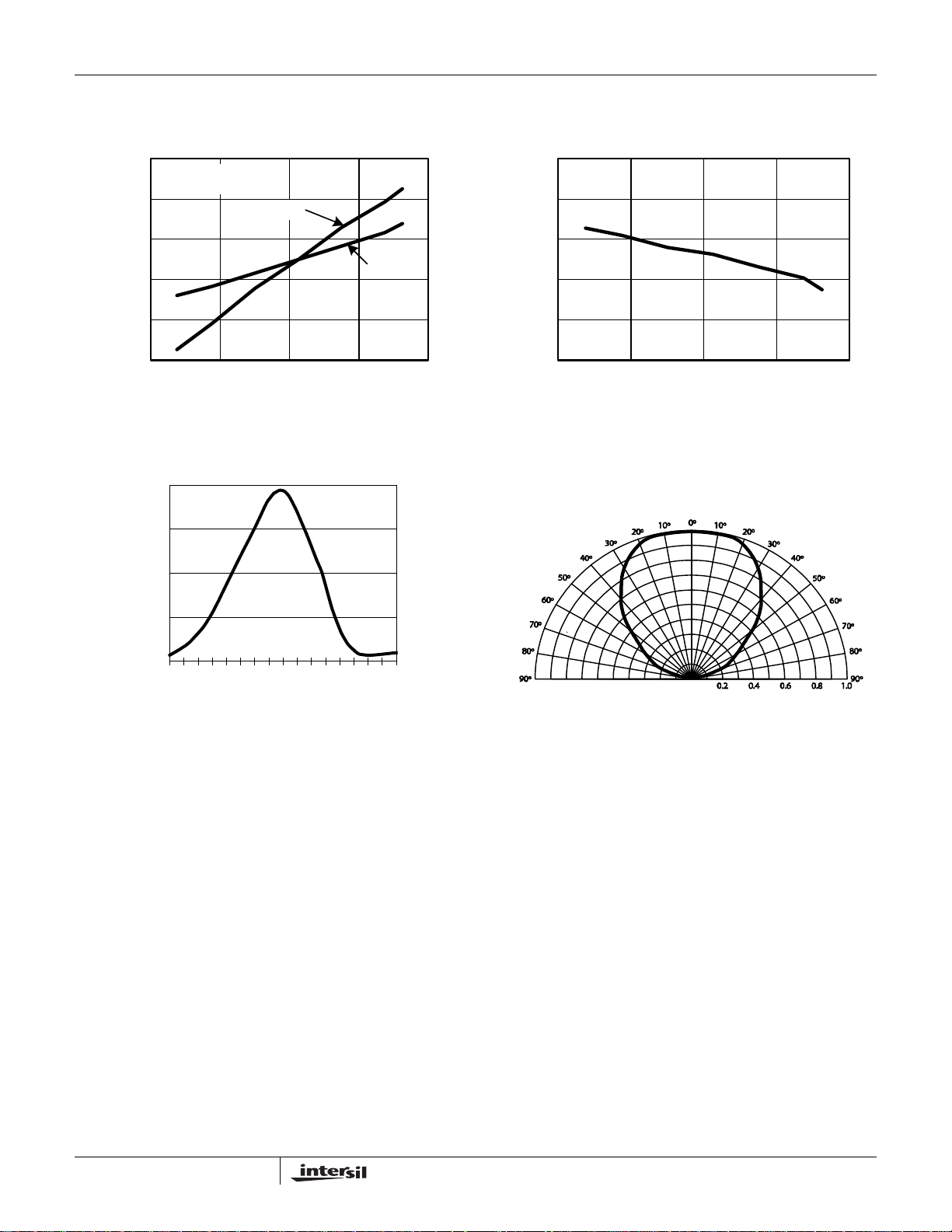
100
75
Diode 1
RADIATION PATTER N
LUMINOSITY
ANG LE
50
25
RELATIVE SENSITIVITY (%)
0
428
444
460
476
492
508
524
540
556
572
588
604
620
636
652
668
SPECTRAL WAVELENGTH (nm)
RELATIVE SENSITIVITY
FIGURE 9. RELATIVE SENSITIVITY FIGURE 10. RADIATION PATTERN
4
FN6166.0
December 21, 2005

ISL29001
Principles of Operation
Photodiodes and ADC
The ISL29001 contains two photodiodes. One of the
photodiodes is sensitive to visible and infrared light (Diode 1)
and the other is sensitive primarily to infrared light (Diode 2).
The ISL29001 also contains an on-chip integrating analogto-digital converter (ADC) to convert photodiode currents
into digital data.
The ADC has three operating modes with two timing
controls. (Please consult Table 1 for a complete list of
modes.) In the first operating mode, the ADC only integrates
Diode 1's current, and the digital output format is 16-bit
unsigned-magnitude. In second operating mode, the ADC's
operation is the same, except Diode 2's current is integrated.
In the third operating mode, the ADC integrates Diode 2's
current first, then Diode 1's current. The total integration time
is doubled, and the digital output is the difference of the two
photodiode currents (Diode 1’s current - Diode 2’s current).
In this mode, the digital output format is 16-bit 2'scomplement. Any of the three operating modes can be used
with either of the two timing controls (either internally or
externally controlled integration timing).
The interface to the ADC is implemented using the standard
2
I
C interface.
I2C Interface
The ISL29001 contains a single 8-bit command register that
can be written via the I
defines the operation of the device, which does not change
until the command register is overwritten.
The ISL29001 contains four 8-bit data registers that can be
read via the I
2
C interface. The first two data registers contain
the ADC's latest digital output, while the second two
registers contain the number of clock cycles in the previous
integration period.
The ISL29001’s I
1000100.
2
C interface. The command register
2
C address is hardwired internally as
master always drives the SCL (clock) line, while either the
master or the slave can drive the SDA (data) line. Every I
2
C
transaction begins with the master asserting a start condition
(SDA falling while SCL remains high). The following byte is
driven by the master, and includes the slave address and
read/write bit. The receiving device is responsible for pulling
SDA low during the acknowledgement period.
Any writes to the ISL29001 overwrite the command register,
changing the device’s mode. Any reads from the ISL29001
return two or four bytes of sensor data and counter value,
depending upon the operating mode. Neither the command
register nor the data registers have internal addresses, and
none of the registers can be individually addressed.
2
Every I
C transaction ends with the master asserting a stop
condition (SDA rising while SCL remains high).
For more information about the I
the Philips
® I2
C specification documents.
2
C standard, please consult
Command Register
The command register is used to define the ADC's
operations. Table 1 shows the primary commands used to
control the ADC.
Note that there are two classes of operating commands:
three for internal timing, and three for external (arbitrary)
timing.
When using any of the three internal timing commands, the
device self-times each conversion, which is nominally 100ms
(with
R
= 100kΩ).
EXT
When using any of the three external timing commands,
each command received by the device ends one conversion
and begins another. The integration time of the device is
thus the time between one I
the next. The integration time can be between 1 and 100
milliseconds. The external timing commands can be used to
2
C external timing command and
Figure 11 shows a sample one-byte read. (A typical
application will read two to four bytes, however.) The I
SDA DRIVEN BY MASTER SDA DRIVEN BY ISL29002
SDA
SCL
START
1-7 89
ADDRESS
5
R/W
FIGURE 11. I
2
C bus
ACK
2
C TIMING DIAGRAM
1-7 8 9
DATA
ACK
STOP
FN6166.0
December 21, 2005

ISL29001
synchronize the ADC’s integrating time to a PWM dimming
frequency in a backlight system in order to eliminate noise.
TAB L E 1 .
COMMAND FUNCTION
8cH ADC is powered-down.
0cH ADC is reset.
00H ADC converts Diode 1’s current (I
04H ADC converts Diode 2’s current (I
08H ADC converts I
30H ADC converts Diode 1’s current (I
34H ADC converts Diode 2’s current (I
38H ADC converts I
1xxx_xxxxB I
unsigned-magnitude 16-bit data. The
integration is internally timed at 100ms per
integration.
unsigned-magnitude 16-bit data. The
integration is internally timed at 100ms per
integration.
complement 16-bit data. The total integration
is internally timed at 200ms per integration.
unsigned-magnitude 16-bit data. The
integration is externally timed; each 30H
command sent to the device ends one
integration period and begins another.
unsigned-magnitude 16-bit data. The
integration is externally timed; each 34H
command sent to the device ends one
integration period and begins another.
complement 16-bit data. The integration is
externally timed; each 38H command sent to
the device ends one integration period and
begins another.
2
C communication test. The value written to
the command register can be read back via
2
the I
C bus.
DIODE1-IDIODE2
DIODE1-IDIODE2
into 2’s-
into 2’s-
DIODE1
DIODE2
DIODE1
DIODE1
) into
) into
) into
) into
The first two 8-bit data registers contain the most recent
sensor reading. The meaning of the specific value stored in
these data registers depends on the command written via
2
the I
C interface; see Table 1 for information on the various
commands. The first byte read over the I
2
C interface is the
least-significant byte; the second is the most significant. This
byte ordering is often called “little-endian” ordering.
The third and fourth 8-bit data registers contain the
integration counter value corresponding to the most recent
sensor reading. The ISL29001 includes a free-running
oscillator, each cycle of which increments a 16-bit counter. At
the end of each integration period, the value of this counter
is made available in these two 8-bit registers. Like the
sensor reading, the integration counter value is read across
2
the I
C bus in little-endian order.
Note that the integration counter value is only available
when using one of the three externally-timed operating
modes; when using internally-timed modes, the device will
NAK after the two-byte sensor reading has been read.
Internal Timing
When using one of the three internal timing modes, each
integration period of the ISL29001 is timed by 32,768 clock
cycles of an internal oscillator. The nominal frequency of the
internal oscillator is 327.6kHz, which provides 100ms
internally-timed integration periods. The oscillator frequency
is dependent upon an external resistor, R
adjusted by selecting a different resistor value. The
resolution and maximum range of the device are also
affected by changes in R
; see below.
ext
The oscillator frequency can be calculated with the following
equation:
100k Ω
f
osc
327.6k H z
------------------
⋅=
R
ext
, and can be
ext
Data Registers
The ISL29001 contains four 8-bit data registers. These
registers cannot be specifically addressed, as is
conventional with other I
a read operation on the device always returns all available
registers in ascending order. See Table 2 for a description of
each register.
ADDRESS CONTENTS
00H Least-significant byte of most recent sensor
reading.
01H Most-significant byte of most recent sensor
reading.
02H Least-significant byte of integration counter value
corresponding to most recent sensor reading.
03H Most-significant byte of integration counter value
corresponding to most recent sensor reading.
2
C peripherals; instead, performing
TABL E 2 .
6
R
is nominally 100kΩ, and provides 100 millisecond
ext
internal timing and a 1-10,000 lux range for Diode 1.
Doubling this resistor value to 200kΩ halves the internal
oscillator frequency, providing 200ms internal timing. In
addition, the maximum lux range of Diode 1 is also halved,
from 10,000 lux to 5,000 lux, and the resolution is doubled,
from 3.3 counts per lux to 6.6 counts per lux.
The acceptable range of this resistor is 50kΩ (providing
50ms internal timing, 100,000 lux maximum reading, ~1.6
counts per lux) to 500kΩ (500ms internal timing, 2,000 lux
maximum reading, ~16 counts per lux).
When using one of the three internal timing modes, the
ISL29001’s resolution is determined by the ratio of the max
lux range to 32,768, the number of clock cycles per
integration.
FN6166.0
December 21, 2005

ISL29001
The following equations describe the light intensity as a
function of the sensor reading, and the integration time as a
function of the external resistor.
----------------=
32768
---------------------------------------
100k Ω⁄()
R
ext
R
ext
------------------
⋅=
100k Ω
Data1⋅⋅
L
T 100m s
10 000 lux,
1
where L is the measured light intensity, Data1 is the sensor
reading, T is the integration time, and R
is external
ext
resistor value.
External Timing
When using one of the three external timing modes, each
integration period of the ISL29001 is determined by the time
which passes between consecutive external timing
commands received over the I
The internal oscillator operates identically in both the internal
and external timing modes, with the same dependence on
R
. However, when using one of the three external timing
ext
modes, the number of clock cycles per integration is no
2
C bus.
longer fixed at 32,768, but varies with the chosen integration
time.
The number of clock cycles in the previous integration period
is provided in the third and fourth bytes of data read across
2
the I
C bus. This two-byte value is called the integration
counter value.
When using one of the three external timing modes, the
ISL29001’s resolution varies with the integration time. The
resolution is determined by the ratio of the max lux range to
the number of clock cycles per integration.
The following equations describe the light intensity as a
function of sensor reading, integration counter value, and
integration time:
10 000lux,
---------------------------------------
L
100k Ω⁄()
R
ext
T = Time Interval between external time commands
Data1
-----------------
⋅=
Data2
where L is the measured light intensity, Data1 is the sensor
reading, Data2 is the integration counter value, T is the
integration time, and R
is external resistor value.
ext
Typical Circuit
A typical application circuit is shown in Figure 12.
2.5-
3.3V
4.7µF
ISL29002
VDD
+
0.1µF
VSS
FIGURE 12. TYPICAL CIRCUIT
SDA
SCL
REXTPD
100k
MICROCONTROLLER
SDA
SCL
7
FN6166.0
December 21, 2005

Suggested PCB Footprint
See Figure 13. Footprint pads should be a nominal 1-to-1
correspondence with package pads. The large, exposed
central die-mounting paddle in the center of the package
requires neither thermal nor electrical connection to the
PCB, and such connection should be avoided.
0.65
0.65
ISL29001
0.3
2.05
All dimensions in millimeters.
FIGURE 13. SUGGESTED PCB FOOTPRINT
Layout Considerations
The ISL29001 is relatively insensitive to layout. Like other
2
I
C devices, it is intended to provide excellent performance
even in significantly noisy environments. There are only a
few considerations that will ensure best performance.
Route the supply and I
sources of noise. Use two power-supply decoupling
capacitors, 4.7µF and 0.1µF, placed close to the device.
2
C traces as far as possible from all
Soldering Considerations
Convection heating is recommended for reflow soldering;
direct-infrared heating is not recommended. The ISL29001’s
plastic ODFN package does not require a custom reflow
soldering profile, and is qualified to 260°C. A standard reflow
soldering profile with a 260°C maximum is recommended.
8
FN6166.0
December 21, 2005

ODFN Package Outline Drawing
ISL29001
9
FN6166.0
December 21, 2005

ISL29001
All Intersil U.S. products are manufactured, assembled and tested utilizing ISO9000 quality systems.
Intersil Corporation’s quality certifications can be viewed at www.intersil.com/design/quality
Intersil products are sold by description only. Intersil Corporation reserves the right to make changes in circuit design, software and/or specifications at any time without
notice. Accordingly, the reader is cautioned to verify that data sheets are current before placing orders. Information furnished by Intersil is believed to be accurate and
reliable. However, no responsibility is assumed by Intersil or its subsidiaries for its use; nor for any infringements of patents or other rights of third parties which may result
from its use. No license is granted by implication or otherwise under any patent or patent rights of Intersil or its subsidiaries.
For information regarding Intersil Corporation and its products, see www.intersil.com
10
FN6166.0
December 21, 2005

Copyright © Each Manufacturing Company.
All Datasheets cannot be modified without permission.
This datasheet has been download from :
www.AllDataSheet.com
100% Free DataSheet Search Site.
Free Download.
No Register.
Fast Search System.
www.AllDataSheet.com
 Loading...