

Intersil ISL282x6EVAL1Z User Manual
®
ISL282x6EVAL1Z Evaluation Board User’s Guide
Application Note August 28, 2008
Introduction
The ISL282x6EVAL1Z evaluation board is a design platform
containing all the circuitry needed to characterize critical
performance parameters of the ISL282x6 operational
amplifiers in both MSOP-8 and SOIC-8 packages, using a
variety of user defined test circuits.
The ISL28236 and ISL28246 high-speed operational
amplifiers feature low power consumption, while ISL28256
and ISL28266 operational amplifiers feature ultra-low power
consumption. All op amps have rail-to-rail output drive
capability and are designed to operate with a single lithium
cell or two Ni_Cd batteries.
Reference Documents
• ISL28236 Data Sheet
• ISL28246 Data Sheet
• ISL28256 Data Sheet
• ISL28266 Data Sheet
Evaluation Board Key Features
The ISL282x6EVAL1Z is designed to enable the IC to
operate from a single supply, +2.4VDC to +5.5VDC or from
split supplies, ±1.2VDC to ±2.75V. The board is configured
for a dual op amp connected for differential input with a
closed loop gain of 10. A single external reference voltage
(VREF) pin and provisions for a user-selectable voltage
divider - filter are included.
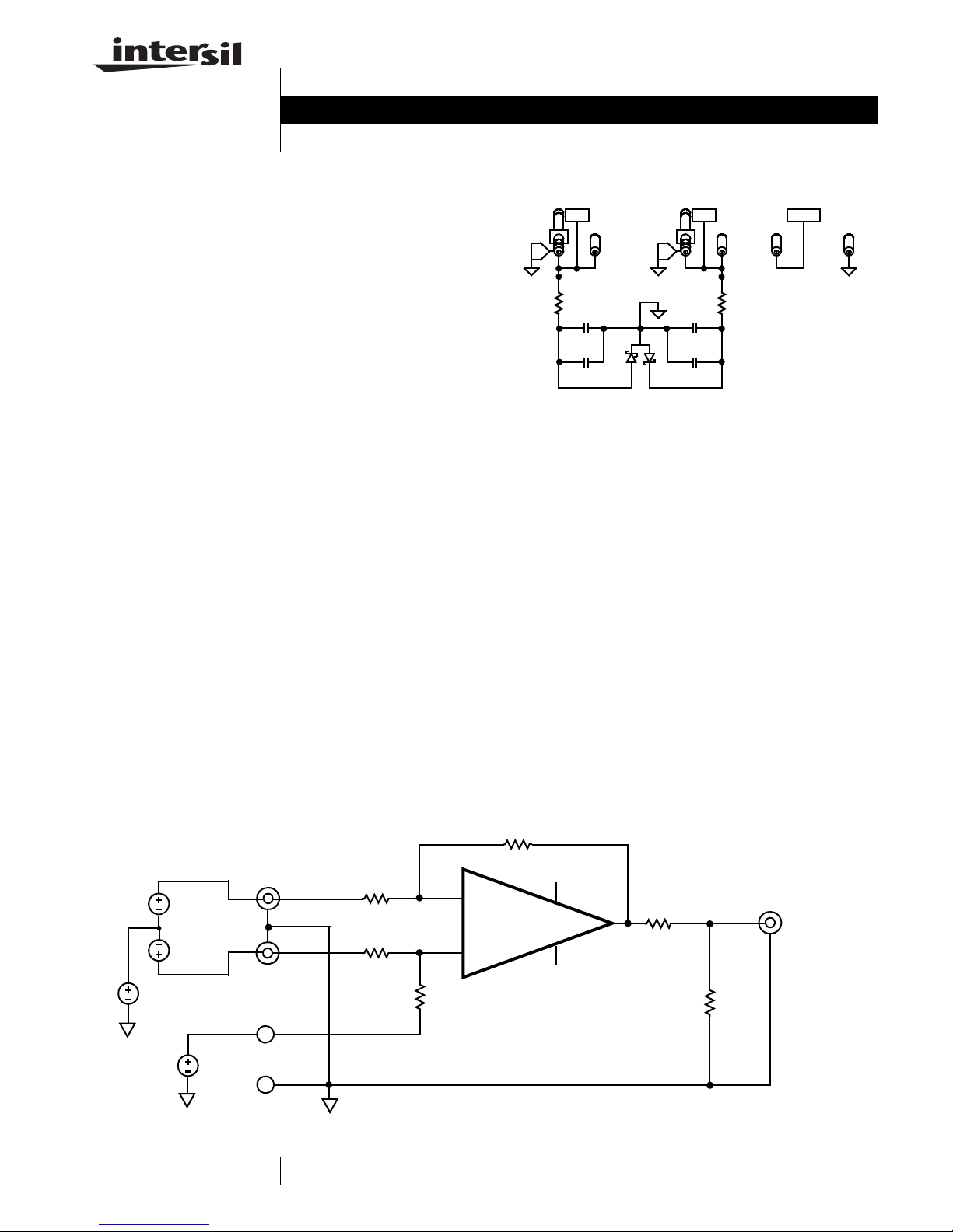
Power Supplies (Figure 1)
External power connections are made through the +V, -V,
VREF and Ground connections on the evaluation board.
AN1420.0
J6
J8
0
R16
C2 C4
C3
FIGURE 1. POWER SUPPLY CIRCUIT
User selectable SMA edge connectors are also provided for
+V and -V. For single supply operation, the -V and Ground
pins are tied together to the power supply negative terminal.
For split supplies, +V and -V terminals connect to their
respective power supply terminals. De-coupling capacitors
C
and C4 connect to their respective supplies through R16
2
and R
0Ω resistors. These resistors are 0Ω but can be
31
changed by the user to provide additional power supply
filtering, or to reduce the voltage rate-of-rise to less than
±1V/µs. Two additional capacitors, C
close to the part to filter out high frequency noise.
Anti-reverse diode D
accidental polarity reversal.
J11
V+V-
J12
0
R31
4.7µF4.7µF
C5
0.01µF0.01µF
D1
and C5 are connected
3
protects the circuit in the case of
1
VREF
J13
J14
Amplifier Configuration (Figure 2)
The schematic of 1/2 of the op amp with the components
supplied is shown in Figure 2. The circuit implements a
differential input amp with a closed loop gain of 10. The
circuit can operate from a single supply or from dual
supplies. The VREF pin must be connected to ground to
IN -
IN-
IN+
IN +
VCM
VREF
VREF
GND
1
RF
100k
Ω
RIN-
10k
Ω
RIN+
10k
Ω
FIGURE 2. BASIC AMPLIFIER CONFIGURATION
IN-
-
IN+
+
R
+
REF
100k
Ω
CAUTION: These devices are sensitive to electrostatic discharge; follow proper IC Handling Procedures.
1-888-INTERSIL or 1-888-468-3774
VP
V+
V-
VM
| Intersil (and design) is a registered trademark of Intersil Americas Inc.
All other trademarks mentioned are the property of their respective owners.
ISL282x6 (1/2)
0
Ω
RL
10k
Ω
Copyright Intersil Americas Inc. 2008. All Rights Reserved
VOUT

Application Note 1420
establish a ground referenced input for dual supply
operation, or can be externally set to any reference level for
single supply operation. VREF should not be left floating.
User-selectable Options (Figures 3 and 4)
Component pads are included to enable a variety of
user-selectable circuits to be added to the amplifier VREF,
inputs, outputs, and the amplifier feedback loops. The inputs
(Figure 3) have additional resistor and capacitor, and jumper
placements for loading and/or measurement of frequency
sensitive parameters.
R18R15
100k
OUTNODEIN+
R12R10
R13R11
C1
OPEN
R14
VREF
R17
IN-
DNP DNP
R6
DNP
10k 100k
R5
DNP
10k
DNP
R3
R4
0
DNP
J1
J2
R1
DNP
R2
DNP
DNP
TO OUTPUT
TO IN-
TO IN+
The outputs (see Figure 4) have a 10kΩ load resistor to
ground and have additional resistor and capacitor
placements for loading.
Note: Operational amplifiers are sensitive to output
capacitance and may oscillate. In the event of oscillation,
reduce output capacitance by using shorter cables or add a
resistor in series with the output.
FROM OUTPUT
C6
OPEN
R26
0
C8
OPEN
R28
10k
FIGURE 3. INPUT STAGE (1/2) FIGURE 4. OUTPUT STAGE (1/2)
2
AN1420.0
August 28, 2008
 Loading...