

Page 1
®
ISL28274, ISL28474
Data Sheet August 17, 2007
Micropower, Single Supply, Rail-to-Rail
Input-Output Instrumentation Amplifier
and Precision Operational Amplifier
The ISL28274 is a combination of a micropower
instrumentation amplifier (Amp A) with a low power precision
amplifier (Amp B) in a single package. The ISL28474
consists of two micropower instrumentation amplifiers
(Amp A) and two low power precision amplifiers (Amp B) in a
single package. The amplifiers are optimized for operation at
2.4V to 5V single supplies. Inputs and outputs can operate
rail-to-rail. As with all instrumentation amplifiers, a pair of
inputs provide a high common-mode rejection and are
completely independent from a pair of feedback terminals.
The feedback terminals allow zero input to be translated to
any output offset, including ground. A feedback divider
controls the overall gain of the amplifier. The additional
precision amplifier can be used to generate higher gain, with
smaller feedback resistors or used to generate a reference
voltage.
The instrumentation amp (Amp A) is compensated for a gain
of 100 or more and the precision amp (Amp B) is unity gain
stable. Both amplifiers have PMOS inputs that provide less
than 30pA input bias currents.
FN6345.2
Features
• Combination of IN-AMP and OP-AMP in a single package
• 120µA supply current for ISL28274
• Input offset voltage IN-AMP 500µV max
• Input offset voltage OP-AMP 225µV max
• 30pA max input bias current
• 100dB CMRR and PSRR
• Single supply operation of 2.4V to 5.0V
• Ground sensing
• Input voltage range is rail-to-rail and output swings
rail-to-rail
• Pb-free available (RoHS compliant)
Applications
• 4mA to 20mA loops
• Industrial process control
• Medical instrumentation
The amplifiers can be operated from one lithium cell or two
Ni-Cd batteries. The amplifiers input range goes from below
ground to slightly above positive rail. The output stage
swings completely to ground or positive supply; no pull-up or
pull-down resistors are needed.
Ordering Information
PART NUMBER
(Note)
ISL28274FAZ* 28274 FAZ 16 Ld QSOP MDP0040
ISL28474FAZ* ISL28474 FAZ 24 Ld QSOP MDP0040
*Add “-T7” suffix for tape and reel. Please refer to TB347 for details
on reel specifications.
NOTE: These Intersil Pb-free plastic packaged products employ
special Pb-free material sets; molding compounds/die attach
materials and 100% matte tin plate PLUS ANNEAL - e3 termination
finish, which is RoHS compliant and compatible with both SnPb and
Pb-free soldering operations. Intersil Pb-free products are MSL
classified at Pb-free peak reflow temperatures that meet or exceed
the Pb-free requirements of IPC/JEDEC J STD-020.
PART
MARKING
PACKAGE
(Pb-free)
PKG.
DWG. #
1
CAUTION: These devices are sensitive to electrostatic discharge; follow proper IC Handling Procedures.
1-888-INTERSIL or 1-888-468-3774
| Intersil (and design) is a registered trademark of Intersil Americas Inc.
Copyright © Intersil Americas Inc. 2006, 2007. All Rights Reserved.
All other trademarks mentioned are the property of their respective owners.
Page 2
Pinout
ISL28274
(16 LD QSOP)
TOP VIEW
ISL28274, ISL28474
ISL28474
(24 LD QSOP)
TOP VIEW
1
NC
IA OUT
2
IA FB+
3
A
-+
B
IA FB-
4
IA IN- IN-
5
IA IN+
6
IA EN
7
8 9
V- NC
IA = Instrumentation Amplifier
= Instrumentation Amplifier
A
-+
= Precision Amplifier
B
-+
-+
16
V+
OUT
15
NC
14
NC
13
12
11
IN+
EN
10
IA OUT_1
IA FB+_1
IA FB-_1
IA IN-_1
IA IN+_1 IA IN+_2
IA EN
1
2
A
-+
3
4
5
6
_1
V+
7
EN
8 17
_1 EN_2
IN+_1 IN+_2
9
IN-_1
10
NC
OUT_1 OUT_2
IA = Instrumentation Amplifier
A
-+
-+
B
-+
11
12
B
= Instrumentation Amplifier
= Precision Amplifier
A
B
-+
-+
24
IA OUT_2
IA FB+_2
23
IA FB-_2
22
IA IN-_2
21
20
19
IA EN_2
V-
18
16
IN-_2
15
NC
14
13
2
FN6345.2
August 17, 2007
Page 3
ISL28274, ISL28474
Absolute Maximum Ratings (T
Supply Voltage. . . . . . . . . . . . . . . . . . . . . . . . . . . . . . . . . . . . . . 5.5V
Supply Turn On Voltage Slew Rate . . . . . . . . . . . . . . . . . . . . . 1V/μs
Input Current (IN, FB) . . . . . . . . . . . . . . . . . . . . . . . . . . . . . . . . 5mA
Differential Input Voltage (IN, FB) . . . . . . . . . . . . . . . . . . . . . . . 0.5V
Input Voltage . . . . . . . . . . . . . . . . . . . . . . . . . V-
ESD Rating
Human Body Model . . . . . . . . . . . . . . . . . . . . . . . . . . . . . . . . .3kV
Machine Model. . . . . . . . . . . . . . . . . . . . . . . . . . . . . . . . . . . .300V
= +25°C) Thermal Information
A
Thermal Resistance θ
16 Ld QSOP Package . . . . . . . . . . . . . . . . . . . . . . . 112
24 Ld QSOP Package . . . . . . . . . . . . . . . . . . . . . . . 88
- 0.5V to V+ + 0.5V
Output Short-Circuit Duration . . . . . . . . . . . . . . . . . . . . . . .Indefinite
Ambient Operating Temperature Range . . . . . . . . .-40°C to +125°C
Storage Temperature Range . . . . . . . . . . . . . . . . . .-65°C to +150°C
Operating Junction Temperature . . . . . . . . . . . . . . . . . . . . .+125°C
Pb-free reflow profile . . . . . . . . . . . . . . . . . . . . . . . . . .see link below
(°C/W)
JA
http://www.intersil.com/pbfree/Pb-FreeReflow.asp
CAUTION: Do not operate at or near the maximum ratings listed for extended periods of time. Exposure to such conditions may adversely impact product reliability and
result in failures not covered by warranty.
IMPORTANT NOTE: All parameters having Min/Max specifications are guaranteed. Typical values are for information purposes only. Unless otherwise noted, all tests
are at the specified temperature and are pulsed tests, therefore: T
Electrical Specifications INSTRUMENTATION AMPLIFIER “A” V
= TC = T
J
A
= +5V, V- = GND, VCM = 1/2V+, TA = +25°C, unless otherwise
+
specified. For ISL28274 ONLY. Boldface limits apply over the operating temperature range, -40°C to +125°C,
temperature data established by characterization
PARAMETER DESCRIPTION CONDITIONS
V
OS
Input Offset Voltage ISL28274 -400
ISL28474 -500
TCV
Input Offset Voltage
OS
Temperature = -40°C to +125°C 3 µV/°C
MIN
(Note 1) TYP
-750
-750
MAX
(Note 1) UNIT
35 400
750
35 500
750
µV
µV
Temperature Coefficient
I
OS
Input Offset Current
between IN+ and IN-, and
(see Figure 44 for extended temperature range)
-40°C to +85°C
-30
-80
±530
80
pA
between FB+ and FB-
I
B
e
N
Input Bias Current (IN+, IN, FB+, and FB- terminals)
(see Figure 36 and 37 for extended temperature range)
-40°C to +85°C
-30
-80
±10 30
80
Input Noise Voltage f = 0.1Hz to 10Hz 6 µV
pA
P-P
Input Noise Voltage Density fo = 1kHz 78 nV/√Hz
i
N
R
IN
V
IN
CMRR Common Mode Rejection
PSRR Power Supply Rejection
E
G
SR Slew Rate R
GBWP Gain Bandwidth Product V
Input Noise Current Density fo = 1kHz 0.19 pA/√Hz
Input Resistance 1GΩ
Input Voltage Range V+ = 2.4V to 5.0V 0 V
V
Ratio
Ratio
= 0V to 5V 80
CM
V
= 2.4V to 5V 80
+
75
75
100 dB
100 dB
+
V
Gain Error RL = 100kΩ to 2.5V -0.2 %
= 1kΩ to VCM ISL28274 0.40
L
ISL28474 0.40
OUT
= 10mV
; RL = 10kΩ 6MHz
P-P
0.35
0.35
0.5 0.65
0.70
0.5 0.7
0.75
V/µs
V/µs
3
FN6345.2
August 17, 2007
Page 4
ISL28274, ISL28474
Electrical Specifications OPERATIONAL AMPLIFIER “B” V
= +5V, V- = GND, VCM = 1/2V+, TA = +25°C, unless otherwise specified.
+
For ISL28274 ONLY. Boldface limits apply over the operating temperature range, -40°C to +125°C.
PARAMETER DESCRIPTION CONDITIONS
V
OS
ΔV
OS
------------------
ΔTi me
ΔV
OS
--------------- -
ΔT
I
OS
I
B
e
N
Input Offset Voltage -225
Long Term Input Offset Voltage
Stability
Input Offset Drift vs Temperature 2.2 µV/°C
Input Offset Current (see Figure 46 for extended temperature range)
-40°C to +85°C
Input Bias Current (see Figures 40 and 41 for extended temperature range)
-40°C to +85°C
Input Noise Voltage Peak-to-Peak f = 0.1Hz to 10Hz 5.4 µV
MIN
(Note 1) TYP
±20 225
-450
1.2 µV/Mo
-30
-80
-30
±10 30
-80
MAX
(Note 1) UNIT
450
±530
Input Noise Voltage Density fO = 1kHz 50 nV/√Hz
i
N
Input Noise Current Density fO = 1kHz 0.14 pA/√Hz
CMIR Input Voltage Range Guaranteed by CMRR test 05V
CMRR Common-Mode Rejection Ratio V
PSRR Power Supply Rejection Ratio V
A
VOL
Large Signal Voltage Gain VO = 0.5V to 4.5V, RL = 100kΩ 200
SR Slew Rate R
GBW Gain Bandwidth Product V
= 0V to 5V 80
CM
= 2.4V to 5V 85
+
= 1kΩ to VCM 0.12
L
OUT
= 10mV
; RL = 10kΩ 300 kHz
P-P
75
80
190
0.09
100 dB
105 dB
300 V/mV
±0.14 0.16
0.21
µV
pA
80
pA
80
P-P
V/µs
Electrical Specifications COMMON ELECTRICAL SPECIFICATIONS V
specified. For ISL28274 ONLY. Boldface limits apply over the operating temperature range, -40°C to +125°C.
PARAMETER DESCRIPTION CONDITIONS
V
OUT
I
S,ON
I
S,OFF
I
SC
Maximum Output Voltage Swing Output low, RL = 100kΩ to VCM 3 6
Output low, R
Output high, R
Output high, R
= 1kΩ to VCM 130 175
L
= 100kΩ to VCM 4.990
L
= 1kΩ to VCM 4.800
L
Supply Current, Enabled ISL28274 All channels enabled 120 156
ISL28474 All channels enabled 240 315
Supply Current, Disabled ISL28274 All channels disabled 4 7
ISL28474 All channels disabled 10 15
+ Short Circuit Sourcing Capability RL = 10Ω to VCM 28
= 5V, V- = GND, VCM = 1/2V+, TA = +25°C, unless otherwise
+
MIN
(Note 1) TYP
MAX
(Note 1) UNIT
mV
30
mV
225
4.996 V
4.97
4.880 V
4.750
µA
175
µA
350
µA
9
µA
20
31 mA
24
4
FN6345.2
August 17, 2007
Page 5
ISL28274, ISL28474
Electrical Specifications COMMON ELECTRICAL SPECIFICATIONS V
specified. For ISL28274 ONLY. Boldface limits apply over the operating temperature range, -40°C to +125°C.
= 5V, V- = GND, VCM = 1/2V+, TA = +25°C, unless otherwise
+
(Continued)
MIN
PARAMETER DESCRIPTION CONDITIONS
(Note 1) TYP
ISC- Short Circuit Sinking Capability RL = 10Ω to VCM 24
20
V
V
V
I
ENH
I
ENL
+
INH
INL
Minimum Supply Voltage 2.4 V
Enable Pin High Level 2 V
Enable Pin Low Level 0.8 V
Enable Pin Input Current VEN = 5V 0.8 1
Enable Pin Input Current VEN = 0V 0
NOTE:
1. Parts are 100% tested at +25°C. Over temperature limits established by characterization and are not production tested.
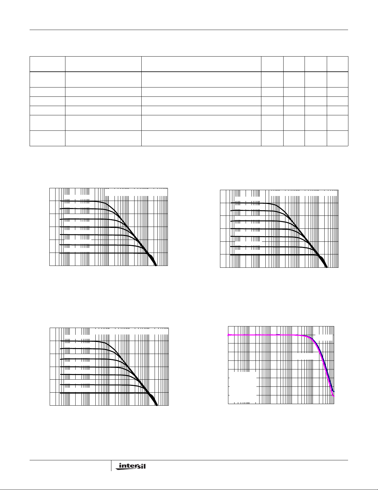
Typical Performance Curves V
90
80
70
60
GAIN (dB)
50
40
GAIN = 10,000
GAIN = 5,000
GAIN = 2,000
GAIN = 1,000
GAIN = 500
GAIN = 200
GAIN = 100
COMMON-MODE INPUT = V
= +5V, V- = GND, VCM = 1/2V+, TA = +25°C, unless otherwise specified.
+
+
90
80
70
60
GAIN (dB)
50
40
GAIN = 10,000
GAIN = 5,000
GAIN = 2,000
GAIN = 1,000
GAIN = 500
GAIN = 200
GAIN = 100
COMMON-MODE INPUT = 1/2V
MAX
(Note 1) UNIT
26 mA
µA
1.3
26
50
100
µA
+
30
1 10 100 1k 10k 100k 1M
FREQUENCY (Hz)
FIGURE 1. AMPLIFIER “A” (IN-AMP) FREQUENCY
RESPONSE vs CLOSED LOOP GAIN
90
80
70
60
GAIN (dB)
50
40
30
GAIN = 10,000
GAIN = 5,000
GAIN = 2,000
GAIN = 1,000
GAIN = 500
GAIN = 200
GAIN = 100
1 10 100 1k 10k 100k 1M
COMMON-MODE INPUT = VM +10mV
FREQUENCY (Hz)
FIGURE 3. AMPLIFIER “A” (IN-AMP) FREQUENCY
RESPONSE vs CLOSED LOOP GAIN
30
1 10 100 1k 10k 100k 1M
FREQUENCY (Hz)
FIGURE 2. AMPLIFIER “A” (IN-AMP) FREQUENCY
RESPONSE vs CLOSED LOOP GAIN, V
45
40
35
30
25
20
GAIN (dB)
15
10
5
0
10
AV = 100
= 10kΩ
R
L
= 10pF
C
L
= 100
R
F/RG
= 10kΩ
R
F
= 100Ω
R
G
100 10k1k 100k 1M
FREQUENCY (Hz)
V
= 2.4V
+
V+ = 5V
FIGURE 4. AMPLIFIER “A” (IN-AMP) FREQUENCY
RESPONSE vs SUPPLY VOLTAGE
CM
= 1/2V
+
5
FN6345.2
August 17, 2007
Page 6
ISL28274, ISL28474
Typical Performance Curves V
50
45
40
35
GAIN (dB)
30
25
AV = 100
= 10kΩ
R
= 10pF
C
L
R
F/RG
= 10kΩ
R
F
= 100Ω
R
G
10
= 100
100 10k1k 100k 1M
FREQUENCY (Hz)
= +5V, V- = GND, VCM = 1/2V+, TA = +25°C, unless otherwise specified. (Continued)
+
2200pF
1200pF
820pF
56pF
FIGURE 5. AMPLIFIER “A” (IN-AMP) FREQUENCY
RESPONSE vs C
120
100
80
60
PSRR (dB)
40
AV = 100
20
0
10 100 1k 10k 100k 1M
LOAD
PSRR+
PSRR-
FREQUENCY (Hz)
FIGURE 7. AMPLIFIER “A” (IN-AMP) PSRR vs FREQUENCY
120
100
80
60
CMRR (dB)
AV = 100
40
20
0
10 100 1k 10k 100k
FREQUENCY (Hz)
1M
FIGURE 6. AMPLIFIER “A” (IN-AMP) CMRR vs FREQUENCY
700
600
500
400
300
200
100
INPUT VOLTAGE NOISE (nV/ √Hz)
0
1 10 100 1k 10k 100k
AV = 100
FREQUENCY (Hz)
FIGURE 8. AMPLIFIER “A” (IN-AMP) INPUT VOLTAGE NOISE
SPECTRAL DENSITY
2.0
1.8
1.6
1.4
1.2
1.0
0.8
0.6
0.4
CURRENT NOISE (pA/√Hz)
0.2
0.0
1 10 100 1k
AV = 100
10k
FREQUENCY (Hz)
FIGURE 9. AMPLIFIER “A” (IN-AMP) INPUT CURRENT
NOISE SPECTRAL DENSITY
6
100k
VOLTAGE NOISE (2µV/DIV)
TIME (1s/DIV)
FIGURE 10. AMPLIFIER “A” (IN-AMP) 0.1Hz TO 10Hz INPUT
VOLTAGE NOISE
FN6345.2
August 17, 2007
Page 7

ISL28274, ISL28474
Typical Performance Curves V
+1
0
V+, V- = ±2.5V
= 1k
R
L
V+, V- = ±2.5V
= 10k
R
L
P-P
10k 100k 1M
FREQUENCY (Hz)
GAIN (dB)
-1
-2
-3
-4
-5
-6
-7
8
1k
V
= 50mV
OUT
AV = 1
= 3pF
C
L
= 0/RG = INF
R
F
= +5V, V- = GND, VCM = 1/2V+, TA = +25°C, unless otherwise specified. (Continued)
+
V+, V- = ±1.2V
= 1k
R
L
V+, V- = ±1.2V
R
= 10k
L
FIGURE 11. AMPLIFIER “B” (OP-AMP) FREQUENCY
RESPONSE vs SUPPLY VOLTAGE
1000
800
600
400
200
(µV)
0
OS
V
-200
-400
-600
-800
-1000
-10123456
V+ = 5V
= OPEN
R
L
= 100k, RG = 100
R
F
A
= +1000
V
(V)
V
CM
FIGURE 13. INPUT OFFSET VOLT AGE vs COMMON MODE
INPUT VOLTAGE
5M
45
40
35
30
25
20
AV = 100
GAIN (dB)
15
= 10kΩ
R
L
= 3pF
C
L
10
= 100kΩ
R
F
= 1kΩ
R
5
G
0
100 10k 100k 1M
V+, V- = ±1.0V
1k
FREQUENCY (Hz)
V+, V- = ±2.5V
V+, V- = ±1.2V
FIGURE 12. AMPLIFIER “B” (OP-AMP) FREQUENCY
RESPONSE vs SUPPLY VOLTAGE
100
80
60
40
20
(pA)
0
-20
-BIAS
I
-40
-60
-80
-100
-10123456
V+ = 5V
= OPEN
R
L
= 100k, RG = 100
R
F
A
= +1000
V
V
(V)
CM
FIGURE 14. INPUT BIAS CURRENT vs COMMON-MODE
INPUT VOLTAGE
120
80
40
0
GAIN (dB)
-40
-80
1 1k 100k 10M
10
FREQUENCY (Hz)
10k 1M100
FIGURE 15. AMPLIFIER “B” (OP-AMP) A
@ 100kΩ LOAD
7
vs FREQUENCY
VOL
80
40
0
-40
-80
-120
100
80
60
40
PHASE (°)
GAIN (dB)
20
0
-20
10 10k 1M
100
FREQUENCY (Hz)
FIGURE 16. AMPLIFIER “B” (OP-AMP) A
@ 1kΩ LOAD
PHASE
GAIN
100k1k
vs FREQUENCY
VOL
200
150
100
50
0
-50
-100
-150
FN6345.2
August 17, 2007
PHASE (°)
Page 8

ISL28274, ISL28474
Typical Performance Curves V
10
V
= 5VDC
+
0
V
-10
RL = 10kΩ
-20
A
-30
-40
-50
PSRR (dB)
-60
-70
-80
-90
-100
10 100 1k 10k 100k
SOURCE
= +1
V
= 1V
P-P
PSRR -
TEMPERATURE (°C)
= +5V, V- = GND, VCM = 1/2V+, TA = +25°C, unless otherwise specified. (Continued)
+
PSRR +
1M
FIGURE 17. AMPLIFIER “B” (OP-AMP) PSRR vs FREQUENCY
2.56
V
IN
V
OUT
V
= 5VDC
+
V
= 0.1V
OUT
RL = 1kΩ
A
= +1
V
0 2 4 6 8 10 12 14 16 18 20
P-P
TIME (µs)
VOLTS (V)
2.54
2.52
2.50
2.48
2.46
2.44
2.42
FIGURE 19. AMPLIFIER “B” (OP-AMP) SMALL SIGNAL
TRANSIENT RESPONSE
10
0
-10
-20
-30
-40
-50
CMRR (dB)
-60
-70
-80
-90
-100
= ±2.5VDC
V
+, V-
V
RL = 10kΩ
10 100 1k 10k 100k
SOURCE
= 1V
P-P
TEMPERATURE (°C)
1M
FIGURE 18. AMPLIFIER “B” (OP-AMP) CMRR vs FREQUENCY
5
4
3
2
VOLTS (V)
1
0
-1
0 50 100 150 200 250
V
= 5VDC
+
V
= 2V
OUT
RL = 1kΩ
A
= -2
V
TIME (µs)
P-P
V
V
OUT
IN
FIGURE 20. AMPLIFIER “B” (OP-AMP) LARGE SIGNAL
TRANSIENT RESPONSE
10.00
1.00
0.10
CURRENT NOISE (pA/√Hz)
0.01
1 10 100 1k 10k
FREQUENCY (Hz)
100k
FIGURE 21. AMPLIFIER “B” (OP-AMP) CURRENT NOISE vs
FREQUENCY
8
1k
100
10
VOLTAGE NOISE (nV/√Hz)
1
1 10 100 10k 100k
FREQUENCY (Hz)
1k
FIGURE 22. AMPLIFIER “B” (OP-AMP) VOLTAGE NOISE vs
FREQUENCY
FN6345.2
August 17, 2007
Page 9

ISL28274, ISL28474
Typical Performance Curves V
V/DIV)
µ
VOLTAGE NOISE (1
5.4µV
P-P
= +5V, V- = GND, VCM = 1/2V+, TA = +25°C, unless otherwise specified. (Continued)
+
TIME (1s/DIV)
FIGURE 23. AMPLIFIER “B” (OP-AMP) 0.1Hz TO 10Hz INPUT
VOLTAGE NOISE
155
135
115
95
75
SUPPLY CURRENT (µA)
55
6
V
IN
V+ = 5V
5
4
3
VOLTS (V)
2
100K
100K
100K
VS +
VS +
100K
100K
100K
-
-
-
DUT
DUT
DUT
+
+
+
1K
1K
1K
VS -
VS -
Function
Function
Function
Genera tor
Genera tor
Genera tor
33140A
33140A
33140A
V
OUT
1
0
0 50 100 150 200
TIME (ms)
FIGURE 24. AMPLIFIER “B” (OP-AMP) INPUT VOLTAGE
SWING ABOVE THE V
EN
INPUT
1V/DIV0.1V/DIV
0
V
OUT
SUPPLY
+
AV = -1
V
= 200mV
IN
V+ = 5V
= 0V
V
-
P-P
35
2.0 3.5 4.0 5.5
2.5 5.04.53.0
SUPPLY VOLTAGE (V)
FIGURE 25. SUPPLY CURRENT vs SUPPLY VOLTAGE
170
n = 100
160
150
140
MEDIAN
MAX
130
120
110
CURRENT (µA)
100
90
80
-40 -20 0 20 40 60 80 100 120
MIN
TEMPERATURE (°C)
FIGURE 27. TOTAL SUPPLY CURRENT vs TEMPERATURE,
V
= ±2.5V ENABLED, RL = INF
+, V-
0
10µs/DIV
FIGURE 26. AMPLIFIER “B” (OP-AMP) ENABLE TO OUTPUT
DELAY TIME
5.0
n = 100
4.8
4.6
MAX
4.4
4.2
4.0
3.8
CURRENT (µA)
3.6
MEDIAN
3.4
3.2
3.0
-40 -20 0 20 40 60 80 100 120
MIN
TEMPERATURE (°C)
FIGURE 28. DISABLED POSITIVE SUPPLY CURRENT vs
TEMPERATURE, V
= ±2.5V, RL = INF
+, V-
9
FN6345.2
August 17, 2007
Page 10

ISL28274, ISL28474
Typical Performance Curves V
-4.0
n = 100
-4.5
-5.0
-5.5
CURRENT (µA)
-6.0
-6.5
-40 -20 0 20 40 60 80 100 120
MIN
TEMPERATURE (°C)
MEDIAN
= +5V, V- = GND, VCM = 1/2V+, TA = +25°C, unless otherwise specified. (Continued)
+
MAX
FIGURE 29. DISABLED NEGATIVE SUPPLY CURRENT vs
TEMPERATURE, V
40
20
0
-20
(pA)
-40
-60
BIAS
-80
-100
IA FB- I
-120
-140
-160
-40 -20 0 20 40 60 80 100 120
FIGURE 31. I
BIAS
MIN
TEMPERATURE (°C)
(IA FB-) vs TEMPERATURE, V
= ±2.5V, RL = INF
+, V-
MEDIAN
n = 100
MAX
+, V-
= ±2.5V.
50
0
-50
(pA)
-100
BIAS
-150
IA FB+ I
-200
-250
-300
-40 -20 0 20 40 60 80 100 120
FIGURE 30. I
25
-25
-75
(pA)
-125
BIAS
-175
IA FB+ I
-225
-275
-40 -20 0 20 40 60 80 100 120
FIGURE 32. I
MIN
TEMPERATURE (°C)
(IA FB+) vs TEMPERATURE, V
BIAS
TEMPERATURE (°C)
(IA FB+) vs TEMPERATURE, V
BIAS
MEDIAN
MEDIAN
MAX
MIN
MAX
+, V-
n = 100
+, V-
n = 100
= ±2.5V
= ±1.2V
50
0
-50
(pA)
-100
BIAS
-150
IA FB- I
-200
-250
-40-200 20406080100120
TEMPERATURE (°C)
FIGURE 33. I
(IA FB-) vs TEMPERATURE, V
BIAS
MEDIAN
MAX
10
MIN
n = 100
+, V-
= ±1.2V
50
0
-50
-100
(pA)
-150
BIAS
-200
IA IN+ I
-250
-300
-350
FIGURE 34. I
MEDIAN
-40 -20 0 20 40 60 80 100 120
TEMPERATURE (°C)
(IA IN+) vs TEMPERATURE, V
BIAS
n = 100
MIN
MAX
+, V-
August 17, 2007
= ±2.5V
FN6345.2
Page 11

OU
ISL28274, ISL28474
Typical Performance Curves V
50
0
-50
(pA)
-100
BIAS
-150
IA IN- I
-200
-250
-300
-40 -20 0 20 40 60 80 100 120
TEMPERATURE (°C)
FIGURE 35. I
50
0
-50
(pA)
-100
BIAS
-150
IA IN- I
-200
(IA IN-) vs TEMPERATURE, V
BIAS
MEDIAN
MIN
MEDIAN
= +5V, V- = GND, VCM = 1/2V+, TA = +25°C, unless otherwise specified. (Continued)
+
50
0
-50
(pA)
-100
BIAS
-150
IA IN+ I
-200
-250
-300
-40 -20 0 20 40 60 80 100 120
TEMPERATURE (°C)
FIGURE 36. I
50
0
-50
(pA)
-100
BIAS
-150
IN+ I
-200
(IA IN+) vs TEMPERATURE, V
BIAS
MEDIAN
MEDIAN
MIN
MAX
+, V-
MIN
MAX
MIN
MAX
MAX
+, V-
n = 100
= ±2.5V
n = 100
n = 100
= ±1.2V
n = 100
-250
-40 -20 0 20 40 60 80 100 120
TEMPERATURE (°C)
FIGURE 37. I
30
10
-10
-30
(pA)
-50
-70
BIAS
IN- I
-90
-110
-130
-150
-40 -20 0 20 40 60 80 100 120
FIGURE 39. I
(IA IN-) vs TEMPERATURE, V
BIAS
TEMPERATURE (°C)
(IN-) vs TEMPERATURE, V
BIAS
MEDIAN
MIN
MAX
+, V-
+, V-
n = 100
= ±2.5V
= ±1.2V
-250
-40 -20 0 20 40 60 80 100 120
FIGURE 38. I
40
-10
-60
-110
(pA)
BIAS
-160
IN+ I
-210
-260
-310
FIGURE 40. I
BIAS
-40-200 20406080100120
BIAS
TEMPERATURE (°C)
(IN+) vs TEMPERATURE, V
MIN
MEDIAN
TEMPERATURE (°C)
(IN+) vs TEMPERATURE, V
+, V-
MAX
+, V-
= ±2.5V
n = 100
= ±1.2V
11
FN6345.2
August 17, 2007
Page 12

ISL28274, ISL28474
Typical Performance Curves V
40
-10
-60
-110
(pA)
BIAS
-160
IN- I
-210
-260
-310
-40 -20 0 20 40 60 80 100 120
TEMPERATURE (°C)
FIGURE 41. I
50
40
30
20
10
(pA)
0
OS
IA I
-10
-20
-30
-40
-50
-40 -20 0 20 40 60 80 100 120
(IN-) vs TEMPERATURE, V
BIAS
MAX
TEMPERATURE (°C)
= +5V, V- = GND, VCM = 1/2V+, TA = +25°C, unless otherwise specified. (Continued)
+
n = 100
MIN
MEDIAN
MAX
= ±1.2V
+, V-
n = 100
MEDIAN
MIN
FIGURE 43. IA INPUT OFFSET CURRENT vs TEMPERA TURE,
V
= ±1.2V
+, V-
40.0
20.0
0.0
-20.0
(pA)
-40.0
OS
-60.0
IA I
-80.0
-100.0
-120.0
-140.0
-40 -20 0 20 40 60 80 100 120
TEMPERATURE (°C)
MAX
MEDIAN
n = 100
MIN
FIGURE 42. IA INPUT OFFSET CURRENT vs TEMPERATURE,
V
= ±2.5V
+, V-
100
50
0
-50
(pA)
OS
I
-100
-150
-200
-40 -20 0 20 40 60 80 100 120
MAX
MEDIAN
TEMPERATURE (°C)
n = 100
MIN
FIGURE 44. INPUT OFFSET CURRENT vs TEMPERATURE,
V
= ±2.5V
+, V-
40
20
0
-20
-40
-60
IOS (pA)
-80
-100
-120
-1400
-40 -20 0 20 40 60 80 100 120
TEMPERATURE (°C)
MAX
n = 100
MEDIAN
MIN
FIGURE 45. INPUT OFFSET CURRENT vs TEMPERATURE,
V
= ±1.2V
+, V-
12
800
600
400
200
(µV)
0
OS
-200
IA V
-400
-600
-800
-40 -20 0 20 40 60 80 100 120
MEDIAN
MAX
TEMPERATURE (°C)
n = 100
MIN
FIGURE 46. IA INPUT OFFSET VOLT AGE vs TEMPERATURE,
V
= ±2.5V
+, V-
FN6345.2
August 17, 2007
Page 13

ISL28274, ISL28474
Typical Performance Curves V
800
600
400
200
(µV)
0
OS
IA V
-200
-400
-600
-800
MEDIAN
-40 -20 0 20 40 60 80 100 120
MIN
MAX
TEMPERATURE (°C)
= +5V, V- = GND, VCM = 1/2V+, TA = +25°C, unless otherwise specified. (Continued)
+
n = 100
FIGURE 47. IA INPUT OFFSET VOLTAGE vs TEMPERATURE
V
= ±1.2V
+, V-
500
n = 100
400
300
200
100
(µV)
0
OS
-100
V
-200
-300
-400
-500
-40 -20 0 20 40 60 80 100 120
MEDIAN
MIN
MAX
TEMPERATURE (°C)
FIGURE 49. INPUT OFFSET VOLTAGE vs TEMPERATURE,
V
= ±1.2V
+, V-
500
n = 100
400
300
200
100
(µV)
0
OS
V
-100
-200
-300
-400
-500
-40 -20 0 20 40 60 80 100 120
MEDIAN
MIN
MAX
TEMPERATURE (°C)
FIGURE 48. INPUT OFFSET VOLT AG E vs TEMPERA TURE,
V
= ±2.5V
+, V-
145
135
125
115
105
IA CMRR (dB)
95
85
75
-40 -20 0 20 40 60 80 100 120
FIGURE 50. IA CMRR vs TEMPERATURE,
MIN
MEDIAN
MAX
TEMPERATURE (°C)
VCM = +2.5V TO
n = 100
-2.5V
140
130
120
110
CMRR (dB)
100
90
80
-40-200 20406080100120
MIN
MEDIAN
MAX
TEMPERATURE (°C)
n = 100
FIGURE 51. CMRR vs TEMPERATURE, VCM = +2.5V T O -2.5V
13
155
n = 100
145
135
125
115
105
IA PSRR (dB)
95
85
75
-40 -20 0 20 40 60 80 100 120
MAX
FIGURE 52. IA PSRR vs TEMPERATURE, V
MIN
MEDIAN
TEMPERATURE (°C)
+, V-
= ±2.5V
FN6345.2
August 17, 2007
Page 14

ISL28274, ISL28474
Typical Performance Curves V
n = 100
155
145
135
125
115
PSRR (dB)
105
95
85
75
-40-200 20406080100120
MEDIAN
MAX
TEMPERATURE (°C)
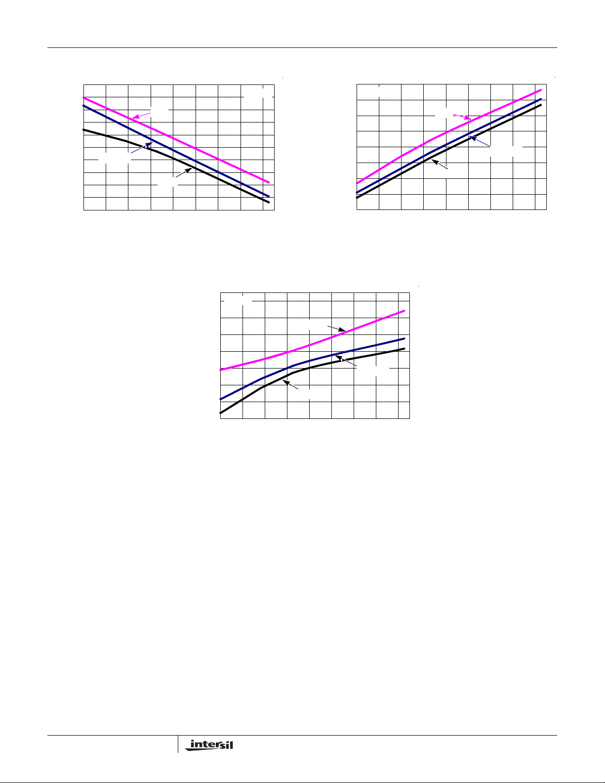
FIGURE 53. PSRR vs TEMPERATURE, V
4.9980
4.9975
4.9970
(V)
4.9965
OUT
IA V
4.9960
4.9955
4.9950
MEDIAN
-40 -20 0 20 40 60 80 100 120
FIGURE 55. IA V
V
+, V-
MIN
MAX
TEMPERATURE (°C)
HIGH vs TEMPERATURE, RL = 100k,
OUT
= ±2.5V
MIN
= +5V, V- = GND, VCM = 1/2V+, TA = +25°C, unless otherwise specified. (Continued)
+
4.910
+, V-
= ±2.5V
n = 100
4.900
4.890
(V)
4.880
OUT
4.870
IA V
4.860
4.850
4.840
FIGURE 54. IA V
(mV)
OUT
IA V
FIGURE 56. IA V
MEDIAN
-40-20 0 20406080100120
OUT
V
= ±2.5V
+, V-
170
n = 100
160
150
140
130
120
110
100
90
-40 -20 0 20 40 60 80 100 120
LOW vs TEMPERATURE, RL = 1k,
OUT
V
= ±2.5V
+, V-
MIN
MAX
TEMPERATURE (°C)
HIGH vs TEMPERATURE, RL = 1k,
MIN
MEDIAN
MAX
TEMPERATURE (°C)
n = 100
6.5
n = 100
6.0
5.5
(mV)
5.0
OUT
IA V
4.5
4.0
3.5
-40 -20 0 20 40 60 80 100 120
FIGURE 57. IA V
V
+, V-
MIN
MAX
TEMPERATURE (°C)
LOW vs TEMPERATURE, RL = 100k,
OUT
= ±2.5V
14
MEDIAN
4.910
4.900
4.890
(V)
4.880
OUT
V
4.870
4.860
4.850
FIGURE 58. V
MEDIAN
-40 -20 0 20 40 60 80 100 120
HIGH vs TEMPERATURE, RL = 1k,
OUT
V
+, V-
MIN
MAX
TEMPERATURE (°C)
= ±2.5V
n = 100
FN6345.2
August 17, 2007
Page 15
ISL28274, ISL28474
Typical Performance Curves V
4.9986
4.9984
4.9982
4.9980
4.9978
(V)
4.9976
OUT
V
4.9974
4.9972
4.9970
4.9968
4.9966
FIGURE 59. V
MEDIAN
-40-200 20406080100120
OUT
V
+, V-
MIN
MAX
TEMPERATURE (°C)
HIGH vs TEMPERATURE, RL = 100k,
= ±2.5V
4.4
4.2
4.0
3.8
(mV)
OUT
3.6
V
3.4
3.2
3.0
FIGURE 61. V
= +5V, V- = GND, VCM = 1/2V+, TA = +25°C, unless otherwise specified. (Continued)
+
170
n = 100
FIGURE 60. V
n = 100
MIN
MAX
-40 -20 0 20 40 60 80 100 120
TEMPERATURE (°C)
LOW vs TEMPERATURE RL = 100k, V
OUT
n = 100
160
150
140
(mV)
130
OUT
V
120
110
100
90
-40 -20 0 20 40 60 80 100 120
LOW vs TEMPERATURE, RL = 1k,
OUT
V
= ±2.5V
+, V-
MEDIAN
= ±2.5V
+, V-
MIN
MEDIAN
MAX
TEMPERATURE (°C)
15
FN6345.2
August 17, 2007
Page 16

ISL28274, ISL28474
Pin Descriptions
ISL28274
(16 LD QSOP)
1, 9, 13, 14
2
3
4
5
6
7
8 18 V- Circuit 4 Negative power supply
10
11
12
15
16 7 V+ Circuit 4 Positive power supply
IA = Instrumentation Amplifier
ISL28474
(24 LD QSOP) PIN NAME
NC No internal connection
11, 14
IA OUT
1, 24
IA OUT_1
IA OUT_2
IA FB+
2, 23
IA FB+_1
IA FB+_2
IA FB-
3, 22
IA FB-_1
IA FB-_2
IA IN-
4, 21
IA IN-_1
IA IN-_2
IA IN+
5, 20
IA IN+_1
IA IN+_2
IA EN
6, 19
IA EN_1
IA EN
_2
EN
8, 17
EN 1
EN
2
IN+
9, 16
IN+ 1
IN+ 2
IN-
10, 15
IN- 1
IN- 2
OUT
12, 13
OUT 1
OUT 2
EQUIVALENT
CIRCUIT DESCRIPTION
Circuit 3 Instrumentation Amplifier output
Circuit 1 Instrumentation Amplifier Feedback from non-inverting output
Circuit 1 Instrumentation Amplifier Feedback from inverting output
Circuit 1 Instrumentation Amplifier inverting input
Circuit 1 Instrumentation Amplifier non-inverting input
Circuit 2 Instrumentation Amplifier enable pin internal pull-down; Logic “1” selects
the disabled state; Logic “0” selects the enabled state.
Circuit 2 Amplifier enable pin with internal pull-down; Logic “1” selects the
disabled state; Logic “0” selects the enabled state.
Circuit 1 Amplifier non-inverting input
Circuit 1 Amplifier inverting input
Circuit 3 Amplifier output
V
+
IN-
CIRCUIT 1
IN+
V
-
LOGIC
PIN
CIRCUIT 2
Description of Operation and Application
Information
Product Description
The ISL28274 and ISL28474 provide both a micropower
instrumentation amplifier (Amp A) and a low power precision
amplifier (Amp B) in the same package. The amplifiers
deliver rail-to-rail input amplification and rail-to-rail output
swing on a single 2.4V to 5V supply. They also deliver
16
V
+
V
-
CIRCUIT 3
V
OUT
V
-
+
V+
V-
CIRCUIT 4
CAPACITIVELY
COUPLED
ESD CLAMP
excellent DC and AC specifications while consuming only
60µA typical supply current per amplifier. Because the
instrumentation amplifiers provide an independent pair of
feedback terminals to set the gain and to adjust the output
level, the in-amp achieves high common-mode rejection
ratio regardless of the tolerance of the gain setting resistors.
The instrumentation amplifier is internally compensated for a
minimum closed loop gain of 100 or greater. An EN
pin is
used to reduce power consumption, typically 4µA for the
FN6345.2
August 17, 2007
Page 17

ISL28274, ISL28474
ISL28274 and 8µA for the ISL28474, while both amplifiers
are disabled. The user has independent control of each
amplifier via separate EN
pins.
Input Protection
The input and feedback terminals have internal ESD
protection diodes to both positive and negative supply rails,
limiting the input voltage to within one diode drop beyond the
supply rails. If overdriving the inputs is necessary, the
external input current must never exceed 5mA. An external
series resistor may be used as a protection to limit excessive
external voltage and current from damaging the inputs.
Input Stage and Input Voltage Range
The input terminals (IN+ and IN-) of both amplifiers “A” and
“B” are single differential pair P-MOSFET devices aided by
an Input Range Enhancement Circuit to increase the
headroom of operation of the common-mode input voltage.
The feedback terminals (FB+ and FB-) of amplifier “A” also
have a similar topology. As a result, the input common-mode
voltage range is rail-to-rail. These amps are able to handle
input voltages that are at or slightly beyond the supply and
ground making them well suited for single 5V or 3.3V low
voltage supply systems. There is no need then to move the
common-mode input to achieve symmetrical input voltage.
Output Stage and Output Voltage Range
A pair of complementary MOSFET devices drives the output
V
to within a few mV of the supply rails. At a 100kΩ load,
OUT
the PMOS sources current and pulls the output up to 4mV
below the positive supply, while the NMOS sinks current and
pulls the output down to 3mV above the negative supply, or
ground in the case of a single supply operation. The current
sinking and sourcing capability of the ISL28274 are internally
limited to 31mA.
Gain Setting of Instrumentation amp “A”
VIN, the potential difference across IN+ and IN-, is replicated
(less the input offset voltage) across FB+ and FB-. The goal
of the ISL28274 in-amp is to maintain the differential voltage
across FB+ and FB- equal to IN+ and IN-; (FB+ - FB-) =
(IN+ - IN-). Consequently, the transfer function can be
derived. The gain is set by two external resistors, the
feedback resistor R
and the gain resistor RG.
F,
2.4V TO 5V
7
VIN/2
VIN/2
VCM
RG
16
V
IN+
6
+
IN-
5
-
FB+
3
+
4
FB-
-
+
ISL28274
V
-
8
RF
EN
FIGURE 62. GAIN IS BY EXTERNAL RESISTORS RF AND R
R
⎛⎞
F
VOUT 1
--------
+
⎜⎟
⎝⎠
VIN=
R
G
In Figure 62, the FB+ pin and one end of resistor R
AMP “A”
2
G
EN
VOUT
G
(EQ. 1)
are
connected to GND. With this configuration, Equation 1 is
only true for a positive swing in VIN; negative input swings
will be ignored and the output will be at ground.
Reference Connection
Unlike a three-op amp instrumentation amplifier, a finite
series resistance seen at the REF terminal does not degrade
the high CMRR performance, eliminating the need for an
additional external buffer amplifier. Figure 63 uses the FB+
pin to provide a high impedance REF terminal.
VCM
2.4V to 5V
REF
VIN/2
VIN/2
R1
R2
RG
6
5
3
4
2.4V TO 5V
IN+
INFB+
FB-
16
V
+
ISL28274
+
-
V
8
RF
7
EN
+
-
AMP “A”
2
EN
VOUT
17
FIGURE 63. GAIN SETTING AND REFERENCE CONNECTION
VOUT 1
R
⎛⎞
F
--------
+
R
VIN()1
G
⎜⎟
⎝⎠
R
⎛⎞
F
--------
+
⎜⎟
⎝⎠
VREF()+=
R
G
(EQ. 2)
The FB+ pin is used as a REF terminal to center or to adjust
the output. Because the FB+ pin is a high impedance input,
an economical resistor divider can be used to set the voltage
at the REF terminal without degrading or affecting the CMRR
performance. Any voltage applied to the REF terminal will
shift V
by resistors R
OUT
by V
times the closed loop gain, which is set
REF
and RG as shown in Figure 63.
F
FN6345.2
August 17, 2007
Page 18

ISL28274, ISL28474
The FB+ pin can also be connected to the other end of resistor,
R
. See Figure 64. Keeping the basic concept that the in-amps
G
maintain constant differential voltage across the input terminals
and feedback terminals (IN+ - IN- = FB+ - FB-), the transfer
function of Figure 64 can be derived.
2.4V TO 5V
7
VIN/2
VIN/2
VCM
RG
VREF
FIGURE 64. REFERENCE CONNECTION WITH AN AVAILABLE
VREF
R
⎛⎞
F
--------
VOUT 1
⎜⎟
⎝⎠
A finite resistance R
output offset of VIN*(R
VIN()VREF()+=
+
R
G
in series with the VREF source, adds an
S
S/RG
16
V
6
IN+
+
5
IN-
-
3
FB+
+
FB-
4
-
+
ISL28274
V
-
8
RF
EN
). As the series resistance RS
AMP “A”
2
EN
VOUT
(EQ. 3)
approaches zero, the gain equation i s simplified to Equa tion 3
for Figure 64. VOUT is simply shifted by an amount VREF.
the in-amp. The proper way to prevent this oscillation is to
short the output to the negative input and ground the positive
input (as shown in Figure 65).
-
+
FIGURE 65. PREVENTING OSCILLATIONS IN UNUSED
CHANNELS
Proper Layout Maximizes Performance
To achieve the maximum performance of the high input
impedance and low offset voltage, care should be taken in
the circuit board layout. The PC board surface must remain
clean and free of moisture to avoid leakage currents
between adjacent traces. Surface coating of the circuit board
will reduce surface moisture and provide a humidity barrier,
reducing parasitic resistance on the board. When input
leakage current is a concern, the use of guard rings around
the amplifier inputs will further reduce leakage currents.
Figure 66 shows a guard ring example for a unity gain
amplifier that uses the low impedance amplifier output at the
same voltage as the high impedance input to eliminate
surface leakage. The guard ring does not need to be a
specific width, but it should form a continuous loop around
both inputs. For further reduction of leakage currents,
components can be mounted to the PC board using PTFE
standoff insulators.
External Resistor Mismatches
Because of the independent pair of feedback terminals
provided by the ISL28274, the CMRR is not degraded by
any resistor mismatches. Hence, unlike a three op amp and
especially a two op amp in-amp, the ISL28274 reduces the
cost of external components by allowing the use of 1% or
more tolerance resistors without sacrificing CMRR
performance. The ISL28274 CMRR will be 100dB
regardless of the tolerance of the resistors used.
Disable/Power-Down
The ISL28274 Amplifiers “A” and “B” can be powered down,
reducing the supply current to typically 4µA. When disabled,
the output is in a high impedance state. The active low EN
bar pin has an internal pull-down and hence, can be left
floating and the in-amp and op amp enabled by default.
When EN
will power down when EN
on when EN
is connected to an external logic, the amplifiers
is pulled above 2V, and will power
is pulled below 0.8V.
Using Only the Instrumentation Amplifier
If the application only requires the instrumentation amp, the
user must configure the unused op amp to prevent it from
oscillating. The unused op amp will oscillate if the input and
output pins are floating. This will result in higher than
expected supply currents and possible noise injection into
HIGH IMPEDANCE INPUT
IN
FIGURE 66. GUARD RING EXAMPLE FOR UNITY GAIN
AMPLIFIER
V+
1/2 ISL28274
1/4 ISL28474
Current Limiting
The ISL28274 has no internal current-limiting circuitry. If the
output is shorted, it is possible to exceed the Absolute
Maximum Rating for output current or power dissipation,
potentially resulting in the destruction of the device.
Power Dissipation
It is possible to exceed the +150°C maximum junction
temperatures under certain load and power-supply
conditions. It is therefore important to calculate the
maximum junction temperature (T
to determine if power supply voltages, load conditions, or
package type need to be modified to remain in the safe
operating area. These parameters are related in Equation 4:
) for all applications
JMAX
18
FN6345.2
August 17, 2007
Page 19

ISL28274, ISL28474
T
JMAXTMAXθJA
xPD
()+=
MAXTOTAL
where:
•PD
MAXTOTAL
is the sum of the maximum power
dissipation of each amplifier in the package (PD
•PD
for each amplifier can be calculated as shown in
MAX
Equation 5:
PD
MAX
2*VSI
( - V
SMAXVS
OUTMAX
)
×+×=
where:
•T
• θ
•PD
•V
•I
•V
= Maximum ambient temperature
MAX
= Thermal resistance of the package
JA
= Maximum power dissipation of 1 amplifier
MAX
= Supply voltage (Magnitude of V+ and V-)
S
= Maximum supply current of 1 amplifier
MAX
OUTMAX
= Maximum output voltage swing of the
application
= Load resistance
•R
L
MAX
V
OUTMAX
----------------------------
R
L
(EQ. 4)
)
(EQ. 5)
19
FN6345.2
August 17, 2007
Page 20

ISL28274, ISL28474
Quarter Size Outline Plastic Packages Family (QSOP)
E E1
0.010 C A B
C
SEATING
PLANE
0.004 C
A
N
1
B
L1
c
SEE DETAI L "X"
D
PIN #1
I.D. MARK
e
0.007 C A B
(N/2)+1
A
(N/2)
MDP0040
QUARTER SIZE OUTLINE PLASTIC PACKAGES FAMILY
INCHES
SYMBOL
A 0.068 0.068 0.068 Max. A1 0.006 0.006 0.006 ±0.002 A2 0.056 0.056 0.056 ±0.004 -
b 0.010 0.010 0.010 ±0.002 -
c 0.008 0.008 0.008 ±0.001 D 0.193 0.341 0.390 ±0.004 1, 3
E 0.236 0.236 0.236 ±0.008 -
H
E1 0.154 0.154 0.154 ±0.004 2, 3
e 0.025 0.025 0.025 Basic -
L 0.025 0.025 0.025 ±0.009 -
b
L1 0.041 0.041 0.041 Basic -
N 16 24 28 Reference -
NOTES:
1. Plastic or metal protrusions of 0.006” maximum per side are not
included.
2. Plastic interlead protrusions of 0.010” maximum per side are not
included.
3. Dimensions “D” and “E1” are measured at Datum Plane “H”.
4. Dimensioning and tolerancing per ASME Y14.5M-1994.
TOLERANCE NOTESQSOP16 QSOP24 QSOP28
Rev. F 2/07
GAUGE
PLANE
L
0.010
4°±4°
A2
A1
DETAIL X
All Intersil U.S. products are manufactured, assembled and tested utilizing ISO9000 quality systems.
Intersil Corporation’s quality certifications can be viewed at www.intersil.com/design/quality
Intersil products are sold by description only. Intersil Corporation reserves the right to make changes in circuit design, software and/or specifications at any time without
notice. Accordingly, the reader is cautioned to verify that data sheets are current before placing orders. Information furnished by Intersil is believed to be accurate and
reliable. However, no responsibility is assumed by Intersil or its subsidiaries for its use; nor for any infringements of patents or other rights of third parties which may result
from its use. No license is granted by implicat ion or oth erwise u nde r any p a tent or p at ent r ights of Intersil or its subsidiaries.
For information regarding Intersil Corporation and its products, see www.intersil.com
20
FN6345.2
August 17, 2007
 Loading...