

®
ISL28271, ISL28272
Data Sheet December 8, 2006
Dual Micropower, Single Supply, Rail-toRail Input and Output (RRIO)
Instrumentation Amplifier
The ISL28271 and ISL28272 are dual micropower
instrumentation amplifiers (in-amps) optimized for low 2.4V
to 5V single supplies.
Both devices feature an Input Range Enhancement Circuit
(IREC) which maintains CMRR performance for input
voltages equal to the positive and negative supply rails. The
input signal is capable of swinging 10% above the positive
supply rail and to 100mV below the negative supply with only
a slight degradation of the CMRR performance. The output
operation is rail to rail.
The ISL28271 is compensated for a minimum gain of 10 or
more. For higher gain applications, the ISL28272 is
compensated for a minimum gain of 100. The in-amps have
CMOS input devices for maximum input common voltage
range. The amplifiers can be operated from one lithium cell
or two Ni-Cd batteries.
FN6390.0
Features
• 120µA typical supply current for both channels
• 30pA max input bias current
• 100dB CMRR, PSRR
• 0.7µV/°C offset voltage temperature coefficient
• 180kHz 3dB Bandwidth - ISL28271
• 100kHz 3dB Bandwidth - ISL28272
• 0.5V/µs slew rate
• Single supply operation
• Rail-to-rail input and output (RRIO)
• Input is capable of swinging above V+ and below V(ground sensing)
• 0.081%1 typical gain error - ISL28271
• -0.19%1 typical gain error - ISL28272
• Pb-free plus anneal available (RoHS compliant)
Ordering Information
PART NUMBER
(Note)
ISL28271FAZ
(Note)
ISL28271FAZ-T7
(Note)
ISL28272FAZ
(Note)
ISL28272FAZ-T7
(Note)
NOTE: Intersil Pb-free plus anneal products employ special Pb-free
material sets; molding compounds/die attach materials and 100% matte
tin plate termination finish, which are RoHS compliant and compatible
with both SnPb and Pb-free soldering operations. Intersil Pb-free
products are MSL classified at Pb-free peak reflow temperatures that
meet or exceed the Pb-free requirements of IPC/JEDEC J STD-020.
PART
MARKING
28271 FAZ 97/Tube 16 Ld QSOP
28271 FAZ 7”
28272 FAZ 97/Tube 16 Ld QSOP
28272 FAZ 7”
TAPE &
REEL
(1000 pcs)
(1000 pcs)
PACKAGE
(Pb-Free)
(Pb-free)
16 Ld QSOP
(Pb-free)
(Pb-free)
16 Ld QSOP
(Pb-free)
PKG.
DWG. #
MDP0040
MDP0040
MDP0040
MDP0040
Applications
• Battery- or solar-powered systems
• Strain gauge
• Sensor signal conditioning
• Medical devices
• Industrial instrumentations
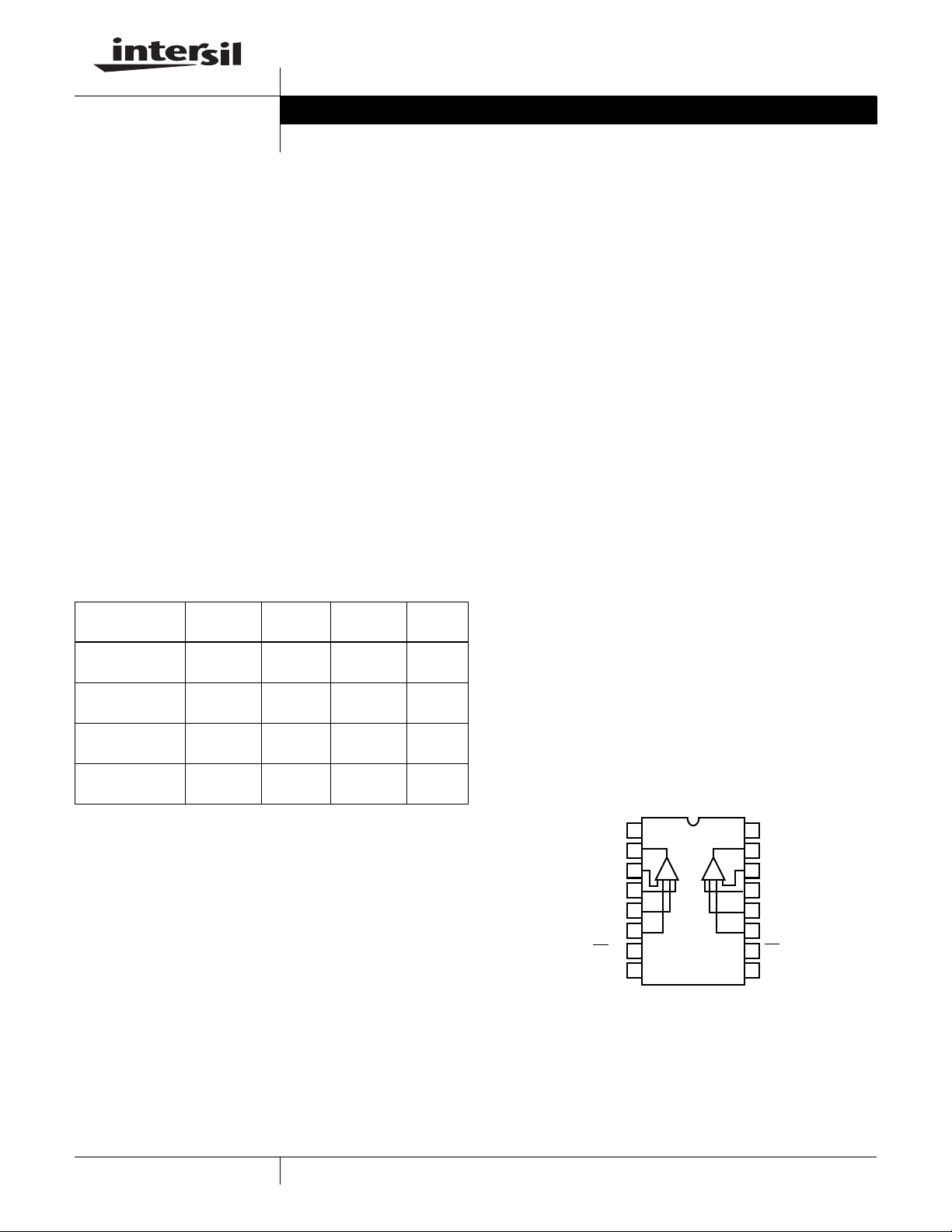
Pinout
ISL28271, ISL28272
(16 LD QSOP)
TOP VIEW
NC
1
2
OUT_A
3
FB+_A
FB-_A
IN-_A
IN+_A
EN
_A
4
5
6
7
V-
8
-+-+
16
15
14
13
12
11
10
9
V+
OUT_B
FB+_B
FB-_B
IN-_B
IN+_B
EN
_B
NC
1
CAUTION: These devices are sensitive to electrostatic discharge; follow proper IC Handling Procedures.
1-888-INTERSIL or 1-888-468-3774
| Intersil (and design) is a registered trademark of Intersil Americas Inc.
All other trademarks mentioned are the property of their respective owners.
Copyright © Intersil Americas Inc. 2006. All Rights Reserved.
ISL28271, ISL28272
Absolute Maximum Ratings (T
Supply Voltage. . . . . . . . . . . . . . . . . . . . . . . . . . . . . . . . . . . . . . 5.5V
Supply Turn On Voltage Slew Rate . . . . . . . . . . . . . . . . . . . . . 1V/μs
Input Current (IN, FB) ISL28272 . . . . . . . . . . . . . . . . . . . . . . . . 5mA
Differential Input Voltage (IN, FB) ISL28272 . . . . . . . . . . . . . . . 0.5V
Input Current (IN, FB) ISL28271 . . . . . . . . . . . . . . . . . . . . . . . . 5mA
Differential Input (IN, FB) Voltage ISL28271 . . . . . . . . . . . . . . . 1.0V
Input Voltage . . . . . . . . . . . . . . . . . . . . . . . . . V-
ESD tolerance, Human Body Model . . . . . . . . . . . . . . . . . . . . . .3kV
= +25°C) Thermal Information
A
Thermal Resistance θ
16 Ld QSOP Package . . . . . . . . . . . . . . . . . . . . . . . 112
Output Short-Circuit Duration . . . . . . . . . . . . . . . . . . . . . . .Indefinite
Ambient Operating Temperature Range . . . . . . . . .-40°C to +125°C
Storage Temperature Range . . . . . . . . . . . . . . . . . .-65°C to +150°C
Operating Junction Temperature . . . . . . . . . . . . . . . . . . . . . +125°C
- 0.5V to V+ + 0.5V
(°C/W)
JA
ESD tolerance, Machine Model . . . . . . . . . . . . . . . . . . . . . . . . .300V
CAUTION: Stresses above those listed in “Absolute Maximum Ratings” may cause permanent damage to the device. This is a stress only rating and operation of the
device at these or any other conditions above those indicated in the operational sections of this specification is not implied .
IMPORTANT NOTE: All parameters having Min/Max specifications are guaranteed. Typical values are for information purposes only. Unless otherwise noted, all tests
are at the specified temperature and are pulsed tests, therefore: TJ = TC = T
Electrical Specifications V+ = +5V, V- = GND, V
operating temperature range, -40°C to +125°C.
A
= 1/2V+, TA = +25°C, unless otherwise specified. Boldface limits apply over the
FB+
PARAMETER DESCRIPTION CONDITIONS MIN TYP MAX UNIT
V
TCV
I
OS
I
e
OS
B
N
OS
Input Offset Voltage ISL28271 -600
-1200
ISL28272 -500
-750
Input Offset Voltage Temperature
Coefficient -40°C to +125°C
Input Offset Current between IN+ and
IN-, and between FB+ and FB-
Input Bias Current (IN+, IN-, FB+, and
FB- terminals)
See graphs for extended temperature range
-40°C to +85°C
See graphs for extended temperature range
-40°C to +85°C
-30
-80
-30
-80
Input Noise Voltage ISL28271 f = 0.1Hz to 10Hz 10 µV
ISL28272 6 µV
±35
600
µV
1200
±35 500
µV
750
0.7 µV/°C
±5 30
pA
80
±10 30
pA
80
P-P
P-P
Input Noise Voltage Density ISL28271 fo = 1kHz 240 nV/√Hz
ISL28272 78 nV/√Hz
i
N
Input Noise Current Density ISL28271 fo = 1kHz 0.92 pA/√Hz
ISL28272 0.2 pA/√Hz
R
IN
V
IN
CMRR Common Mode Rejection Ratio ISL28271 V
Input Resistance 1GΩ
Input Voltage Range V+ = 2.4V to 5.0V 0 V+ V
= 0V to 5V 80
CM
70
ISL28272 80
100 dB
100 dB
75
PSRR Power Supply Rejection Ratio V+ = 2.4V to 5V 80
100 dB
75
E
G
Gain Error ISL28271 RL = 100kΩ to 2.5V +0.081 %
ISL28272 -0.19
2
FN6390.0
December 8, 2006
ISL28271, ISL28272
Electrical Specifications V+ = +5V, V- = GND, V
operating temperature range, -40°C to +125°C. (Continued)
= 1/2V+, TA = +25°C, unless otherwise specified. Boldface limits apply over the
FB+
PARAMETER DESCRIPTION CONDITIONS MIN TYP MAX UNIT
V
OUT
Maximum Voltage Swing Output low, RL = 100kΩ 3630mV
Output low, R
= 1kΩ 130 175
L
225
Output high, R
Output high, R
SR Slew Rate R
-3db BW -3dB Bandwidth R
= 1kΩ to GND 0.4
L
= 10kΩ ISL28271 180 kHz
L
= 100kΩ 4.980
L
= 1kΩ 4.85
L
4.980
4.80
0.35
4.99 V
4.88 V
0.5 0.7
0.75
ISL28272 100 kHz
I
S,EN
I
S,DIS
Supply Current, Enabled Both A and B channels enabled, EN = V- 120 156
200
Supply Current, Disabled Both A and B channels disabled, EN =V+ 4 7
9
V
V
I
ENH
INH
INL
EN Enable Pin High Level 2 V
EN Enable Pin Low Level 0.8 V
EN Input Current High EN = V+ 0.8 1
1.3
I
ENL
EN Input Current Low EN = V- 26 50
100
V+ Minimum Supply Voltage 2.4 V
I
SC+
I
SC-
Short Circuit Output Current V+ = 5V, RL = 10Ω 28
25
Short Circuit Output Current V+ = 5V, RL = 10Ω 24
20
31 mA
26 mA
mV
V/µs
µA
µA
µA
nA
3
FN6390.0
December 8, 2006
Typical Performance Curves
ISL28271, ISL28272
70
60
50
40
GAIN (dB)
30
20
10
1 10 100 1k 10k 100k 1M
GAIN = 1000
GAIN = 500
GAIN = 200
GAIN = 100
GAIN = 50
GAIN = 20
GAIN = 10
FREQUENCY (Hz)
VCM = 5V
V
= 10mV
OUT
RL = 10k
PP
FIGURE 1. ISL28271 FREQUENCY RESPONSE vs CLOSED
LOOP GAIN. V+ = V
70
60
50
40
GAIN (dB)
30
20
GAIN = 1000
GAIN = 500
GAIN = 200
GAIN = 100
GAIN = 50
GAIN = 20
GAIN = 10
CM
= 5V
VCM = 2.5V
= 10mV
V
OUT
RL = 10k
PP
90
80
70
60
GAIN (dB)
50
40
30
GAIN = 10,000
GAIN = 5,000
GAIN = 2,000
GAIN = 1,000
GAIN = 500
GAIN = 200
GAIN = 100
1 10 100 1k 10k 100k 1M
FREQUENCY (Hz)
VCM = 5V
= 10mV
V
OUT
RL = 10k
PP
FIGURE 2. ISL28272 FREQUENCY RESPONSE vs CLOSED
LOOP GAIN. V
90
80
70
60
GAIN (dB)
50
40
GAIN = 10,000
GAIN = 5,000
GAIN = 2,000
GAIN = 1,000
GAIN = 500
GAIN = 200
GAIN = 100
CM
= V+
VCM = 2.5V
= 10mV
V
OUT
RL = 10k
PP
10
1 10 100 1k 10k 100k 1M
FREQUENCY (Hz)
FIGURE 3. ISL28271 FREQUENCY RESPONSE vs CLOSED
LOOP GAIN. V+ = 5V, V
70
60
50
40
GAIN (dB)
30
20
10
1 10 100 1k 10k 100k 1M
GAIN = 1000
GAIN = 500
GAIN = 200
GAIN = 100
GAIN = 50
GAIN = 20
GAIN = 10
FREQUENCY (Hz)
CM
= 1/2V+
VCM = +10mV
V
= 10mV
OUT
RL = 10k
PP
FIGURE 5. ISL28271 FREQUENCY RESPONSE vs CLOSED
LOOP GAIN. V+ = 5V, V
CM
= 10mV
30
1 10 100 1k 10k 100k 1M
FREQUENCY (Hz)
FIGURE 4. ISL28272 FREQUENCY RESPONSE vs CLOSED
LOOP GAIN. V
90
80
70
60
GAIN (dB)
50
40
30
GAIN = 10,000
GAIN = 5,000
GAIN = 2,000
GAIN = 1,000
GAIN = 500
GAIN = 200
GAIN = 100
1 10 100 1k 10k 100k 1M
= 1/2V+
CM
FREQUENCY (Hz)
VCM = +10mV
V
= 10mV
OUT
RL = 10k
PP
FIGURE 6. ISL28272 FREQUENCY RESPONSE vs CLOSED
LOOP GAIN. V
CM
= V-
4
FN6390.0
December 8, 2006
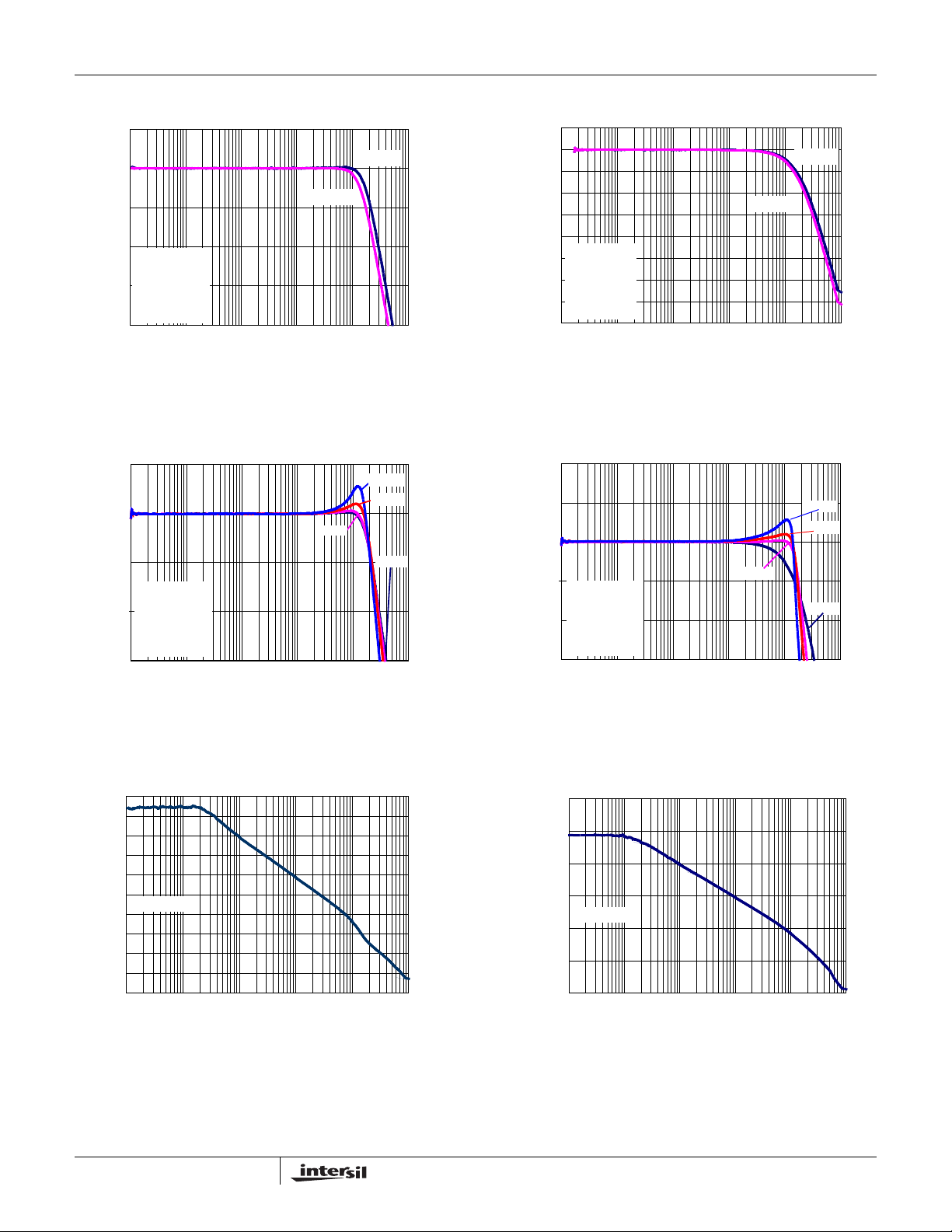
Typical Performance Curves (Continued)
25
= 2.4V
S
VS = 5V
20
15
10
GAIN (dB)
AV = 10
= 10kΩ
R
L
= 10pF
C
L
5
R
= 10
F/RG
= 1kΩ
R
F
= 100Ω
R
G
0
10
100 10k1k 100k 1M
FREQUENCY (Hz)
V
ISL28271, ISL28272
45
40
35
30
25
20
GAIN (dB)
15
10
5
0
AV = 100
= 10kΩ
R
L
= 10pF
C
L
R
F/RG
= 10kΩ
R
F
= 100Ω
R
G
10
VS = 5V
V
= 2.4V
S
= 100
100 10k1k 100k 1M
FREQUENCY (Hz)
FIGURE 7. ISL28271 FREQUENCY RESPONSE vs SUPPLY
VOLTAGE
25
820pF
20
220pF
15
GAIN (dB)
AV = 10
= 10kΩ
R
10
C
= 10pF
L
= 10
R
F/RG
= 1kΩ
R
F
R
= 100Ω
G
5
10
100 10k1k 100k 1M
FREQUENCY (Hz)
FIGURE 9. ISL28271 FREQUENCY RESPONSE vs C
90
80
70
60
50
40
AV = 10
30
CMRR (dB)
20
10
0
-10
10 100 1k 10k 100k 1M
FREQUENCY (Hz)
470pF
100pF
LOAD
FIGURE 11. ISL28271 CMRR vs FREQUENCY
FIGURE 8. ISL28272 FREQUENCY RESPONSE vs SUPPLY
VOLTAGE
50
45
40
35
GAIN (dB)
30
25
AV = 100
= 10kΩ
R
C
= 10pF
L
R
F/RG
= 10kΩ
R
F
= 100Ω
R
G
10
= 100
100 10k1k 100k 1M
FREQUENCY (Hz)
820pF
FIGURE 10. ISL28272 FREQUENCY RESPONSE vs C
120
100
80
60
CMRR (dB)
AV = 100
40
20
0
10 100 1k 10k 100k
FREQUENCY (Hz)
2200pF
1200pF
56pF
LOAD
1M
FIGURE 12. ISL28272 CMRR vs FREQUENCY
5
FN6390.0
December 8, 2006

Typical Performance Curves (Continued)
120
ISL28271, ISL28272
120
100
80
60
PSRR (dB)
40
AV = 10
20
0
10 100 1k 10k 100k 1M
PSRR-
FREQUENCY (Hz)
PSRR+
100
80
60
PSRR (dB)
40
AV = 100
20
0
10 100 1k 10k 100k 1M
PSRR-
FREQUENCY (Hz)
FIGURE 13. ISL28271 PSRR vs FREQUENCY FIGURE 14. ISL28272 PSRR vs FREQUENCY
1400
1200
1000
800
600
400
200
INPUT VOLTAGE NOISE (nV/√Hz)
0
1 10 100 1k 10k 100k
AV = 10
FREQUENCY (Hz)
FIGURE 15. ISL28271 INPUT VOLT AGE NOISE SPECTRAL
DENSITY
700
600
500
400
300
200
100
INPUT VOLTAGE NOISE (nV/√Hz)
0
1 10 100 1k 10k 100k
AV = 100
FREQUENCY (Hz)
FIGURE 16. ISL28272 INPUT VOLT AGE NOISE SPECTRAL
DENSITY
PSRR+
6
5
4
3
2
1
CURRENT NOISE (pA/√Hz)
0
1 10 100 1k 10k 100k
AV = 10
FREQUENCY (Hz)
FIGURE 17. ISL28271 INPUT CURRENT NOISE SPECTRAL
DENSITY
6
2.0
1.8
1.6
1.4
1.2
1.0
0.8
0.6
0.4
CURRENT NOISE (pA/√Hz)
0.2
0.0
1 10 100 1k
AV = 100
10k
FREQUENCY (Hz)
FIGURE 18. ISL28272 INPUT CURRENT NOISE SPECTRAL
DENSITY
FN6390.0
December 8, 2006
100k

Typical Performance Curves (Continued)
ISL28271, ISL28272
VOLTAGE NOISE (5µV/DIV)
TIME (1s/DIV)
FIGURE 19. ISL28271 0.1 Hz TO 10Hz INPUT VOLTAGE NOISE.
GAIN = 10
n = 3000
190
170
150
MEDIAN
130
110
90
SUPPLY CURRENT (µA)
70
50
-40 -20 0 20 40 60 80 100 120
MAX
MIN
TEMPERATURE (°C)
FIGURE 21. ISL28271 SUPPLY CURRENT ENABLED vs
TEMPERATURE V
= ±2.5V, VIN = 0V
S
VOLTAGE NOISE (2µV/DIV)
TIME (1s/DIV)
FIGURE 20. ISL28272 0.1 Hz TO 10Hz INPUT VOLTAGE NOISE.
GAIN = 100
160
n = 3000
150
140
130
MEDIAN
120
110
SUPPLY CURRENT (µA)
100
90
-40 -20 0 20 40 60 80 100 120
TEMPERATURE (°C)
MAX
MIN
FIGURE 22. ISL28272 SUPPLY CURRENT ENABLED vs
TEMPERATURE V
= ±2.5V, VIN = 0V
S
5.0
n = 3000
4.5
4.0
3.5
SUPPL Y CURRENT (µA)
3.0
2.5
-40-200 20406080100120
MAX
MEDIAN
MIN
TEMPERATURE (°C)
FIGURE 23. ISL28271 SUPPLY CURRENT DISABLED vs
TEMPERATURE V
= ±2.5V, VIN = 0V
S
7
7
n = 3000
6
5
4
3
MEDIAN
2
SUPPLY CURRENT (µA)
1
0
-40-200 20406080100120
MAX
MIN
TEMPERATURE (°C)
FIGURE 24. ISL28272 SUPPLY CURRENT DISABLED vs
TEMPERATURE V
= ±2.5V, VIN = 0V
S
December 8, 2006
FN6390.0

Typical Performance Curves (Continued)
ISL28271, ISL28272
160
n = 3000
150
140
130
120
110
CMRR (dB)
100
90
80
70
-40 -20 0 20 40 60 80 100 120
MEDIAN
TEMPERATURE (°C)
MAX
MIN
FIGURE 25. ISL28271 CMRR vs TEMPERATURE VCM= +2.5V
TO -2.5V
150
140
130
120
110
100
PSRR (dB)
90
80
70
60
-40 -20 0 20 40 60 80 100 120
MAX
MEDIAN
MIN
TEMPERATURE (°C)
FIGURE 27. ISL28271 PSRR vs TEMPERATURE V
±2.5V
n = 3000
= ±1.2V TO
S
190
n = 3000
170
150
130
CMRR (dB)
110
90
70
MEDIAN
-40 -20 0 20 40 60 80 100 120
TEMPERATURE (°C)
MAX
MIN
FIGURE 26. ISL28272 CMRR vs TEMPERATURE VCM= +2.5V
TO -2.5V
180
n = 3000
160
140
120
PSRR (dB)
100
80
60
-40 -20 0 20 40 60 80 100 120
MEDIAN
MIN
TEMPERATURE (°C)
FIGURE 28. ISL28272 PSRR vs TEMPERATURE V
±2.5V
MAX
= ±1.2V TO
S
4.91
4.90
4.89
4.88
(V)
OUT
4.87
V
4.86
4.85
4.84
-40 -20 0 20 40 60 80 100 120
FIGURE 29. ISL28271 V
V
= ±2.5V
S
MEDIAN
TEMPERATURE (°C)
OUT
HIGH vs TEMPERATURE RL= 1k,
MAX
MIN
8
n = 3000
4.91
4.90
4.89
4.88
(V)
OUT
4.87
V
4.86
4.85
4.84
MEDIAN
FIGURE 30. ISL28272 V
V
= ±2.5V
S
n = 3000
MAX
MIN
TEMPERATURE (°C)
HIGH vs TEMPERATURE RL= 1k,
OUT
December 8, 2006
120-40 -20 0 20 40 60 80 100
FN6390.0

Typical Performance Curves (Continued)
ISL28271, ISL28272
4.9980
n = 3000
4.9975
4.9970
(V)
4.9965
OUT
V
4.9960
4.9955
4.9950
-40 -20 0 20 40 60 80 100 120
FIGURE 31. ISL28271 V
170
n = 3000
160
150
140
(mV)
130
OUT
120
V
110
100
90
-40 -20 0 20 40 60 80 100 120
FIGURE 33. ISL28271 V
100k, V
V
= ±2.5V
S
MEDIAN
MIN
TEMPERATURE (°C)
HIGH vs TEMPERATURE RL =
OUT
= ±2.5V
S
MIN
TEMPERATURE (°C)
LOW vs TEMPERATURE RL = 1k,
OUT
MAX
MAX
MEDIAN
4.998
4.9975
4.997
(V)
4.9965
OUT
V
4.996
4.9955
4.995
FIGURE 32. ISL28272 V
(mV)
OUT
V
FIGURE 34. ISL28272 V
n = 3000
MEDIAN
MAX
MIN
-40 -20 0 20 40 60 80 100 120
TEMPERATURE (°C)
HIGH vs TEMPERATURE RL=
OUT
= ±2.5V
S
MAX
MEDIAN
MIN
TEMPERATURE (°C)
LOW vs TEMPERA TURE RL=1k,
OUT
180
170
160
150
140
130
120
110
100
90
80
100k, V
n = 3000
V
S
= ±2.5V
120-40 -20 0 20 40 60 80 100
6.0
n = 3000
5.8
5.6
5.4
5.2
(mV)
5.0
OUT
4.8
V
4.6
4.4
4.2
4.0
-40-200 20406080100120
FIGURE 35. ISL28271 V
R
= 100k, VS = ±2.5V
L
MEDIAN
TEMPERATURE (°C)
LOW vs TEMPERATURE
OUT
MAX
MIN
9
6
n = 3000
5.8
5.6
5.4
5.2
(mV)
5
OUT
4.8
V
4.6
4.4
4.2
4
-40 -20 0 20 40 60 80 100 120
FIGURE 36. ISL28272 V
R
= 100k, VS = ±2.5V
L
MEDIAN
TEMPERATURE (°C)
LOW vs TEMPERATURE
OUT
MAX
MIN
FN6390.0
December 8, 2006

Pin Descriptions
ISL28271, ISL28272
ISL28271
16 Ld QSOP
ISL28272
16 Ld QSOP PIN NAME
EQUIVALENT
CIRCUIT PIN FUNCTION
2, 15 2, 15 OUT_A,B Circuit 3 Output Voltage. A complementary Class AB common-source output stage drives
the output of each channel. When disabled, the outputs are in a high impedance
state.
3, 14 3, 14 FB+_A,B Circuit 1A,
Circuit 1B
Positive Feedback high impedance terminals. ISL28272 input circuit is shown in
Circuit 1A, and the ISL28271 input circuit is shown in Circuit 1B.
ISL28271: to avoid offset drift, it is recommended that the terminals of the
ISL28271 are not overdriven beyond 1V and the input current must never
exceed 5mA.
4, 13 4, 13 FB-_A,B Circuit 1A,
Circuit 1B
Negative Feedback high impedance terminals. The FB- pins connect to an
external resistor divider to individually set the desired gain of the in-amp.
ISL28272 input circuit is shown in Circuit 1A, and the ISL28271 input circuit is
shown in Circuit 1B.
ISL28271: to avoid offset drift, it is recommended that the terminals of the
ISL28271 are not overdriven beyond 1V and the input current must never
exceed 5mA.
5, 12 5, 12 IN-_A,B Circuit 1A,
Circuit 1B
High impedance Inverting input terminals. Connect to the low side of the input
source signal. ISL28272 input circuit is shown in Circuit 1A, and the ISL28271
input circuit is shown in Circuit 1B.
ISL28271: to avoid offset drift, it is recommended that the terminals of the
ISL28271 are not overdriven beyond 1V and the input current must never
exceed 5mA.
6, 11 6, 11 IN+_A,B Circuit 1A,
Circuit 1B
High impedance Non-inverting input terminals. Connect to the high side of the
input source signal. ISL28272 input circuit is shown in Circuit 1A, and the
ISL28271 input circuit is shown in Circuit 1B.
ISL28271: to avoid offset drift, it is recommended that the terminals of the
ISL28271 are not overdriven beyond 1V and the input current must never
exceed 5mA.
7, 10 7, 10 EN
_A,B Circuit 2 Active LOW logic pins. When pulled above 2V, the corresponding channel turns
off and OUT is high impedance. A channel is enabled when pulled below 0.8V.
Built-in pull downs define each EN
pin LOW when left floating.
16 16 V+ Circuit 4 Positive Supply terminal shared by all channels.
8 8 V- Circuit 4 Negative Supply terminal shared by all channels. Grounded for single supply
operation.
1, 9 1, 9 NC No Connect, pins can be left floating or grounded.
IN-
FB-
IN-
FB-
CIRCUIT 1A
CIRCUIT 1B
V+
IN+
FB+
V-
10
V+
IN+
FB+
V-
LOGIC
PIN
CIRCUIT 2
V+
V-
CIRCUIT 3
V+
OUT
V-
V+
V-
CIRCUIT 4
CAPACITIVELY
COUPLED
ESD CLAMP
December 8, 2006
FN6390.0
ISL28271, ISL28272
Application Information
Product Description
The ISL28271 and ISL28272 are dual channel micropower
instrumentation amplifiers (in-amps) which deliver rail-to-rail
input amplification and rail-to-rail output swing. The in-amps
also deliver excellent DC and AC specifications while
consuming only about 120µA for both channels. Because
the independent pair of feedback terminals set the gain and
adjust the output zero level, the ISL28271 and ISL28272
achieve high CMRR regardless of the tolerance of the gain
setting resistors. The ISL28271 is internally compensated for
a minimum gain of 10. The ISL28272 is internally
compensated for a minimum gain of 100.
EN
pins are available to independently enable or disable a
channel. When all channels are off, current consumption is
down to typically 4µA.
Input Protection
All input terminals and feedback terminals have internal ESD
protection diodes to both positive and negative supply rails,
limiting the input voltage to within one diode beyond the
supply rails. Input signals originating from low impedance
sources should have current limiting resistors in series with
the IN+ and IN- pins to prevent damaging currents during
power supply sequencing and other transient conditions.
The ISL28272 has additional back-to-back diodes across the
input terminals and also across the feedback terminals. If
overdriving the inputs is necessary, the external input current
must never exceed 5mA. External series resistors may be
used as an external protection to limit excessive external
voltage and current from damaging the inputs. On the other
hand, the ISL28271 has no clamps to limit the differential
voltage on the input terminals allowing higher differential
input voltages at lower gain applications. It is recommended
however, that the terminals of the ISL28271 are not
overdriven beyond 1V to avoid offset drift.
performance charts. IREC also cures the abrupt change and
even reverse polarity of the input bias current over the whole
range of input.
Output Stage and Output Voltage Range
A Class AB common-source output stage drives the output.
The pair of complementary MOSFET devices drive the
output VOUT to within a few millivolts of the supply rails. At a
100kΩ load, the PMOS sources current and pulls the output
up to 4mV below the positive supply. The NMOS sinks
current and pulls the output down to 4mV above the negative
supply, or ground in the case of a single supply operation.
The current sinking and sourcing capability are internally
limited to 31mA. When disabled, the outputs are in a high
impedance state.
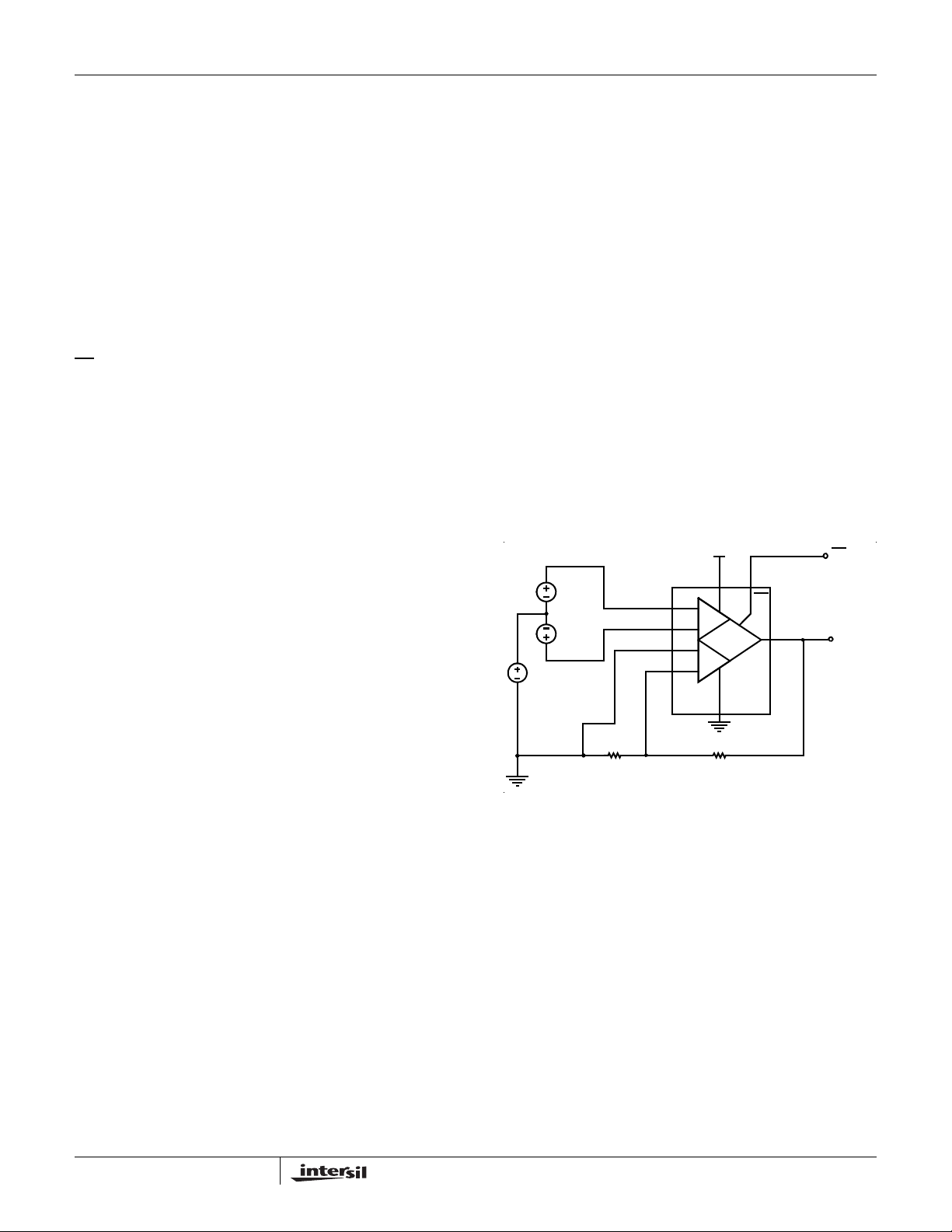
Gain Setting
VIN, the potential difference across IN+ and IN-, is replicated
(less the input offset voltage) across FB+ and FB-. The
function of the in-amp is to maintain the differential voltage
across FB- and FB+ equal to IN+ and IN-; (FB- - FB+) =
(IN+ - IN-). Consequently, the transfer function can be
derived. The in-amp gain is set by two external resistors, the
feedback resistor RF, and the gain resistor RG.
VCM
IN+
IN-
2.4V to 5V
IN+
INFB+
FB-
+
-
+
-
V+
V-
ISL28271
ISL28272
RFRG
EN
EN
VOUT
Input Stage and Input Voltage Range
The input terminals (IN+ and IN-) of the in-amps are a single
differential pair of CMOS devices aided by an Input Range
Enhancement Circuit, IREC, to increase the headroom of
operation of the common-mode input voltage. The feedback
terminals (FB+ and FB-) also have a similar topology. As a
result, the input common-mode voltage range is rail-to-rail
regardless of the feedback terminal settings and regardless
of the gain settings. They are able to handle input voltages
that are at or slightly beyond the supply and ground sensing
making these in-amps well suited for single 5V down to 2.4V
supply systems.
The IREC enables rail-to-rail input amplification without the
problems usually associated with the dual differential stage
topology. The IREC ensures that there are no drastic
changes in offset voltage over the entire range of the input.
See Input Offset Voltage vs Common-Mode Input Voltage in
11
FIGURE 37. GAIN IS SET BY TWO EXTERNAL RESISTORS,
R
AND R
VIN IN+ IN-–=
VOUT 1
⎛⎞
⎜⎟
⎝⎠
F
R
--------
+
R
G
G
F
VIN=
(EQ. 1)
In Figure 37, the FB+ pin and one end of resistor RG are
connected to GND. With this configuration, the above gain
equation (Equation 1) is only true for a positive sw ing in VIN ;
negative input swings will be ignored because the output will
be at ground.
Reference Connection
Unlike a three op-amp in-amp realization, a finite series
resistance seen at the REF terminal does not degrade the
high CMRR performance eliminating the need for an
FN6390.0
December 8, 2006

ISL28271, ISL28272
additional external buffer amplifier. Figure 38 uses the FB+
pin to provide a high impedance REF terminal.
2.4V to 5V
VCM
IN+
IN-
2.9V to 5V
R1
REF
R2
IN+
INFB+
FB-
V+
+
ISL28271
+
-
ISL28271
ISL28272
RFRG
EN
V-
FIGURE 38. GAIN SETTING AND REFERENCE CONNECTION
.
VIN IN+ IN-–=
VOUT 1
⎛⎞
⎜⎟
⎝⎠
+
R
--------
R
F
VIN()1
G
R
⎛⎞
F
--------
+
⎜⎟
⎝⎠
VREF()+=
R
G
EN
VOUT
(EQ. 2)
The FB+ pin is used as a REF terminal to center or to adjust
the output. Because the FB+ pin is a high impedance input,
an economical resistor divider can be used to set the voltage
at the REF terminal without degrading or affecting the CMRR
performance. Any voltage applied to the REF terminal will
shift VOUT by VREF times the closed loop gain, which is set
by resistors RF and RG. See Figure 38.
The FB+ pin can also be connected to the other end of
resistor, RG. See Figure 39. Keeping the basic concept that
the in-amp maintains constant dif ferential volt ag e across the
input terminals and feedback terminals (FB- - FB+) =
(IN+ - IN-), the transfer function of Figure 39 can be derived.
2.4V to 5V
IN+
IN-
VCM
RS
VREF
IN+
INFB+
FB-
V+
+
ISL28271
+
-
ISL28271
ISL28272
RFRG
EN
V-
FIGURE 39. REFERENCE CONNECTION WITH AN
AVAILABLE VREF
EN
VOUT
VIN IN+ IN-–=
+
R
SRF
--------------------- -
VOUT 1
VOUT 1
+ VREF+=
R
G
R
⎛⎞
F
--------
+
⎜⎟
⎝⎠
VIN()VREF()+=
R
G
(EQ. 3)
(EQ. 4)
A finite resistance RS in series with the VREF source, adds
an output offset of VIN*(RS/RG). As the series resistance
RS approaches zero, Equation 3 is simplified to Equation 4
for Figure 39. VOUT is simply shifted by an amount VREF.
External Resistor Mismatches
Because of the independent pair of feedback terminals
provided by the in-amps, the CMRR is not degraded by any
resistor mismatches. Hence, unlike a three op-amp and
especially a two op-amp in-amp realization, the ISL28271
and ISL28272 reduce the cost of external components by
allowing the use of 1% or more tolerance resistors without
sacrificing CMRR performance. The CMRR will be typically
110dB regardless of the tolerance of the resistors used.
Instead, a resistor mismatch results in a higher deviation
from the theoretical gain - Gain Error.
Gain Error and Accuracy
The gain error indicated in the electrical specifications table
is the inherent gain error alone. The gain error specification
listed does not include the gain error contributed by the
resistors. There is an additional gain error due to the
tolerance of the resistors used. The resulting non-ideal
transfer function effectively becomes:
VOUT 1
⎜⎟
⎝⎠
--------
+
1E
R
G
++()±[]VIN××=
RGERFEG
(EQ. 5)
R
⎛⎞
F
Where:
ERG = Tolerance of RG
ERF = Tolerance of RF
EG = Gain Error of the ISL28271
The term [1 - (ERG +ERF +EG)] is the deviation from the
theoretical gain. Thus, (ERG +ERF +EG) is the total gain
error. For exa mp l e, if 1% resistors are used, the total gain
error would be:
TotalGainError E
TotalGainError 0.01 0.01 0.005++()2.5%±=±=
RGERFEG
typical()++()±=
Disable/Power-Down
The ISL28271 and ISL28272 have an enable/disable pin for
each channel. They can be powered down to reduce the
supply current to typically 4µA when all channels are off.
When disabled, the corresponding output is in a high
impedance state. The active low
down and hence can be left floating and the in-amp enabled
by default. When the
EN is connected to an external logic,
EN pin has an internal pull
12
FN6390.0
December 8, 2006

ISL28271, ISL28272
the in-amp will shutdown when EN pin is pulled above 2V,
and will power up when
Unused Channels
The ISL28271and ISL28272 are Dual channel op-amps. If
the application only requires one channel when using the
ISL28271 or ISL28272, the user must configure the unused
channel to prevent it from oscillating. The unused channel
will oscillate if the input and output pins are floating. This will
result in higher than expected supply currents and possible
noise injection into the channel being used. The proper wa y
to prevent this oscillation is to configure the feedback pins
(FB+, FB-) with the minimum gain stable values for the
amplifier with RF and RG resistors and tieing the input
terminals to ground (as shown in Figure 40).
EN bar is pulled below 0.8V.
IN+
+
IN-
-
FB+
+
FB-
-
RG
FIGURE 40. PREVENTING OSCILLATIONS IN UNUSED
CHANNELS
RF
13
FN6390.0
December 8, 2006
ISL28271, ISL28272
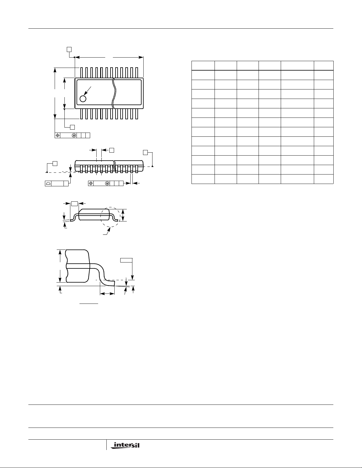
Quarter Size Outline Plastic Packages Family (QSOP)
E E1
0.010 C A B
C
SEATING
PLANE
0.004 C
A
N
1
B
L1
c
SEE DETAI L "X"
D
PIN #1
I.D. MARK
e
0.007 C A B
(N/2)+1
A
(N/2)
MDP0040
QUARTER SIZE OUTLINE PLASTIC PACKAGES FAMILY
SYMBOL QSOP16 QSOP24 QSOP28 TOLERANCE NOTES
A 0.068 0.068 0.068 Max. A1 0.006 0.006 0.006 ±0.002 A2 0.056 0.056 0.056 ±0.004 -
b 0.010 0.010 0.010 ±0.002 -
c 0.008 0.008 0.008 ±0.001 -
D 0.193 0.341 0.390 ±0.004 1, 3
E 0.236 0.236 0.236 ±0.008 -
E1 0.154 0.154 0.154 ±0.004 2, 3
H
b
e 0.025 0.025 0.025 Basic L 0.025 0.025 0.025 ±0.009 -
L1 0.041 0.041 0.041 Basic -
N 16 24 28 Reference -
Rev. E 3/01
NOTES:
1. Plastic or metal protrusions of 0.006” maximum per side are not
included.
2. Plastic interlead protrusions of 0.010” maximum per side are not
included.
3. Dimensions “D” and “E1” are measured at Datum Plane “H”.
4. Dimensioning and tolerancing per ASME Y14.5M-1994.
GAUGE
PLANE
L
0.010
4°±4°
A2
A1
DETAIL X
All Intersil U.S. products are manufactured, assembled and tested utilizing ISO9000 quality systems.
Intersil Corporation’s quality certifications can be viewed at www.intersil.com/design/quality
Intersil products are sold by description only. Intersil Corporation reserves the right to make changes in circuit design, software and/or specifications at any time without
notice. Accordingly, the reader is cautioned to verify that data sheets are current before placing orders. Information furnished by Intersil is believed to be accurate and
reliable. However, no responsibility is assumed by Intersil or its subsidiaries for its use; nor for any infringements of patents or other rights of third parties which may result
from its use. No license is granted by implicat ion or oth erwise u nde r any p a tent or p at ent r ights of Intersil or its subsidiari es.
For information regarding Intersil Corporation and its products, see www.intersil.com
14
FN6390.0
December 8, 2006
 Loading...