

Page 1
Application Note 1658
ISL28208SOICEVAL2Z Evaluation Board User’s Guide
Introduction
The ISL28208SOICEVAL2Z evaluation board is designed to
evaluate the performance of the ISL28208 dual Operational
Amplifier. The ISL28208 is a dual low power precision
amplifier that features a common mode input voltage range
extending to 0.5V below the V- rail, a rail-to-rail differential
input voltage range for use as a comparator, and rail-to-rail
output voltage swing, which makes it ideal for single supply
applications where input operation at ground is important.
With a wide operating range from 3V to 40V, in combination
with its precision, low power, and small footprint, ISL28208
provides the user with outstanding value and flexibility relative
to similar competitive parts.
Reference Documents
• ISL28208 Data Sheet, FN6935
Evaluation Board Key Features
• Single Supply Operation: +9V to +40V
• Dual Supply Operation: ±4.5V to ±20V
• Singled-Ended or Differential Input Operation
• External VREF input
• Banana Jack Connectors for Power Supply and VREF Inputs
• BNC Connectors for Op Amp Input and Output Terminals
• Convenient PCB Pads for Op Amp Input/Output Impedance
Loading
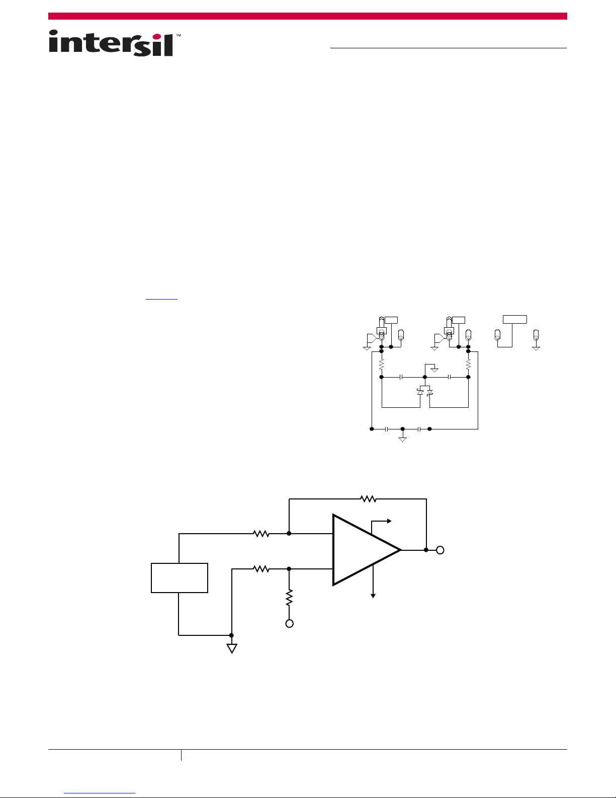
Power Supplies (Figure 1)
External power connections are made through the V+, V-, VREF,
and GND connections on the evaluation board. The circuit can
operate from a single supply or from dual supplies. For single
supply operation, the V- and GND pins are tied together to the
negative or ground reference of the power supply. For split
supplies, V+ and V- terminals connect to their respective
supply terminals. De-coupling capacitors C2 and C4 provide
low-frequency power-supply filtering, while additional
capacitors, C3 and C5, which are connected close to the part,
filter out high frequency noise. Anti-reverse diode D1 (optional)
protects the circuit in the momentary case of accidentally
reversing the power supplies to the evaluation board. The VREF
pin can be connected to ground to establish a ground
referenced input for split supply operation, or can be externally
set to any reference level for single supply operation.
J11
J12
V-
3
2
0.01µF
J8
1J61
2
0
R16
C2 C4
1
1µF 1µF
1
CLOSE TO DUT
C3
FIGURE 1. POWER SUPPLY CIRCUIT
D1
C5
0.01µF
V+
3
2
1
1
2
0
R31
3
2
1
J13
1
VREF
J14
1
PRECISION
SENSOR
July 26, 2011
AN1658.0
1
1-888-INTERSIL or 1-888-468-3774
R13/R23
100kΩ
INA-
R11/R24
10kΩ
R14/R21
10kΩ
V
REF
FIGURE 2. PRECISION AMPLIFIER WITH G = -10V/V
CAUTION: These devices are sensitive to electrostatic discharge; follow proper IC Handling Procedures.
INB-
INA+
INB+65
R18/R19
100kΩ
2
3
| Intersil (and design) is a trademark owned by Intersil Corporation or one of its subsidiaries.
8
-
ISL28208
TO +20V
V+
V-
+
GAIN = -10V/V
4
-4.5V TO -20V
All other trademarks mentioned are the property of their respective owners.
+4.5V
1/7
Copyright Intersil Americas Inc. 2011. All Rights Reserved.
V
OUT
Page 2
Application Note 1658
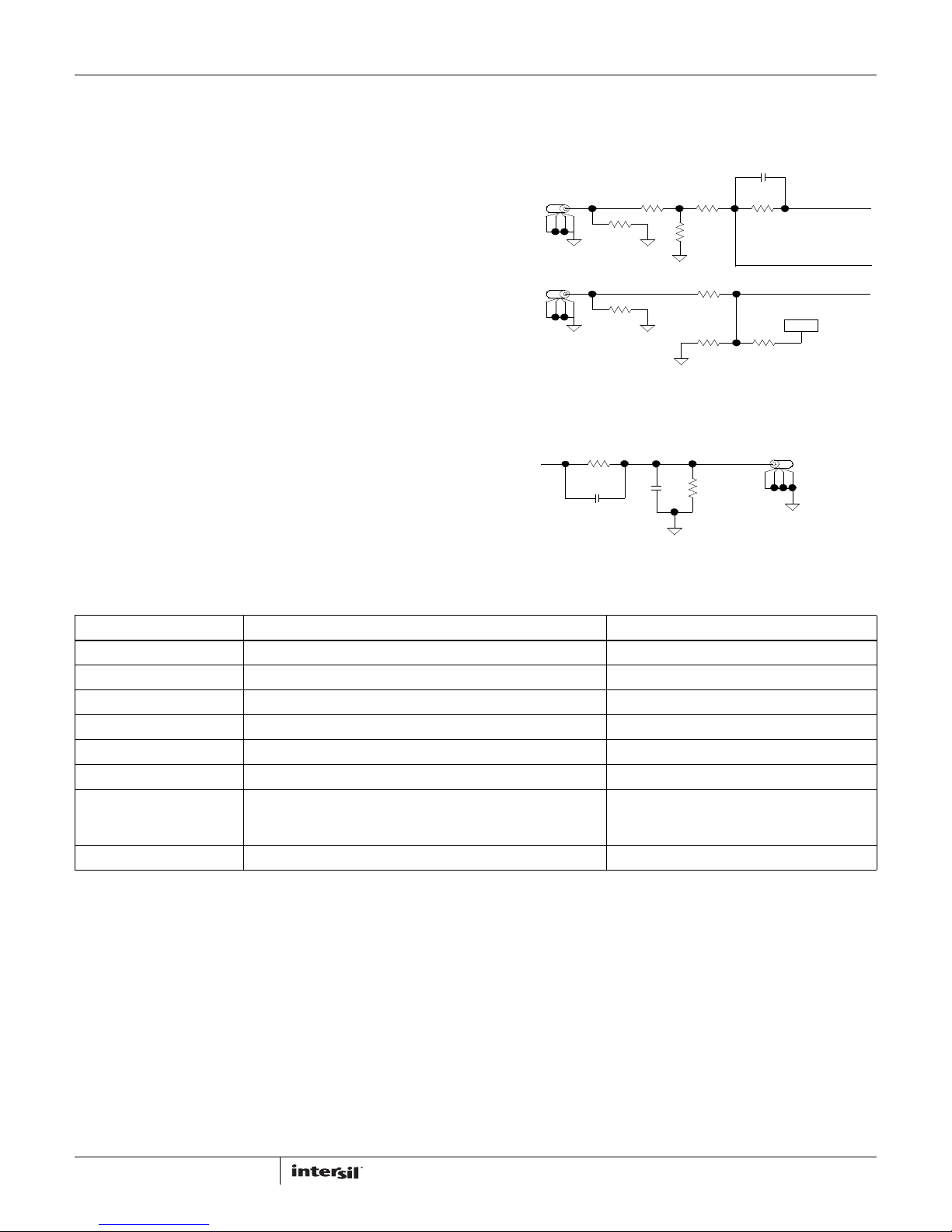
Amplifier Configuration (Figure 3)
The schematic of the op amp input stage with the components
supplied is shown in Figure 3, with a closed loop gain of 10V/V.
The differential amplifier gain is expressed in Equation 1:
V
( V
OUTVIN+
) RF(• RIN)⁄– V
IN-
+=
REF
(EQ. 1)
For single-ended input with an inverting gain G = -10V/V, the IN+
input is grounded and the signal is supplied to the IN- input. VREF
can be connected to a reference voltage between the V+ and Vsupply rails. For non-inverting operation with G = 11V/V, the INinput is grounded and the signal is supplied to the IN+ input. The
non-inverting gain is strongly dependent on any resistance from
IN- to GND. For good gain accuracy, a 0Ω resistor should be
installed on the empty R5 pad.
User-selectable Options
(Figures 3 and 4)
Component pads are included to enable a variety of
user-selectable circuits to be added to the amplifier inputs, the
VREF input, outputs and the amplifier feedback loops.
A voltage divider (Figure 3, R18 and R15) can be added to
establish a power supply-tracking common mode reference
using the VREF input. The inverting and non-inverting inputs have
additional resistor placements for adding input attenuation, or to
establish input DC offsets through the VREF pin.
The output (Figure 4) also has additional resistor and capacitor
placements for filtering and loading.
NOTE: Operational amplifiers are sensitive to output capacitance
and may oscillate. In the event of oscillation, reduce output
capacitance by using shorter cables, or add a resistor in series
with the output.
C1
OPEN
DNP
R13R11
100k
R18R15
100k
FROM V
VREF
J15
OUTA
TO INA -
TO INA +
OUT A
IN-A
IN+A
V
OUT_A
J1
J2
R26
0
C6
OPEN
R4
R1
0
DNP
R2
DNP
FIGURE 3. INPUT STAGE
C8
FIGURE 4. OUTPUT STAGE
R5
OPEN
10k
DNP
R14
10k
DNP
R28
TABLE 1. ISL28208SOICEVAL2Z COMPONENTS PARTS LIST
DEVICE # DESCRIPTION COMMENTS
C2, C4 CAP, SMD, 1206, 1µF, 50V, 10%, X7R, ROHS Power Supply Decoupling
C3, C5 CAP, SMD, 0603, 0.01µF, 50V, 10%, X7R, ROHS Power Supply Decoupling
C1, C6, C7, C8, C9, C10 CAP, SMD, 0603, DNP-PLACE HOLDER, ROHS User selectable capacitors - not populated
D1 40V DUAL SERIES SCHOTTKY BARRIER DIODE Reverse Power Protection
R11, R14, R21, R24 RESISTOR, SMD, 0603, 10kΩ, 1%, 1/16W, ROHS Gain Setting Resistor
R13, R23 RESISTOR, SMD, 0603, 100kΩ, 1%, 1/16W, ROHS Gain Setting Feedback Resistor
R1-R3, R5-R8, R10, R12, R15,
R17, R20, R22, R28-R30,
R32, R34-R36
U1 (ISL28208FBZ) ISL28208FBZ, IC PRECISION LOW NOSIE JFET OP AMP, SOIC, ROHS
RESISTOR, SMD, 0603, DNP-PLACE HOLDER, ROHS User selectable resistors - not populated
2
AN1658.0
July 26, 2011
Page 3

Application Note 1658
ISL28208SOICEVAL2Z Top View
Intersil Corporation reserves the right to make changes in circuit design, software and/or specifications at any time without notice. Accordingly, the reader is
cautioned to verify that the Application Note or Technical Brief is current before proceeding.
For information regarding Intersil Corporation and its products, see www.intersil.com
3
AN1658.0
July 26, 2011
Page 4

Application Note 1658
4
AN1658.0
July 26, 2011
ISL28208SOICEVAL2Z Schematic Diagram
OUT IN+ IN-IN+ NODE OUTIN- NODE
CLOSE TO DUT
2
2
1
R29
R26
OPEN
0.01µF0.01µF
1
R30
2
J21
1
21
R31
1
R16
2
1
J23
2
1
J18
21
J24
2
J22
21
2
1
J20
2
1
J19
2
1
J17
21
R36
1
R3221R34
2
1
R35
3
2
1
D1
2
1
C1
21
R22
21
R19
21
R21
21
R20
21
C10
21
R8
21
R7
2
1
R5
2
1
R4
2
1
R24
C2 C4
C3
C5
5
4
3
2
1
J15
5
4
3
2
1
J16
5
4
3
2
1
J2
5
4
3
2
1
J1
5
4
3
2
1
J3
5
4
3
2
1
J4
3
2
1
J11
1
J14
1
J12
1
J13
3
2
1J61
J8
21
21
R27
21
C7
21
C6
21
C8
21
C9
21
R1
2
21
R25
21
R23
2
1
R6
2
1
R17
21
R2
21
R28
21
R14
21
R3
21
R18
21
R15
2
1
R12
21
R10
2
1
R13
21
R11
8
7
6
54
3
2
1
U1
10k
100k
0
0
SOIC8
DNP
0
DNP
OPEN
DNP
OPEN
OPEN
0
DNP
DNP
DNP
DNP
OPEN
DNP
DNP
DNP
DNP
DNP
DNP
DNP
DNP
DNP
DNP
OPEN
DNP
DNP
10k 100k
100k
10k
10k
0
0 DNP
100k
1µF 1µF
VREF
VREF
V+V-
5
6
7
8
3
4
1
2
GENERIC
PACK.
OUT A
OUT B
IN-A
IN+A
IN-B
IN+B
 Loading...