

查询ISL28197FHZ-T7供应商
®
ISL28196, ISL28197
Data Sheet FN6152.3November 5, 2007
Ultra-Small, 800nA and 2.5µA Single
Supply, Rail-to-Rail Input/Output (RRIO)
Comparators
The ISL28196 and ISL28197 are micropower comparators
optimized for low-power applications. The parts are
designed for single-supply operation from 1.8V to 5.5V. The
ISL28197 typically consumes 800nA of supply current and
the ISL28196 typically consumes 2.5µA of supply current.
Both parts feature rail-to-rail input and output swing (RRIO),
allowing for maximum battery usage. The ISL28196 features
a propagation delay of 150µs and the ISL28197 features a
propagation delay of 0.6ms.
Equipped with an ENABLE pin (EN), both parts draw
typically 2nA when off. The combination of small footprint,
low power, single supply, and rail-to-rail operation makes
them ideally suited for all battery operated devices.
Pinouts
ISL28196, ISL28197
(6 LD SOT-23)
TOP VIEW
1
OUT
GND
2
+-
IN+
3
ISL28196, ISL28197
(6 LD 1.6X1.6X0.5 µTDFN)
TOP VIEW
1
IN-
-
2
GND
IN+
+
3
6
V+
EN
5
IN-
4
6
V+
5
EN
OUT
4
Features
• Typical Supply Current 800nA (ISL28197)
• Typical Supply Current 2.5µA (ISL28196)
• Ultra-Low Single-Supply Operation Down to +1.8V
• Rail-to-Rail Input/Output Voltage Range (RRIO)
• 150µs Typical Propagation Delay (ISL28196)
• 0.6ms Typical Propagation Delay (ISL28197)
• ENABLE Pin Feature
• Push-Pull Output
• -40°C to +125°C Operation
• Pb-Free (RoHS Compliant)
Applications
• 2-Cell Alkaline Battery-Powered/Portable Systems
• Window Comparators
• Threshold Detectors/Discriminators
Ordering Information
PART
NUMBER
(Note 3)
ISL28196FHZ-T7*
(Note 1)
Coming Soon
ISL28196FRUZ-T7*
(Note 2)
ISL28197FHZ-T7*
(Note 1)
Coming Soon
ISL28197FRUZ-T7*
(Note 2)
NOTES:
1. These Intersil Pb-free plastic packaged products employ special Pbfree material sets; molding compounds/die attach materials and
100% matte tin plate PLUS ANNEAL - e3 termination finish, which is
RoHS compliant and compatible with both SnPb and Pb-free
soldering operations. Intersil Pb-free products are MSL classified at
Pb-free peak reflow temperatures that meet or exceed the Pb-free
requirements of IPC/JEDEC J STD-020.
2. These Intersil Pb-free plastic packaged products employ special Pbfree material sets; molding compounds/die attach materials and
NiPdAu plate - e4 termination finish, which is RoHS compliant and
compatible with both SnPb and Pb-free soldering operations. Intersil
Pb-free products are MSL classified at Pb-free peak reflow
temperatures that meet or exceed the Pb-free requirements of
IPC/JEDEC J STD-020.
3. Please refer to TB347 for details on reel specifications.
PART
MARKING
GABM 6 Ld SOT-23
M5 6 Ld 1.6x1.6x0.5 µTDFN
GABN 6 Ld SOT-23
M6 6 Ld 1.6x1.6x0.5 µTDFN
PACKAGE
(Pb-Free)
Tape and Reel
Tape and Reel
Tape and Reel
Tape and Reel
PKG.
DWG. #
MDP0038
L6.1.6x1.6A
MDP0038
L6.1.6x1.6A
1
CAUTION: These devices are sensitive to electrostatic discharge; follow proper IC Handling Procedures.
1-888-INTERSIL or 1-888-468-3774
| Intersil (and design) is a registered trademark of Intersil Americas Inc.
All other trademarks mentioned are the property of their respective owners.
Copyright Intersil Americas Inc. 2007. All Rights Reserved
ISL28196, ISL28197
Absolute Maximum Ratings (T
Supply Voltage (V+, V-) . . . . . . . . . . . . . . . . . . . . . . . . . . . . . . 5.75V
Supply Turn On Voltage Slew Rate . . . . . . . . . . . . . . . . . . . . . 1V/µs
Differential Input Current . . . . . . . . . . . . . . . . . . . . . . . . . . . . . . 5mA
Differential Input Voltage . . . . . . . . . . . . . . . . V-
Input Voltage . . . . . . . . . . . . . . . . . . . . . . . . . V-
ESD Rating
Human Body Model . . . . . . . . . . . . . . . . . . . . . . . . . . . . . . . . .3kV
Machine Model. . . . . . . . . . . . . . . . . . . . . . . . . . . . . . . . . . . .300V
=+25°C) Thermal Information
A
Thermal Resistance (Typical, Note 4) θ
6 Ld SOT-23 Package . . . . . . . . . . . . . . . . . . . . . . . 230
6 Ld µTDFN Package . . . . . . . . . . . . . . . . . . . . . . . 117.52
- 0.5V to V+ + 0.5V
- 0.5V to V+ + 0.5V
Output Short-Circuit Duration . . . . . . . . . . . . . . . . . . . . . . .Indefinite
Ambient Operating Temperature Range . . . . . . . . .-40°C to +125°C
Storage Temperature Range . . . . . . . . . . . . . . . . . .-65°C to +150°C
Operating Junction Temperature . . . . . . . . . . . . . . . . . . . . .+125°C
Pb-free reflow profile . . . . . . . . . . . . . . . . . . . . . . . . . .see link below
(°C/W)
JA
http://www.intersil.com/pbfree/Pb-FreeReflow.asp
CAUTION: Do not operate at or near the maximum ratings listed for extended periods of time. Exposure to such conditions may adversely impact product reliability and
result in failures not covered by warranty.
NOTE:
is measured with the component mounted on a high effective thermal conductivity test board in free air. See Tech Brief TB379 for details.
4. θ
JA
IMPORT ANT NOTE: A ll p arameters having Min/Max specificati ons are gua ranteed. Typ values are for information purposes only. Unless otherwise noted, all tests are at
the specified temperature and are pulsed tests, Therefore T
Electrical Specifications V
= 5V, V- = 0V, VCM = 2.5V, TA = +25°C, unless otherwise specified. Boldface limits apply over -40°C to
+
+125°C.
PARAMETER DESCRIPTION CONDITIONS
V
OS
I
OS
I
B
Input Offset Voltage -2
Input Offset Current -60
Input Bias Current -80
= TC = T
J
A
MIN
(Note 5) TYP
-0.1 2
-2.5
10 60
-100
15 80
-150
MAX
(Note 5) UNIT
mV
2.5
pA
100
pA
150
CMIR Common Mode Input Range Established by CMRR test 0 5 V
CMRR Common-Mode Rejection Ratio V
= 0.5V to 3.5V 70
CM
= 0V to 5V 60 dB
V
CM
70
PSRR Power Supply Rejection Ratio V+ = 1.8V to 5.0V 70
100 dB
100 dB
70
V
OUT
I
S,ON
Maximum Output Voltage Swing
R
terminated to V+/2
L
Output low, R
Output high, R
Supply Current, Enabled ISL28196 2.5 4.0
= 10kΩ 35 70 mV
L
= 10kΩ 4.930 4.950 V
L
µA
4.5
ISL28197 0.8 1.6
µA
2.0
I
S,OFF
V
SUPPLY
C
IN
Supply Current, Disabled EN = 0.4V 2 20
nA
50
Supply Voltage Range 1.8 5.5 V
Input Capacitance 5pF
ENABLE INPUT
V
V
I
ENH
I
ENL
INH
INL
Enable Pin High Level (V+)x(0.8) V
Enable Pin Low Level 0.4 V
Enable Pin Input Current VEN = 5V 30 150
200
Enable Pin Input Current VEN = 0V 30 150
200
nA
nA
2
FN6152.3
November 5, 2007
ISL28196, ISL28197
Electrical Specifications V
PARAMETER DESCRIPTION CONDITIONS
= 5V, V- = 0V, VCM = 2.5V, TA = +25°C, unless otherwise specified. Boldface limits apply over -40°C to
+
+125°C. (Continued)
MIN
(Note 5) TYP
MAX
(Note 5) UNIT
TIMING
t
± ISL28196 Propagation Delay Low to High and High to Low CL = 10pF , 20mV Overdrive 150 300 μs
PD
t
± ISL28197 Propagation Delay Low to High and High to Low CL = 10pF, 1.5V Overdrive 0.625 1.3 ms
PD
tR/t
F
ISL28196 Rise/Fall Time CL = 10pF 9 18 μs
ISL28197 Rise/Fall Time C
= 10pF 35 70 μs
L
NOTE:
5. Parts are 100% tested at +25°C. Over-temperature limits established by characterization and are not production tested.
Typical Performance Curves V
164
RL = INF
162
160
158
156
154
152
150
SUPPLY CURRENT (nA)
148
146
1.5 2.0 2.5 3.0 3.5 4.0 4.5 5.0
SUPPLY VOLTAGE (V)
= 5V, V- = 0V, VCM = 2.5V, unless otherwise specified.
+
730
RL = INF
720
710
700
690
SUPPLY CURRENT (nA)
680
670
1.5 2.0 2.5 3.0 3.5 4.0 4.5 5.0
SUPPLY VOLTAGE (V)
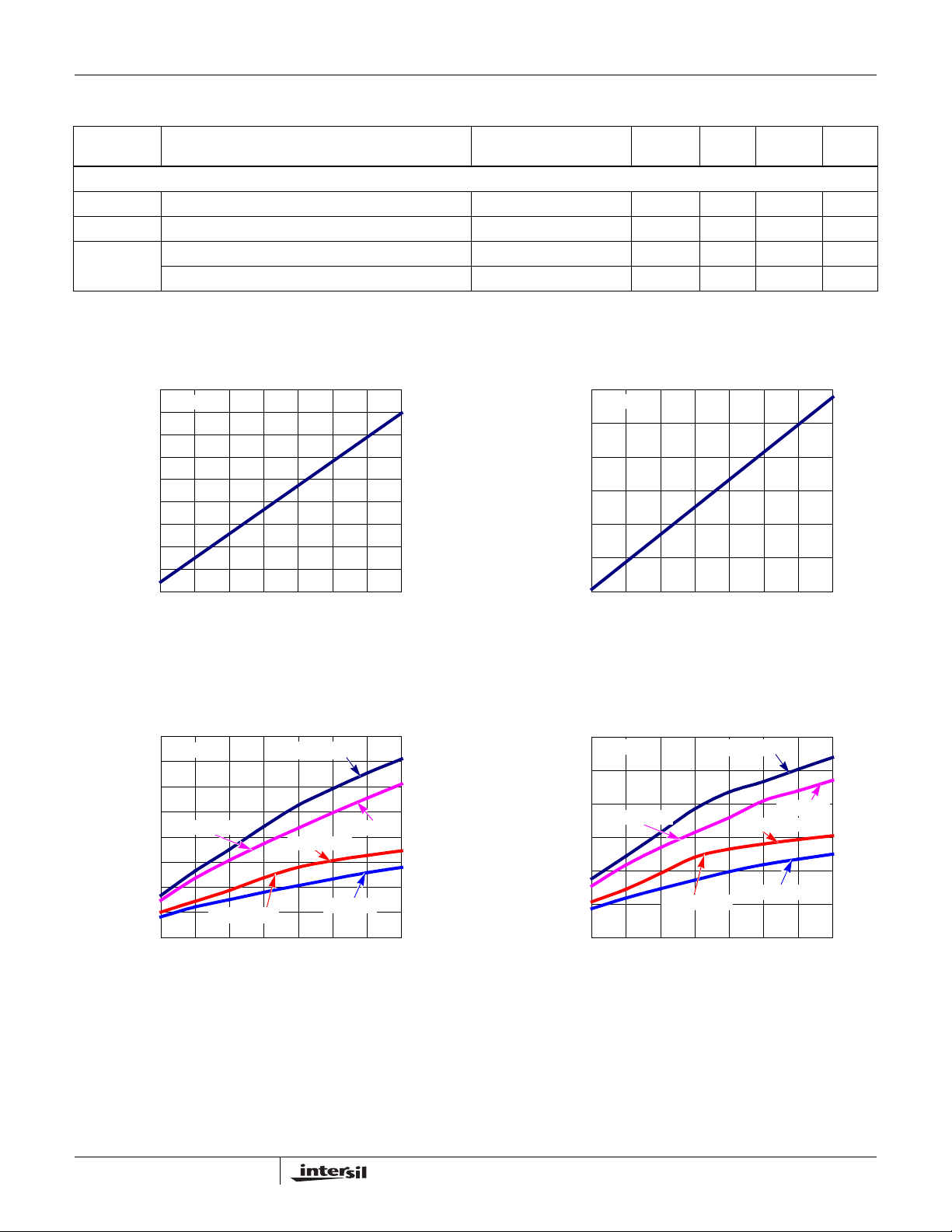
FIGURE 1. ISL28196 SUPPLY CURRENT vs SUPPLY VOLTAGE FIGURE 2. ISL28197 SUPPLY CURRENT vs SUPPLY VOLTAGE
400
RL = 10kΩ
350
300
250
200
150
DELAY (µs)
100
OD = 20mV
50
0
1.52.02.53.03.54.04.55.0
OD = 100mV
SUPPLY VOLTAGE (V)
RL TO GND
RL TO GND
RL TO V
RL TO V
+
+
FIGURE 3. ISL28196 PROP DELA Y vs SUPPLY VOL TAGE
(RISING EDGE)
1200
RL = 10kΩ
1000
800
OD = 20mV
600
DELA Y (µs)
400
200
0
1.5 2.0 2.5 3.0 3.5 4.0 4.5 5.0
OD = 100mV
SUPPLY VOLTAGE (V)
RL TO GND
RL TO GND
RL TO V
RL TO V
+
+
FIGURE 4. ISL28197 PROP DELA Y vs SUPPLY VOL TAGE
(RISING EDGE)
3
FN6152.3
November 5, 2007
ISL28196, ISL28197
Typical Performance Curves V
350
RL = 10kΩ
300
250
200
150
DELA Y (µs)
100
OD = 20mV
50
0
1.5 2.0 2.5 3.0 3.5 4.0 4.5 5.0
OD = 100mV
SUPPLY VOLTAGE (V)
= 5V, V- = 0V, VCM = 2.5V, unless otherwise specified. (Continued)
+
RL TO V
+
RL TO GND
RL TO V
+
RL TO GND
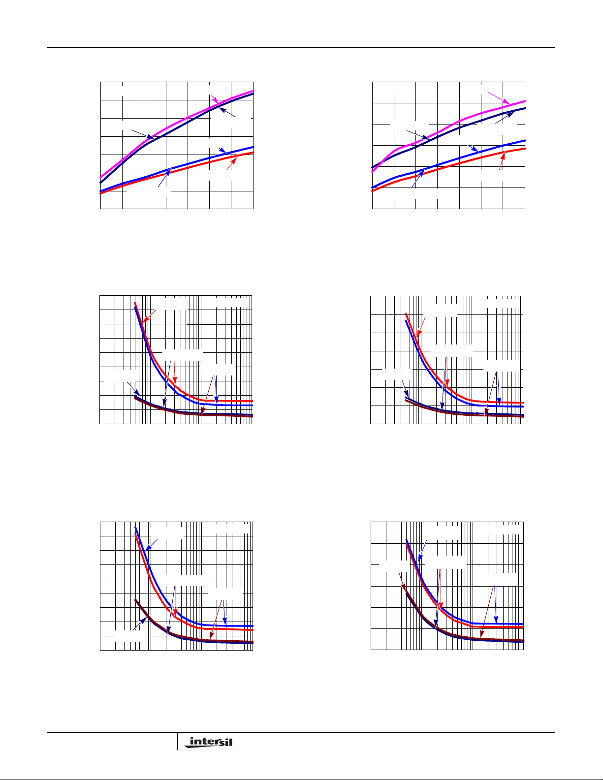
FIGURE 5. ISL28196 PROP DELA Y vs SUPPLY VOL TAGE
(FALLING EDGE)
900
800
700
600
500
400
V+ = 2V
DELAY (µs)
300
200
100
0
1 10 100 1000
V+ = 5V
RL TO GND
OVERDRIVE (mV)
RL = 10kΩ
RL TO V
+
FIGURE 7. ISL28196 PROP DELA Y vs OVERDRIVE
(RISING EDGE)
1200
RL = 10kΩ
1000
800
600
DELAY (µs)
400
200
OD = 20mV
OD = 100mV
0
1.5 2.0 2.5 3.0 3.5 4.0 4.5 5.0
SUPPLY VOLTAGE (V)
RL TO V
RL TO V
+
RL TO GND
+
RL TO GND
FIGURE 6. ISL28197 PROP DELA Y vs SUPPLY VOL TAGE
(FALLING EDGE)
3500
3000
2500
2000
1500
DELAY (µs)
V+ = 2V
1000
500
0
1 10 100 1000
V+ = 5V
RL TO GND
OVERDRIVE (mV)
RL = 10kΩ
RL TO V
+
FIGURE 8. ISL28197 PROP DELA Y vs OVERDRIVE
(RISING EDGE)
900
800
700
600
500
400
DELA Y ( μs)
300
200
100
V+ = 2V
0
1 10 100 1000
V+ = 5V
RL TO GND
OVERDRIVE (mV)
RL = 10kΩ
RL TO V
+
FIGURE 9. ISL28196 PROP DELA Y vs OVERDRIVE
(FALLING EDGE)
4
3000
2500
2000
V+ = 2V
1500
DELAY (μs)
1000
500
0
1 10 100 1000
V+ = 5V
RL TO GND
OVERDRIVE (mV)
RL = 10kΩ
RL TO V
+
FIGURE 10. ISL28197 PROP DELAY vs OVERDRIVE
(FALLING EDGE)
November 5, 2007
FN6152.3
ISL28196, ISL28197
Typical Performance Curves V
25
RL = 10Ω
20
15
10
OUTPUT CURRENT (mA)
5
0
1.0 1.5 2.0 2.5 3.0 3.5 4.0 4.5 5.0 5.5
SUPPLY VOLTAGE (V)
SINKING
= 5V, V- = 0V, VCM = 2.5V, unless otherwise specified. (Continued)
+
SOURCING
FIGURE 11. ISL28196 SHORT CIRCUIT CURRENT vs SUPPLY
VOLTAGE
3.0
2.8
2.6
2.4
2.2
2.0
1.8
1.6
ENABLE THRESHOLD (V)
1.4
1.2
1.0
1.5 2.02.53.03.54.04.55.0
SUPPLY VOLTAGE (V)
FIGURE 13. ISL28196 ENABLE THRESHOLD VOLT AGE vs
SUPPLY VOLTAGE
25
RL = 10Ω
20
15
10
OUTPUT CURRENT (mA)
5
0
1.0 1.5 2.0 2.5 3.0 3.5 4.0 4.5 5.0 5.5
SUPPLY VOLTAGE (V)
SINKING
SOURCING
FIGURE 12. ISL28197 SHORT CIRCUIT CURRENT vs SUPPLY
VOLTAGE
3.0
2.8
2.6
2.4
2.2
2.0
1.8
1.6
1.4
ENABLE THRESHOLD (V)
1.2
1.0
1.5 2.0 2.5 3.0 3.5 4.0 4.5 5.0
SUPPLY VOLTAGE (V)
SUPPLY VOLTAGE (V)
FIGURE 14. ISL28197 ENABLE THRESHOLD VOLT AGE vs
SUPPLY VOLTAGE
100
90
80
70
60
50
40
30
20
10
ENABLE TO OUTPUT DELAY (ms)
0
1.5 2.0 2.5 3.0 3.5 4.0 4.5 5.0
SUPPLY VOLTAGE (V)
FIGURE 15. ISL28196 ENABLE TO OUTPUT DELAY TIME vs
SUPPLY VOLTAGE
5
80
70
60
50
40
30
20
10
ENABLE TO OUTPUT DELAY (ms)
0
1.5 2.0 2.5 3.0 3.5 4.0 4.5 5.0
SUPPLY VOLTAGE (V)
FIGURE 16. ISL28197 ENABLE TO OUTPUT DELA Y TIME vs
SUPPLY VOLTAGE
FN6152.3
November 5, 2007

ISL28196, ISL28197
Typical Performance Curves V
1000
950
900
850
800
750
700
650
DISABLE TO OUTPUT DELAY (ns)
600
1.5 2.0 2.5 3.0 3.5 4.0 4.5 5.0
SUPPLY VOLTAGE (V)
= 5V, V- = 0V, VCM = 2.5V, unless otherwise specified. (Continued)
+
FIGURE 17. ISL28196 ENABLE LOW TO OUTPUT TURN-OFF
TIME vs SUPPLY VOLTAGE
4.5
N = 1000
4.0
3.5
3.0
2.5
2.0
1.5
SUPPLY CURRENT (µA)
1.0
0.5
-40 -20 0 20 40 60 80 100 120
TEMPERATURE (°C)
MAX
MEDIAN
MIN
FIGURE 19. ISL28196 SUPPLY CURRENT vs TEMPERATURE,
V
, V- = ±2.5V
+
1500
1400
1300
1200
1100
1000
900
800
700
DISABLE TO OUTPUT DELAY (ns)
600
1.5 2.0 2.5 3.0 3.5 4.0 4.5 5.0
SUPPLY VOLTAGE (V)
FIGURE 18. ISL28197 ENABLE LOW TO OUTPUT TURN-OFF
TIME vs SUPPLY VOLTAGE
1.8
N = 1000
1.6
1.4
1.2
1.0
0.8
0.6
0.4
SUPPLY CURRENT (µA)
0.2
0
-40 -20 0 20 40 60 80 100 120
MAX
MEDIAN
MIN
TEMPERATURE (°C)
FIGURE 20. ISL28197 SUPPLY CURRENT vs TEMPERATURE,
V+, V- = ±2.5V
90
N = 1000
80
70
60
50
(pA)
40
BIAS+
I
30
20
10
0
-40 -20 0 20 40 60 80 100 120
FIGURE 21. ISL28196 I
100
80
MAX
MEDIAN
MIN
TEMPERATURE (°C)
vs TEMPERATURE, V+, V- = ±2.5V FIGURE 22. ISL28197 I
BIAS+
60
(pA)
40
BIAS+
I
20
0
-20
-40 -20 0 20 40 60 80 100 120
6
N = 1000
MAX
MIN
TEMPERATURE (°C)
vs TEMPERATURE, V+, V- = ±2.5V
BIAS+
MEDIAN
FN6152.3
November 5, 2007

ISL28196, ISL28197
Typical Performance Curves V
120
N = 1000
100
80
(pA)
60
BIAS-
I
40
20
0
-40-200 20406080100120
FIGURE 23. ISL28196 I
V
70
N = 1000
60
50
40
(pA)
30
OS
I
20
10
0
-40-200 20406080100120
FIGURE 25. ISL28196 I
MAX
, V- = ±2.5V
+
MEDIAN
MIN
TEMPERATURE (°C)
vs TEMPERATURE,
BIAS-
MAX
MEDIAN
MIN
TEMPERATURE (°C)
vs TEMPERATURE, V+, V- = ±2.5V FIGURE 26. ISL28197 IOS vs TEMPERATURE, V+, V- = ±2.5V
OS
= 5V, V- = 0V, VCM = 2.5V, unless otherwise specified. (Continued)
+
120
N = 1000
100
80
(pA)
60
BIAS-
I
40
20
0
-40 -20 0 20 40 60 80 100 120
TEMPERATURE (°C)
FIGURE 24. ISL28197 I
V
, V- = ±2.5V
+
50
N = 1000
45
40
35
30
(pA)
25
OS
I
20
15
10
5
0
-40-200 20406080100120
vs TEMPERATURE,
BIAS-
TEMPERATURE (°C)
MAX
MEDIAN
MIN
MAX
MEDIAN
MIN
3
N = 1000
2
1
(µV)
0
OS
V
-1
-2
-3
-40 -20 0 20 40 60 80 100 120
FIGURE 27. ISL28196 V
V
= 2.5V
IN
MAX
MEDIAN
MIN
TEMPERATURE (°C)
vs TEMPERATURE, V+, V- = ±2.5V
OS
7
3
N = 1000
2
1
(µV)
0
OS
V
-1
-2
-3
-40 -20 0 20 40 60 80 100 120
FIGURE 28. ISL28197 V
V
= 2.5V
IN
MAX
MEDIAN
MIN
TEMPERATURE (°C)
vs TEMPERATURE, V+, V- = ±2.5V
OS
FN6152.3
November 5, 2007

ISL28196, ISL28197
Typical Performance Curves V
105
N = 1000
100
95
90
85
CMRR (dB)
80
75
70
-40 -20 0 20 40 60 80 100 120
TEMPERATURE (°C)
FIGURE 29. ISL28196 CMRR vs TEMPERATURE,
VCM = 0.5V TO 3.5, V
110
N = 1000
105
100
95
90
85
PSRR (dB)
80
75
70
-40 -20 0 20 40 60 80 100 120
MAX
TEMPERATURE (°C)
MAX
MEDIAN
MIN
MIN
, V- = ±2.5V
+
MEDIAN
= 5V, V- = 0V, VCM = 2.5V, unless otherwise specified. (Continued)
+
105
N = 1000
100
95
90
85
CMRR (dB)
80
75
70
-40 -20 0 20 40 60 80 100 120
MAX
MEDIAN
MIN
TEMPERATURE (°C)
FIGURE 30. ISL28197 CMRR vs TEMPERATURE,
VCM = 0.5V TO 3.5, V+, V- = ±2.5V
110
N = 1000
105
100
95
90
85
PSRR (dB)
80
75
70
-40 -20 0 20 40 60 80 100 120
MAX
MEDIAN
TEMPERATURE (°C)
MIN
FIGURE 31. ISL28196 PSRR vs TEMPERATURE,
V
, V- = ±0.9V TO ±2.5V
+
4.956
N = 1000
4.954
4.952
4.950
4.948
(V)
4.946
OUT
V
4.944
4.942
4.940
4.938
4.936
-40 -20 0 20 40 60 80 100 120
FIGURE 33. ISL28196 V
V
+
MAX
MIN
TEMPERATURE (°C)
HIGH vs TEMPERATURE,
, V- = ±2.5V, RL = 10k
OUT
MEDIAN
FIGURE 32. ISL28197 PSRR vs TEMPERATURE,
V+, V- = ±0.9V TO ±2.5V
4.955
N = 1000
4.954
4.953
4.952
4.951
(V)
4.950
OUT
V
4.949
4.948
4.947
4.946
4.945
-40-200 20406080100120
FIGURE 34. ISL28197 V
V
, V- = ±2.5V, RL = 10k
+
MEDIAN
TEMPERATURE (°C)
HIGH vs TEMPERATURE,
OUT
MAX
MIN
8
FN6152.3
November 5, 2007

ISL28196, ISL28197
Typical Performance Curves V
50
N = 1000
45
40
35
(mV)
30
OUT
V
25
20
15
-40-200 20406080100120
FIGURE 35. ISL28196 V
V
, V- = ±2.5V, RL = 10k
+
270
N = 1000
250
230
210
190
+ PROP DELAY (µs)
170
150
-40 -20 0 20 40 60 80 100 120
MAX
MEDIAN
MIN
TEMPERATURE (°C)
LOW vs TEMPERA TURE,
OUT
MAX
MEDIAN
TEMPERATURE (°C)
+
MIN
FIGURE 37. ISL28196 POSITIVE PROP DELAY vs
TEMPERATURE 50% TO 20%, V
= 5V, V- = 0V, VCM = 2.5V, unless otherwise specified. (Continued)
39
N = 1000
37
35
33
(mV)
31
OUT
V
29
27
25
-40-200 20406080100120
FIGURE 36. ISL28197 V
V
, V- = ±2.5V, RL = 10k
+
1750
1550
1350
1150
+ PROP DELAY (µs)
N = 1000
950
750
550
350
150
-40 -20 0 20 40 60 80 100 120
MAX
MEDIAN
MIN
TEMPERATURE (°C)
LOW vs TEMPERATURE,
OUT
MAX
MEDIAN
MIN
TEMPERATURE (°C)
FIGURE 38. ISL28197 POSITIVE PROP DELA Y vs
= 5V
+
TEMPERATURE 50% TO 20%, V+ = 5V
220
200
180
160
140
- PROP DELAY (µs)
120
100
N = 1000
MAX
MEDIAN
MIN
-40 -20 0 20 40 60 80 100 120
TEMPERATURE (°C)
FIGURE 39. ISL28196 NEGATIVE PROP DELAY vs
TEMPERATURE 50% TO 20%, V
= 5V
+
9
1700
1500
1300
1100
- PROP DELAY (µs)
N = 1000
MAX
900
700
500
300
100
-40 -20 0 20 40 60 80 100 120
MEDIAN
MIN
TEMPERATURE (°C)
FIGURE 40. ISL28197 NEGATIVE PROP DELAY vs
TEMPERATURE 50% TO 20%, V+ = 5V
FN6152.3
November 5, 2007

ISL28196, ISL28197
Typical Performance Curves V
8.0
N = 1000
7.5
7.0
6.5
6.0
5.5
+ PROP DELAY (µs)
5.0
4.5
-40-200 20406080100120
FIGURE 41. ISL28196 FALL TIME vs TEMPERA TURE 20% TO
80%, V
MAX
MEDIAN
TEMPERATURE (°C)
= 5V
+
MIN
= 5V, V- = 0V, VCM = 2.5V, unless otherwise specified. (Continued)
+
54.5
49.5
44.5
39.5
34.5
29.5
24.5
19.5
+ PROP DELAY (µs)
14.5
9.5
4.5
-40 -20 0 20 40 60 80 100 120
MEDIAN
TEMPERATURE (°C)
FIGURE 42. ISL28197 FALL TIME vs TEMPERATURE 20% T O
80%, V+ = 5V
MAX
MIN
Pin Descriptions
ISL28196,
ISL28197
(6 LD SOT-23)
1 4 OUT Circuit 3 Comparator output
2 2 GND Circuit 4 GROUND terminal
3 3 IN+ Circuit 1 Comparator non-inverting input
4 1 IN- Circuit 1 Comparator inverting input
5 5 EN Circuit 2 Comparator enable pin; Logic “1” selects the enabled state: Logic “0” selects the
6 6 V+ Circuit 4 Positive power supply
ISL28196,
ISL28197
(6 LD µTDFN) PIN NAME
EQUIVALENT
CIRCUIT DESCRIPTION
disabled state
N = 1000
V+
LOGIC
IN-
IN+
V-
CIRCUIT 1
PIN
CIRCUIT 2
Applications Information
Introduction
The ISL28196 and ISL28197 are CMOS rail-to-rail input and
output (RRIO) micropower comparators. These devices are
designed to operate from single supply (1.8V to 5.5V) and
have an input common mode range that extends to the
positive rail and to the negative supply rail for true rail-to-rail
performance. The CMOS output can swing within tens of
millivolts to the rails. Featuring worst case maximum supply
currents of only 4.5µA and 2µA for the ISL28196 and
ISL28197 respectively, these comparators are ideally suited
for solar and battery powered applications.
V+
V-
V+
V-
CIRCUIT 4
CAPACITIVELY
COUPLED
ESD CLAMP
100Ω
CIRCUIT 3
V+
OUT
V-
Input Protection
All input terminals have internal ESD protection diodes to both
positive and negative supply rails, limiting the input voltage to
within one diode beyond the suppl y rails . Both the ISL28196
and ISL28197 have a maximum input differential voltage that
extends beyond the rails (
V + 0.5V to -V - 0.5V).
+
Rail-to-Rail Output
A pair of complementary MOSFET devices are used to
achieve the rail-to-rail output swing. The NMOS sinks
current to swing the output in the negative direction. The
PMOS sources current to swing the output in the positive
direction. The ISL28196 and ISL28197 with a 100kΩ load
will swing to within 6mV of the positive supply rail and within
3mV of ground.
10
FN6152.3
November 5, 2007

ISL28196, ISL28197
Break-Before-Make Operation of the Output
The output circuit has a break-before-make response. This
means that the P-Channel turns off before the N-Channel
turns on during a high to low transition of the output
(reference Figure 43). Likewise, the N-Channel turns off
before the P-Channel turns on during a low to high transition.
This results in different propagation delay times depending
upon where the output load resistor is tied to. If the load
resistor is tied to ground, (Figure 44A) then the propagation
delay is controlled by the P-Channel. For a high to low
transition the propagation delay does not include the
additional break-before-make time because the load resistor
will pull the output low once the P-Channel has turned off.
BREAK-BEFORE-MAKE
P-CH OFF
P-CH ON
N-CH OFF
N-CH ON
FIGURE 43. MAKE-BEFORE-BREAK ACTION OF THE
OUTPUT STAGE
During the low to high transition, however, if the load resistor
is tied to ground, then the additional break-before-make time
is added to the propagation delay time because the output
won’t pull high until the P-Channel turns on.
V
+
+
-
FIGURE 44A. RL TO GND
V
+
+
-
FIGURE 44B. R
FIGURE 44. CONNECTION OF R
ISL28196 AND ISL28197
OUTPUT STAGE
v
+
P-CH ON
N-CH OFF
R
L
R
L
P-CHANNEL
N-CHANNEL
VOUT
VOUT
TO V+
L
TO GND AND V+
L
VOUT
If the load resistor is tied to V+ (Figure 44B) then the
propagation delay is controlled by the N-Channel. For this
condition, the additional delay time is added to the high to
low transition because the output won’t pull low until the
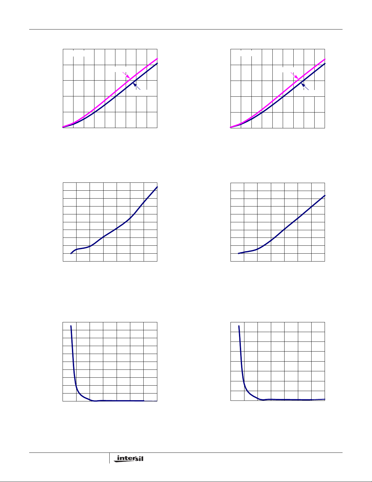
N-Channel turns on. Figures 3 through 10 show the
differences in propagation delay depending upon where the
load is tied.
Propagation Delay
The input to output propagation delay has a dependency on
power supply voltage, overdrive and whether the output is
sourcing or sinking current. Figures 3 and 5 show a
decreasing time propagation delay vs supply voltage for the
ISL28196 and Figure 4 shows a similar behavior for the
ISL28197. The output break-before-make mechanism
results in a difference in propagation delay, depending on
whether the output stage NMOS and PMOS are sourcing or
sinking current. This delay difference is shown in the figures
as a function of where the load is terminated (+V or -V) and
also as a function of supply voltage. The dependence of
propagation delay as a function of power supply voltage and
input overdrive (from 5mV to 1V) is shown in Figures 7 and 9
for the ISL28196, and Figures 8 and 10 for the ISL28197.
Enable Feature
Both parts offer an EN pin, which enables the device when
pulled high. The enable threshold is referenced to the -V
terminal and has a level proportional to the total supply
voltage (reference Figures 13 and 14 for EN Threshold vs
Supply Voltage). The enable circuit has a delay time that
changes as a function of supply voltage. Figures 23 through
26 show the effect of supply voltage on the enable and
disable times. For supply voltages less than 3V, it is
recommended that the user account for the increase
enable/disable delay time.
In the disabled state (output in a high impedance state), the
supply current is reduced to a typical of only 2nA. By
disabling the devices, multiple parts can be connected
together as a MUX. In this configuration, the outputs are tied
together in parallel and a channel can be selected by the EN
pin. The EN pin should never be left floating. The EN pin
should be connnected directly to the V+ supply when not in
use.
Proper Layout Maximizes Performance
To achieve the maximum performance of the high input
impedance, care should be taken in the circuit board layout.
The PC board surface must remain clean and free of
moisture to avoid leakage currents between adjacent traces.
Surface coating of the circuit board will reduce surface
moisture and provide a humidity barrier, reducing parasitic
resistance on the board. When input leakage current is a
concern, the use of guard rings around the comparator
inputs will further reduce leakage currents.
11
FN6152.3
November 5, 2007

ISL28196, ISL28197
Power Dissipation
It is possible to exceed the +150°C maximum junction
temperatures under certain load and power-supply
conditions. It is therefore important to calculate the
maximum junction temperature (T
to determine if power supply voltages, load conditions, or
package type need to be modified to remain in the safe
operating area. These parameters are related in Equation 1:
T
JMAXTMAXθJA
xPD
()+=
MAXTOTAL
where:
) for all applications
JMAX
(EQ. 1)
•P
DMAXTOTAL
is the sum of the maximum power
dissipation of each amplifier in the package (PD
•PD
for each amplifier can be calculated as shown in
MAX
Equation 2:
PD
MAX
2*VSI
( - V
SMAXVS
OUTMAX
)
×+×=
where:
•T
• θ
•PD
•V
•I
•V
= Maximum ambient temperature
MAX
= Thermal resistance of the package
JA
= Maximum power dissipation of 1 amplifier
MAX
= Supply voltage (Magnitude of V+ and V-)
S
= Maximum supply current of 1 amplifier
MAX
OUTMAX
= Maximum output voltage swing of the
application
= Load resistance
•R
L
MAX
V
OUTMAX
----------------------------
R
L
)
(EQ. 2)
12
FN6152.3
November 5, 2007

ISL28196, ISL28197
Ultra Thin Dual Flat No-Lead Plastic Package (UTDFN)
PIN 1
REFERENCE
2X
0.15 C
2X
6X
E
64
13
0.15 C
TOP VIEW
46
D2
31
BOTTOM VIEW
0.10 C
0.08 C
SIDE VIEW
1.00 REF
CO.2
E2
A
B
D
e
L
DAP SIZE 1.30 x 0.76
b6X
0.10 CAB
DETAIL A
C
A3
SEATING
PLANE
A
L6.1.6x1.6A
6 LEAD ULTRA THIN DUAL FLAT NO-LEAD PLASTIC PACKAGE
MILLIMETERS
SYMBOL
NOTESMIN NOMINAL MAX
A 0.45 0.50 0.55 A1 - - 0.05 A3 0.127 REF -
A1
b 0.15 0.20 0.25 -
D 1.55 1.60 1.65 4
D2 0.40 0.45 0.50 -
E 1.55 1.60 1.65 4
E2 0.95 1.00 1.05 -
e 0.50 BSC -
L 0.25 0.30 0.35 -
M
NOTES:
Rev. 1 6/06
1. Dimensions are in mm. Angles in degrees.
2. Coplanarity applies to the exposed pad as well as the terminals.
Coplanarity shall not exceed 0.08mm.
3. Warpage shall not exceed 0.10mm.
4. Package length/package width are considered as special
characteristics.
5. JEDEC Reference MO-229.
6. For additional information, to assist with the PCB Land Pattern
Design effort, see Intersil Technical Brief TB389.
0.127±0.008
A1
0.50
1.00
1.25
DETAIL A
0.25
0.45
0.30
LAND PATTERN
0.127 +0.058
-0.008
TERMINAL THICKNESS
1.00
2.00
6
13
FN6152.3
November 5, 2007

SOT-23 Package Family
ISL28196, ISL28197
2 3
0.15 DC
2X
C
SEATING
PLANE
E1
5
0.15 A-BC
2X
0.10 C
NX
(L1)
e1
A
6
N
4
D
MDP0038
SOT-23 PACKAGE FAMILY
SYMBOL
MILLIMETERS
TOLERANCESOT23-5 SOT23-6
A 1.45 1.45 MAX
A1 0.10 0.10 ±0.05
E
A2 1.14 1.14 ±0.15
b 0.40 0.40 ±0.05
321
e
0.20
B
b
NX
M
0.20 C
2X
DC A-B
c 0.14 0.14 ±0.06
D 2.90 2.90 Basic
E 2.80 2.80 Basic
E1 1.60 1.60 Basic
e 0.95 0.95 Basic
e1 1.90 1.90 Basic
L 0.45 0.45 ±0.10
L1 0.60 0.60 Reference
1 3
D
N 5 6 Reference
Rev. F 2/07
NOTES:
A2
1. Plastic or metal protrusions of 0.25mm maximum per side are not
included.
2. Plastic interlead protrusions of 0.25mm maximum per side are not
A1
included.
3. This dimension is measured at Datum Plane “H”.
4. Dimensioning and tolerancing per ASME Y14.5M-1994.
5. Index area - Pin #1 I.D. will be located within the indicated zone
(SOT23-6 only).
H
6. SOT23-5 version has no center lead (shown as a dashed line).
A
c
L
0°
GAUGE
PLANE
+3°
-0°
0.25
All Intersil U.S. products are manufactured, assembled and tested utilizing ISO9000 quality systems.
Intersil Corporation’s quality certifications can be viewed at www.intersil.com/design/quality
Intersil products are sold by description only. Intersil Corporation reserves the right to make changes in circuit design, software and/or specifications at any time without
notice. Accordingly, the reader is cautioned to verify that data sheets are current before placing orders. Information furnished by Intersil is believed to be accurate and
reliable. However, no responsibility is assumed by Intersil or its subsidiaries for its use; nor for any infringements of patents or other rights of third parties which may result
from its use. No license is granted by implicat ion or oth erwise u nde r any p a tent or p at ent r ights of Intersil or its subsidiaries.
For information regarding Intersil Corporation and its products, see www.intersil.com
14
FN6152.3
November 5, 2007
 Loading...