

®
ISL28190, ISL28290
Data Sheet April 13, 2007
Single and Dual Ultra-Low Noise,
Ultra-Low Distortion, Rail-to-Rail, Op Amp
The ISL28190 and ISL28290 are tiny single and dual
ultra-low noise, ultra-low distortion operational amplifiers.
Fully specified to operated down to +3V single supply. These
amplifiers have outputs that swing rail-to-rail, and an input
common mode voltage that extends below ground (ground
sensing).
The ISL28190 and ISL28290 are unity gain stable with an
input referred voltage noise of 1nV/√Hz. Both parts feature
nd
2
and 3rd harmonic distortion of -87dBc and -90dBc,
respectively.
The ISL28190 is available in the space-saving 6 Ld µTDFN
(1.6mm x 1.6mm) and SOT-23 packages. The ISL28290 is
available in the 10 Ld µTQFN (1.8mm x 1.4mm) and MSOP
packages. All devices are guaranteed over -40°C to +125°C.
Ordering Information
PART NUMBER
(Note)
ISL28190FHZ-T7 GABH 3k pcs 6 Ld SOT-23 MDP0038
Coming Soon
ISL28190FRUZ-TK
ISL28290FUZ 8290Z 50/tube 10 Ld MSOP MDP0043
ISL28290FUZ-T7 8290Z 1.5k pcs 10 Ld MSOP MDP0043
Coming Soon
ISL28290FRUZ-T7
NOTE: Intersil Pb-free plus anneal products employ special Pb-free
material sets; molding compounds/die attach materials and 100% matte
tin plate termination finish, which are RoHS compliant and compatible
with both SnPb and Pb-free soldering operations. Intersil Pb-free
products are MSL classified at Pb-free peak reflow temperatures that
meet or exceed the Pb-free requirements of IPC/JEDEC J STD-020.
PART
MARKING
TAPE &
REEL
1k pcs 6 Ld μTDFN L6.1.6x1.6A
1k pcs 10 Ld μTQFN L10.1.8x1.4A
PACKAGE
(Pb-free)
PKG.
DWG. #
FN6247.3
Features
•1nV/√Hz input voltage noise
• Harmonic Distortion -87dBc, -90dBc, f
= 1MHz
o
• 170MHz -3dB bandwidth
• 50V/µs slew rate
• 700µV maximum offset voltage
• 10µA typical input bias current
• 103dB typical CMRR
• 3V to 5.5V single supply voltage range
• Rail-to-rail output
• Ground sensing
• Enable pin
• Pb-free plus anneal available (RoHS compliant)
Applications
• Low noise signal processing
• Low noise microphones/preamplifiers
• ADC buffers
• DAC output amplifiers
• Digital scales
• Strain gauges/sensor amplifiers
• Radio systems
• Portable equipment
• Infrared detectors
1
CAUTION: These devices are sensitive to electrostatic discharge; follow proper IC Handling Procedures.
1-888-INTERSIL or 1-888-468-3774
| Intersil (and design) is a registered trademark of Intersil Americas Inc.
Copyright © Intersil Americas Inc. 2006, 2007. All Rights Reserved.
All other trademarks mentioned are the property of their respective owners.
Pinouts
ISL28190
(6 LD SOT-23)
TOP VIEW
ISL28190, ISL28290
ISL28190
(6 LD 1.6X1.6X0.5 µTDFN)
TOP VIEW
OUT
IN+
1
V-
2
3
6
V +
5
-+
ENABLE
IN-
4
ISL28290
(10 LD MSOP)
TOP VIEW
1
OUT_A
2
IN-_A
IN+_A
ENABLE_A ENABLE_B
+
3
4
V-
5 6
10
V+
OUT_B
9
IN-_B
8
+
7
IN+_B
7
IN-_A
IN+_A
1
OUT
2
IN-
IN+
3
ISL28290
(10 Ld μTQFN)
TOP VIEW
OUT_A
10
1
-
+
2
V+
-+
V+
9
-
+
543
ENABLE_A
ENABLE_B
6
V+
5
ENABLE
4
V-
OUT_B
8
7
6
IN-_B
IN+_B
2
FN6247.3
April 13, 2007
ISL28190, ISL28290
Absolute Maximum Ratings (T
Supply Voltage. . . . . . . . . . . . . . . . . . . . . . . . . . . . . . . . . . . . . . 5.5V
Supply Turn On Voltage Slew Rate . . . . . . . . . . . . . . . . . . . . . 1V/μs
Differential Input Current . . . . . . . . . . . . . . . . . . . . . . . . . . . . . . 5mA
Differential Input Voltage . . . . . . . . . . . . . . . . . . . . . . . . . . . . . . 0.5V
Input Voltage . . . . . . . . . . . . . . . . . . . . . . . . . V-
ESD Tolerance
Human Body Model . . . . . . . . . . . . . . . . . . . . . . . . . . . . . . . . .3kV
Machine Model. . . . . . . . . . . . . . . . . . . . . . . . . . . . . . . . . . . .300V
= +25°C) Thermal Information
A
Thermal Resistance θ
6 Ld SOT-23 Package . . . . . . . . . . . . . . . . . . . . . . . 230
6 Ld µTDFN Package . . . . . . . . . . . . . . . . . . . . . . . 120
- 0.5V to V+ + 0.5V
10 Ld MSOP Package . . . . . . . . . . . . . . . . . . . . . . . 115
6 Ld µTQFN Package . . . . . . . . . . . . . . . . . . . . . . . 143
Ambient Operating Temperature Range . . . . . . . . .-40°C to +125°C
Storage Temperature Range . . . . . . . . . . . . . . . . . .-65°C to +150°C
Operating Junction Temperature . . . . . . . . . . . . . . . . . . . . . +125°C
(°C/W)
JA
Pb-free reflow profile . . . . . . . . . . . . . . . . . . . . . . . . . .see link below
http://www.intersil.com/pbfree/Pb-FreeReflow.asp
CAUTION: Stresses above those listed in “Absolute Maximum Ratings” may cause permanent damage to the device. This is a stress only rating and operation of the
device at these or any other conditions above those indicated in the operational sections of this specification is not implied .
IMPORTANT NOTE: All parameters having Min/Max specifications are guaranteed. Typical values are for information purposes only. Unless otherwise noted, all tests
are at the specified temperature and are pulsed tests, therefore: TJ = TC = T
Electrical Specifications V
= 5.0V, V-= GND, RL = 1kΩ, RF = 1kΩ, AV = -1. unless otherwise specified. Parameters are per amplifier.
+
Typical values are at V+= 5V, T
-40°C to +125°C, temperature data guaranteed by characterization
A
= +25°C. Boldface limits apply over the operating temperature range,
A
PARAMETER DESCRIPTION CONDITIONS MIN TYP MAX UNIT
V
OS
Input Offset Voltage 240 700
µV
900
ΔV
OS
--------------- -
ΔT
I
OS
I
B
HD
(1MHz)
V
N
IN Input Referred Current Noise f
Input Offset Drift vs Temperature Figure 17 1.9 µV/°C
Input Offset Current 40 500
nA
900
Input Bias Current 10 16
µA
18
2nd Harmonic Distortion 2V
output voltage, AV = 1 -87 dBc
P-P
3rd Harmonic Distortion -90 dBc
Input Referred Voltage Noise fO = 1kHz 1 nV/√Hz
= 10kHz 2.1 pA/√Hz
O
CMIR Common-Mode Input Range 0 3.8 V
CMRR Common-Mode Rejection Ratio V
PSRR Power Supply Rejection Ratio V
A
V
VOL
OUT
Large Signal Voltage Gain VO = 0.5V to 4V, RL = 1kΩ 94
Maximum Output Voltage Swing Output low, RL = 1kΩ 20 50
SR Slew Rate 30
= 0V to 3.8V 78 103 dB
CM
= 3V to 5V 74 80 dB
S
102 dB
90
80
Output high, R
= 1kΩ, V+= 5V 4.95
L
4.92
4.97 V
50 V/µs
mV
25
3dB BW 3dB Bandwidth C
I
S,ON
I
S,OFF
+ Short-Circuit Output Current RL = 10Ω 95
I
O
Supply Current, Enabled 8.5 11
Supply Current, Disabled 26 35
= 20pF, AV = 1, RL = 10kΩ 170 MHz
L
13
52
144 mA
mA
µA
90
3
FN6247.3
April 13, 2007
ISL28190, ISL28290
Electrical Specifications V
= 5.0V, V-= GND, RL = 1kΩ, RF = 1kΩ, AV = -1. unless otherwise specified. Parameters are per amplifier.
+
Typical values are at V+= 5V, T
-40°C to +125°C, temperature data guaranteed by characterization
= +25°C. Boldface limits apply over the operating temperature range,
A
PARAMETER DESCRIPTION CONDITIONS MIN TYP MAX UNIT
IO- Short-Circuit Output Current RL = 10Ω 95
135 mA
90
V
SUPPLY
V
INH
V
INL
I
ENH
I
ENL
Supply Operating Range VS+ to VS-35.5V
ENABLE Pin High Level 2 V
ENABLE Pin Low Level 0.8 V
ENABLE Pin Input High Current VEN = V+ 0.8 1.2
1.4
ENABLE Pin Input Low Current VEN = V- 20 80
100
Typical Performance Curves
2
1
0
-1
-2
-3
-4
-5
V+ = 5V
-6
= +1
A
CLOSED LOOP GAIN (dB)
V
= 10pF
C
L
-7
V
= 10mV
OUT
-8
100k
P-P
1M
RL = 10k
RL = 100
RL = 1k
10M
FREQUENCY (Hz)
RL = 100k
100M 1G
FIGURE 1. GAIN vs FREQUENCY FOR VARIOUS R
LOAD
10
8
6
4
2
0
-2
-4
-6
CLOSED LOOP GAIN (dB)
-8
-10
10k 100k
V+ = 5V
= +1
A
V
= 10kΩ
R
L
V
OUT
= 10mV
CL = 110pF
CL = 92pF
CL = 57pF
CL = 32pF
CL = 20pF
CL = 1pF
P-P
1M
FREQUENCY (Hz)
10M
100M 1G
FIGURE 2. GAIN vs FREQUENCY FOR VARIOUS C
LOAD
µA
nA
2
1
0
-1
-2
-3
-4
-5
V+ = 5V
-6
A
CLOSED LOOP GAIN (dB)
R
-7
C
-8
10k 100k
= +1
V
= 10kΩ
L
= 10pF
L
V
= 1V
OUT
V
= 100mV
OUT
V
= 10mV
OUT
1M
FREQUENCY (Hz)
FIGURE 3. -3dB BANDWIDTH vs V
4
P-P
P-P
P-P
10M
V
OUT
= 1mV
P-P
100M 1G
OUT
1M
100k
10k
1k
V+ = 5V, 3V
INPUT IMPEDANCE (Ω)
ENABLED AND
100
10
100k
DISABLED
V
SOURCE
= 1V
P-P
1M
FREQUENCY (Hz)
10M
100M 1G
FIGURE 4. INPUT IMPEDANCE vs FREQUENCY
FN6247.3
April 13, 2007
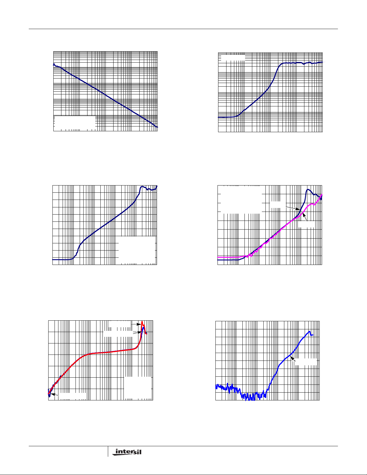
Typical Performance Curves (Continued)
ISL28190, ISL28290
1M
100k
10k
1k
100
OUTPUT IMPEDANCE (Ω)
V+ = 5V, 3V
SOURCE
= 1V
P-P
1M
FREQUENCY (Hz)
10M
100M 1G
V
10
100k
FIGURE 5. DISABLED OUTPUT IMPEDANCE vs FREQUENCY
0
-10
-20
-30
-40
-50
-60
CMRR (dB)
CMRR (dB)
-70
-80
-90
-100
-110
1k
10k
100k
FREQUENCY (Hz)
1M
V+ = 5V
= +1
A
V
= 10kΩ
R
L
= 10pF
C
L
= 100mV
V
OUT
10M 100M
P-P
100
V+ = 5V, 3V
10
1
0.1
OUTPUT IMPEDANCE (Ω)
0.01
100k
1M
FREQUENCY (Hz)
10M
100M 1G
FIGURE 6. ENABLED OUTPUT IMPEDANCE vs FREQUENCY
0
V+ = 5V
-10
= +1
A
V
= 10kΩ
R
L
-20
C
= 10pF
-30
-40
-50
PSRR (dB)
-60
-70
-80
-90
1k
V
L
OUT
= 100mV
10k
P-P
FREQUENCY (Hz)
100k
PSRR-
1M
PSRR+
10M 100M
FIGURE 7. CMRR vs FREQUENCY
-10
-20
-30
-40
-50
-60
OFF ISOLATION (dB)
-70
-80
10k 100k
V
P-P
= 10mV
1M
FREQUENCY (Hz)
V
P-P
10M
V
= 1V
P-P
= 100mV
FIGURE 9. OFF ISOLATION vs FREQUENCY
5
V+ = 5V
= +1
A
V
= 10kΩ
R
L
= 10pF
C
L
100M 1G
FIGURE 8. PSRR vs FREQUENCY
-20
-30
-40
-50
-60
-70
-80
-90
CROSSTALK (dB)
-100
-110
-120
10k 100k
1M
FREQUENCY (Hz)
10M
V
= 1V
P-P
100M 1G
FIGURE 10. CHANNEL TO CHANNEL CROSSTALK vs
FREQUENCY
April 13, 2007
FN6247.3

Typical Performance Curves (Continued)
ISL28190, ISL28290
10
1
INPUT VOLTAGE NOISE (nV/√Hz)
0.1
0.1
1 10 100 1k 10k
FREQUENCY (Hz)
FIGURE 11. INPUT REFERRED NOISE VOL TAGE vs
FREQUENCY
5
4
ENABLE INPUT
V+ = 5V
= +1
A
V
R
= 10kΩ
L
= 10pF
C
L
= 1V
V
IN
P-P
3
2
VOLTS (V)
ENABLEDISABLEENABLE
1
OUTPUT
0
-1.00 0.00 1.00 2.00 3.00 4.00
TIME (µs)
FIGURE 13. ENABLE/DISABLE TIMING
100k
1000
100
10
CURRENT NOISE (pA/√Hz)
1
0.1
1 10 100 1k 10k
FREQUENCY (Hz)
100k
FIGURE 12. INPUT REFERRED NOISE CURRENT vs
FREQUENCY
0.08
0.06
0.04
0.02
0
-0.02
SMALL SIGNAL (V)
-0.04
-0.06
-0.08
0 200 400 600 800
V+ = 5V
= +1
A
V
R
= 10kΩ
L
= 10pF
C
L
V
OUT
TIME (ns)
V
V
OUT
IN
V
IN
= 100mV
P-P
FIGURE 14. SMALL SIGNAL STEP RESPONSE RISE AND
FALL TIME
0.6
0.4
0.2
0
-0.2
LARGE SIGNAL (V)
-0.4
-0.6
0 100 200 300 400 500 600 700 800
V+ = 5V
= +1
A
V
= 10kΩ
R
L
= 10pF
C
L
V
OUT
= 1V
P-P
TIME (ns)
V
IN
V
OUT
FIGURE 15. LARGE SIGNAL STEP RESPONSE RISE AND
FALL TIME
6
6.0
n = 50
5.5
5.0
4.5
4.0
CURRENT (mA)
3.5
3.0
2.5
MEDIAN
-40 -20 0 20 40 60 80 100 120
TEMPERATURE (°C)
MAX
MIN
FIGURE 16. SUPPLY CURRENT vs TEMPERA TURE V
ENABLED. R
= INF
L
= ±2.5V
S
FN6247.3
April 13, 2007

Typical Performance Curves (Continued)
ISL28190, ISL28290
600
n = 50
500
400
300
200
100
0
VIO (µV)
-100
-200
-300
-400
-500
-40 -20 0 20 40 60 80 100 120
MAX
MEDIAN
MIN
TEMPERATURE (°C)
FIGURE 17. VIO vs TEMPERATURE VS = ±2.5V
-9
n = 50
-10
-11
(µA)
-12
BIAS-
I
-13
MEDIAN
MAX
MIN
-9
n = 50
-10
-11
(µA)
-12
MEDIAN
BIAS+
I
-13
-14
-15
-40-200 20406080100120
TEMPERATURE (°C)
FIGURE 18. I
800
n = 50
600
400
200
IOS (nA)
MEDIAN
0
vs TEMPERATURE VS = ±2.5V
BIAS+
MAX
MIN
MAX
-14
-15
-40 -20 0 20 40 60 80 100 120
TEMPERATURE (°C)
FIGURE 19. I
140
n = 50
130
120
110
100
CMRR (dB)
MEDIAN
90
80
70
-40-200 20406080100120
vs TEMPERATURE VS = ±2.5V
BIAS-
MAX
MIN
TEMPERATURE (°C)
FIGURE 21. CMRR vs TEMPERATURE VCM = 3.8V ,
V
= ±2.5V
S
-200
MIN
-400
-40 -20 0 20 40 60 80 100 120
TEMPERATURE (°C)
FIGURE 20. IOS vs TEMPERATURE V
83
n = 50
82
81
80
79
PSRR (dB)
78
77
76
75
-40 -20 0 20 40 60 80 100 120
MEDIAN
TEMPERATURE (°C)
MAX
MIN
= ±2.5V
S
FIGURE 22. PSRR vs TEMPERATURE ±1.5V TO ±2.5V
7
FN6247.3
April 13, 2007

Typical Performance Curves (Continued)
ISL28190, ISL28290
4.982
4.980
4.978
4.976
4.974
(V)
4.972
OUT
4.970
V
4.968
4.966
4.964
4.962
FIGURE 23. POSITIVE V
MEDIAN
MIN
-40 -20 0 20 40 60 80 100 120
TEMPERATURE (°C)
vs TEMPERA TURE RL = 1k
= ±2.5V
OUT
V
S
Pin Descriptions
ISL28190
(6 Ld SOT-23)
412 (A)
ISL28190
(6 Ld μTDFN)
ISL28290
(10 Ld MSOP)
8 (B)
MAX
n = 50
ISL28190
(10 Ld μTDFN)
1 (A)
7 (B)
50
n = 50
45
40
35
MEDIAN
(mV)
30
OUT
V
25
20
15
10
-40-200 20406080100120
MIN
FIGURE 24. NEGATIVE V
V
= ±2.5V
S
MAX
TEMPERATURE (°C)
vs TEMPERATURE RL = 1k
OUT
PIN
NAME FUNCTION EQUIVALENT CIRCUIT
IN- Inverting input
V+
333 (A)
7 (B)
2 (A)
6 (B)
IN+ Non-inverting
input
2 2 4 3 V- Negative sup p ly
141 (A)
9 (B)
10 (A)
8 (B)
OUT Output
6 6 10 9 V+ Positive supply
555 (A)
6 (B)
4 (A)
5 (B)
ENABLE
Enable BAR pin
internal pull-down;
Logic “1” selects
the disabled state;
Logic “0” selects
the enabled state.
IN+IN-
V-
Circuit 1
(See circuit 1)
V+
OUT
V-
Circuit 2
V+
ENABLE
V-
Circuit 3
8
FN6247.3
April 13, 2007

ISL28190, ISL28290
Applications Information
Product Description
The ISL28190 and ISL28290 are voltage feedback operational
amplifier designed for communication and imaging applications
requiring very low voltage and current noise. Both parts feature
low distortion while drawing moderately low supply current. The
ISL28190 and ISL28290 use a classical voltage-feedback
topology which allows them to be used in a variety of
applications where current-feedback amplifiers are not
appropriate because of restrictions placed upon the feedback
element used with the amplifier.
Enable/Power-Down
The ISL28190 and ISL28290 amplifiers are disabled by
applying a voltage greater than 2V to the ENABLE
respect to the V- pin. In this condition, the output(s) will be in
a high impedance state and the amplifier(s) current will be
reduced to 13µA/Amp. By disabling the part, multiple parts
can be connected together as a MUX. The outputs are tied
together in parallel and a channel can be selected by the
ENABLE
down. If left open, the ENABLE
pin. The ENABLE pin also has an internal pull
pin will pull to the negative
rail and the device will be enabled by default.
Input Protection
All input terminals have internal ESD protection diodes to both
positive and negative supply rails, limiting the input volt age to
within one diode beyond the supply rails. Both parts have
additional back-to-back diodes across the input terminals (as
shown in Figure 25). In pulse applications where the input
Slew Rate exceeds the Slew Rate of the amplifier, the
possibility exists for the input protection diodes to become
forward biased. This can cause excessive input current and
distortion at the outputs. If overdriving the inputs is necessary,
the external input current must never exceed 5mA. An
external series resistor may be used to limit the current as
shown in Figure 25.
-
R
+
FIGURE 25. LIMITING THE INPUT CURRENT TO LESS THAN
FIGURE 23. LIMITING THE INPUT CURRENT TO LESS THAN
5mA
5mA
Using Only One Channel
The ISL28290 is a Dual channel op-amp. If the application
only requires one channel when using the ISL28290, the
user must configure the unused channel to prevent it from
oscillating. Oscillation can occur if the input and output pins
are floating. This will result in higher than expected supply
currents and possible noise injection into the channel being
used. The proper way to prevent this oscillation is to short
pin, with
the output to the negative input and ground the positive input
(as shown in Figure 26).
-
+
FIGURE 26. PREVENTING OSCILLATIONS IN UNUSED
CHANNELS
Current Limiting
The ISL28190 and ISL28290 have no internal currentlimiting circuitry. If the output is shorted, it is possible to
exceed the Absolute Maximum Rating for output current or
power dissipation, potentially resulting in the destruction of
the device. This is why output short circuit current is
specified and tested with R
= 10Ω.
L
Power Dissipation
It is possible to exceed the +125°C maximum junction
temperatures under certain load and power-supply
conditions. It is therefore important to calculate the
maximum junction temperature (T
to determine if power supply voltages, load conditions, or
package type need to be modified to remain in the safe
operating area. These parameters are related as follows:
T
JMAXTMAXθJA
xPD
()+=
MAXTOTAL
where:
•P
DMAXTOTAL
is the sum of the maximum power
dissipation of each amplifier in the package (PD
•PD
PD
whereT
for each amplifier can be calculated as follows:
MAX
MAX
2*VSI
= Maximum ambient temperature
MAX
( - V
SMAXVS
• θJA = Thermal resistance of the package
•PD
•V
•I
•V
= Maximum power dissipation of 1 amplifier
MAX
= Supply voltage
S
= Maximum supply current of 1 amplifier
MAX
OUTMAX
= Maximum output voltage swing of the
application
= Load resistance
•R
L
) for all applications
JMAX
V
----------------------------
)
OUTMAX
×+×=
MAX
OUTMAX
R
L
)
9
FN6247.3
April 13, 2007

ISL28190, ISL28290
Power Supply Bypassing and Printed Circuit
Board Layout
As with any high frequency device, good printed circuit
board layout is necessary for optimum performance. Low
impedance ground plane construction is essential. Surface
mount components are recommended, but if leaded
components are used, lead lengths should be as short as
possible. The power supply pins must be well bypassed to
reduce the risk of oscillation. The combination of a 4.7µF
tantalum capacitor in parallel with a 0.01µF capacitor has
been shown to work well when placed at each supply pin.
For good AC performance, parasitic capacitance should be
kept to a minimum, especially at the inverting input. When
ground plane construction is used, it should be removed
from the area near the inverting input to minimize any stray
capacitance at that node. Carbon or Metal-Film resistors are
acceptable with the Metal-Film resistors giving slightly less
peaking and bandwidth because of additional series
inductance. Use of sockets, particularly for the SO package,
should be avoided if possible. Sockets add parasitic
inductance and capacitance which will result in additional
peaking and overshoot.
10
FN6247.3
April 13, 2007

ISL28190, ISL28290
SOT-23 Package Family
e1
A
6
N
E1
2 3
0.15 DC
2X
5
e
B
NX
0.15 A-BC
2X
C
SEATING
PLANE
0.10 C
NX
MDP0038
SOT-23 PACKAGE FAMILY
D
SYMBOL
4
A 1.45 1.45 MAX
A1 0.10 0.10 ±0.05
A2 1.14 1.14 ±0.15
E
b 0.40 0.40 ±0.05
c 0.14 0.14 ±0.06
321
0.20
b
M
0.20 C
2X
DC A-B
D 2.90 2.90 Basic
E 2.80 2.80 Basic
E1 1.60 1.60 Basic
e 0.95 0.95 Basic
e1 1.90 1.90 Basic
L 0.45 0.45 ±0.10
L1 0.60 0.60 Reference
N 5 6 Reference
1 3
D
NOTES:
1. Plastic or metal protrusions of 0.25mm maximum per side are not
included.
A2
2. Plastic interlead protrusions of 0.25mm maximum per side are not
included.
3. This dimension is measured at Datum Plane “H”.
A1
4. Dimensioning and tolerancing per ASME Y14.5M-1994.
5. Index area - Pin #1 I.D. will be located within the indicated zone
(SOT23-6 only).
6. SOT23-5 version has no center lead (shown as a dashed line).
MILLIMETERS
TOLERANCESOT23-5 SOT23-6
Rev. F 2/07
(L1)
A
c
L
0°
GAUGE
PLANE
+3°
-0°
H
0.25
11
FN6247.3
April 13, 2007

ISL28190, ISL28290
Ultra Thin Dual Flat No-Lead Plastic Package (UTDFN)
PIN 1
REFERENCE
2X
0.15 C
2X
6X
E
64
13
0.15 C
TOP VIEW
46
D2
31
BOTTOM VIEW
0.10 C
0.08 C
SIDE VIEW
1.00 REF
CO.2
E2
A
B
D
e
L
DAP SIZE 1.30 x 0.76
b6X
0.10 CAB
DETAIL A
C
A3
SEATING
PLANE
A
L6.1.6x1.6A
6 LEAD ULTRA THIN DUAL FLAT NO-LEAD PLASTIC PACKAGE
MILLIMETERS
A1
SYMBOL
A
A1
A3
b
D
0.45 0.50 0.55
- - 0.05
0.127 REF
0.15 0.20 0.25
1.55 1.60 1.65
NOTESMIN NOMINAL MAX
-
-
-
-
4
D2 0.40 0.45 0.50 -
E
E2
e
L
M
NOTES:
1.55 1.60 1.65
0.95 1.00 1.05
0.50 BSC
0.25 0.30 0.35
4
-
-
-
Rev. 1 6/06
1. Dimensions are in mm. Angles in degrees.
2. Coplanarity applies to the exposed pad as well as the terminals.
Coplanarity shall not exceed 0.08mm.
3. Warpage shall not exceed 0.10mm.
4. Package length/package width are considered as special
characteristics.
5. JEDEC Reference MO-229.
6. For additional information, to assist with the PCB Land Pattern
Design effort, see Intersil Technical Brief TB389.
0.127±0.008
A1
0.50
1.00
1.25
DETAIL A
0.25
0.45
0.30
LAND PATTERN
0.127 +0.058
-0.008
TERMINAL THICKNESS
1.00
2.00
6
12
FN6247.3
April 13, 2007

ISL28190, ISL28290
Ultra Thin Quad Flat No-Lead Plastic Package (UTQFN)
INDEX AREA
2X
0.10 C
0.05 C
SEATING PLANE
NX (b)
5
SECTION "C-C"
6
2X
0.10 C
0.10 C
A
A1
(DATUM A)
PIN #1 ID
L1
(A1)
N
TOP VIEW
SIDE VIEW
7
BOTTOM VIEW
CC
D
A
B
L10.1.8x1.4A
10 LEAD ULTRA THIN QUAD FLAT NO-LEAD PLASTIC
PACKAGE
E
SYMBOL
21
A 0.45 0.50 0.55 -
MILLIMETERS
NOTESMIN NOMINAL MAX
A1 - - 0.05 A3 0.127 REF -
b 0.15 0.20 0.25 5
D 1.75 1.80 1.85 -
C
E 1.35 1.40 1.45 e 0.40 BSC L 0.35 0.40 0.45 -
L1 0.45 0.50 0.55 -
N102
Nd 2 3
NX L
21
5
5
NX b
10X
0.10 M C A B
0.05 M C
(DATUM B)
Ne 3 3
θ
0-12
Rev. 3 6/06
NOTES:
1. Dimensioning and tolerancing conform to ASME Y14.5-1994.
4
2. N is the number of terminals.
e
3. Nd and Ne refer to the number of terminals on D and E side,
respectively.
4. All dimensions are in millimeters. Angles are in degrees.
5. Dimension b applies to the metallized terminal and is measured
C
L
between 0.15mm and 0.30mm from the terminal tip.
6. The configuration of the pin #1 identifier is optional, but must be
located within the zone indicated. The pin #1 identi fier may be
L
either a mold or mark feature.
7. Maximum package warpage is 0.05mm.
e
TERMINAL TIP
8. Maximum allowable burrs is 0.076mm in all directions.
9. JEDEC Reference MO-255.
10. For additional information, to assist with the PCB Land Pattern
Design effort, see Intersil Technical Brief TB389.
1.80
1.00
0.50
0.20
2.20
1.00
0.60
0.40
10
LAND PATTERN
13
0.20
0.40
FN6247.3
April 13, 2007

Mini SO Package Family (MSOP)
M
C
SEATING
PLANE
0.10 C
N LEADS
c
0.25 C A B
E1E
B
L1
SEE DETAIL "X"
D
N
1
e
b
A
(N/2)+1
PIN #1
I.D.
(N/2)
H
M
0.08 C A B
A
ISL28190, ISL28290
MDP0043
MINI SO PACKAGE FAMILY
SYMBOL
A 1.10 1.10 Max. A1 0.10 0.10 ±0.05 A2 0.86 0.86 ±0.09 -
b 0.33 0.23 +0.07/-0.08 -
c 0.18 0.18 ±0.05 -
D 3.00 3.00 ±0.10 1, 3
E 4.90 4.90 ±0.15 E1 3.00 3.00 ±0.10 2, 3
e 0.65 0.50 Basic -
L 0.55 0.55 ±0.15 L1 0.95 0.95 Basic -
N 8 10 Reference -
NOTES:
1. Plastic or metal protrusions of 0.15mm maximum per side are not
included.
2. Plastic interlead protrusions of 0.25mm maximum per side are
not included.
3. Dimensions “D” and “E1” are measured at Datum Plane “H”.
4. Dimensioning and tolerancing per ASME Y14.5M-1994.
MILLIMETERS
TOLERANCE NOTESMSOP8 MSOP10
Rev. D 2/07
A2
GAUGE
A1
L
DETAIL X
PLANE
3° ±3°
0.25
All Intersil U.S. products are manufactured, assembled and tested utilizing ISO9000 quality systems.
Intersil Corporation’s quality certifications can be viewed at www.intersil.com/design/quality
Intersil products are sold by description only. Intersil Corporation reserves the right to make changes in circuit design, software and/or specifications at any time without
notice. Accordingly, the reader is cautioned to verify that data sheets are current before placing orders. Information furnished by Intersil is believed to be accurate and
reliable. However, no responsibility is assumed by Intersil or its subsidiaries for its use; nor for any infringements of patents or other rights of third parties which may result
from its use. No license is granted by implicat ion or oth erwise u nde r any p a tent or p at ent r ights of Intersil or its subsidiari es.
For information regarding Intersil Corporation and its products, see www.intersil.com
14
FN6247.3
April 13, 2007
 Loading...