

Page 1

Application Note 1480
ISL28133ISENSEV1Z Evaluation Board User’s Guide
The ISL28133ISENSEV1Z evaluation board contains a
complete precision current sense amplifier using the
ISL28133 chopper amplifier in a high side, low side of floating
supply current sense application.
The advantages of the ISL28133 in this application include very
low offset voltage (2µV typical) and offset drift (0.07µV/°C),
rail-to-rail input and output and low power consumption (18µA
typical). These features provide a very high degree of precision
for use in 5V, low power applications.
Reference Documents
• ISL28133 Data Sheet (FN6560)
Evaluation Board Key Features
The ISL28133ISENSEV1Z operates from a single 1.65VDC to
+5.5VDC supply. The current sense function is configured as a
single stage, balanced input, trans-impedance amplifier. A
0.1Ω 0.1% current sense resistor is used convert the incoming
current to a voltage which is applied to a precision differential
amplifier with a gain of 100. The overall current to voltage
transfer ratio is 10V/A, and a bidirectional current range of
±0.25A is achieved when operating from a +5V supply, using a
2.5V reference voltage (V
achieves a total full scale offset error of 0.038% (when a
precision external reference is used) and approximately 0.15%
using the internal 0.1% resistors.
The total current draw from the amplifier power is less than
35µA and the total leakage current from the current sense
input is less than 3µA.
). At +25°C, the ISL28133
REF
High speed current sensing may involve filtering repetitive
current transients with high peak to average values. In these
cases, limiting these transient even further will improve
amplifier response and overload settling time. The optional
Schottky diode transient clamp D2 reduces transients let
through by the common mode clamp from 6V down to
~ ±0.3V, which improves overload recovery time. Capacitors
C7 and C9 provide common mode noise filtering and capacitor
C8 can be used to filter the current sense signal.
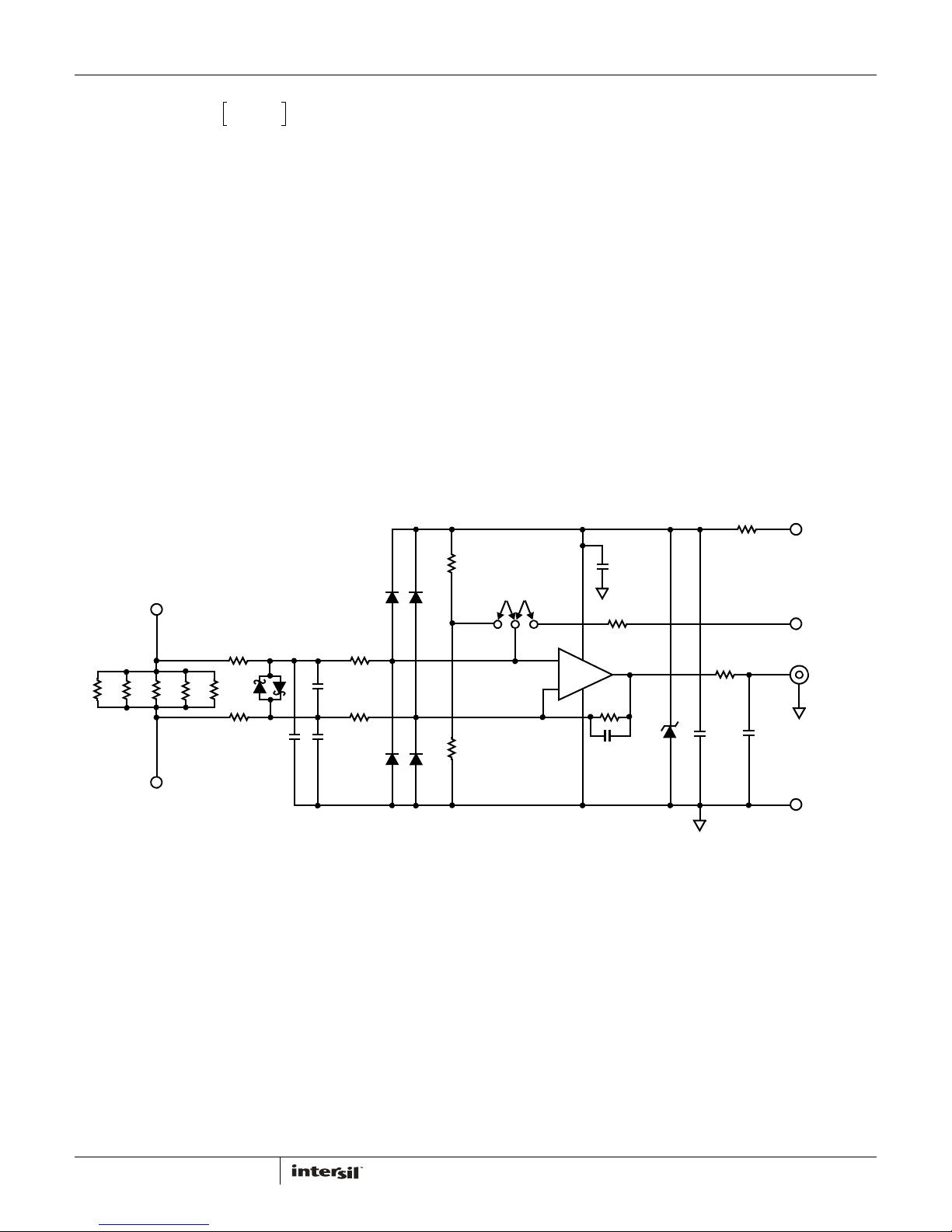
Current Sense Gain Equations
The current sense amplifier in Figure 1 forms a
trans-impedance amplifier whose gain is in units of V/A and is
determined by the ratios of resistor pairs. R11:R8 and R14:
R9. Resistor R11 is set equal to R14 and R8 is set equal to R9.
This matching cancels the input offset voltage errors caused
by the op amp input bias currents, leaving behind only the
offset voltage errors caused by the ISL28133 input offset
SENSE
=
OS
).
to V
10
DC transfer function is given by Equation 1:
OUT
×
V
---
A
R14
---------- -
+=
× V
R9
SENSE
REF
is 0.1Ω for a trans-impedance
(EQ. 1)
(EQ. 2)
current (I
The I
V
OUTISENSERSENSE
where:
R11 = R14 and R6 + R8 = R7 + R9
On the evaluation board, the R12, R9 resistor ratio is 100:1
(499kΩ: 4.9kΩ), and R
gain given by Equation 2:
V
SENSE
------------------- -
I
SENSE
Power Supply and Protection Features
External power connections are made through the +V, and
ground jacks. The single supply input is overvoltage protected
using a series 100Ω resistor and a 5.6V zener diode (D1).
Reverse polarity protection uses the 100Ω resistor and two
protection diode pairs (D3, D4). These also provide input
common mode voltage protection to the op amp.
Input Protection Clamp Options
Included on the evaluation board are optional input protection
circuits that illustrate the best methods to limit input common
mode and differential transient voltage spikes in exposed or
electrically hazardous applications. The ISL28133 can handle
input common mode and differential transients to a diode drop
beyond the rails, or to a range of -0.5V to +5.5V when operating
from a single 5V supply.
Clamp diodes D3A, B, D4A, B and input resistors R6, R7, R8,
R9 form a current limiting, 6V common mode and differential
voltage clamp. This clamp provides sufficient protection for the
ISL28133 for common mode fault voltages far beyond the
power supply rails. These diodes also provide the same 6V
protection against large differential transients.
Input Range and Offset Error Analysis
The ISL28133 output swings from rail-to-rail, and the evaluation
board has a bi-directional output range of V
operated from a +5V supply and V
is set to VS/2. The
REF
evaluation board contains a jumper-selectable, internal V
reference or an external reference (V
REF
+2.5, the full scale output range is 0 ±0.25A.
The very low offset voltage (±8µV +25°C max) and offset
current (300pA +25°C max) of the ISL28133 enable the use
of very high values resistors for low current consumption while
maintaining excellent precision in battery operated circuits.
The total offset voltage contribution of the ISL28133 is the
sum of the input offset voltage (V
) and the offset voltage
OS
produced by the input offset current (IOS) through the gain
resistors and using the evaluation board resistor values and
the data sheet maximum +25°C V
gives the total input
OS
offset voltage as shown in Equations 3, 4 and 5:
R14 R9×
⎛⎞
-------------------------
V
OS Total()
IOS
×
⎝⎠
R14 R9+
VOS+=
±2.5V when
REF
pin). With V
REF
/2
S
set to
(EQ. 3)
July 18, 2011
AN1480.2
1
CAUTION: These devices are sensitive to electrostatic discharge; follow proper IC Handling Procedures.
1-888-INTERSIL or 1-888-468-3774 | Copyright Intersil Americas Inc. 2011. All Rights Reserved
Intersil (and design) is a trademark owned by Intersil Corporation or one of its subsidiaries.
All other trademarks mentioned are the property of their respective owners.
Page 2
Application Note 1480
V
OS Total()
V
OS Total()
⎛⎞
3e 10
⎝⎠
3e 10 4950×–()= 8μ V9.5μV=+
R14 R9×
-------------------------
×–
R14 R9+
8μ V+=
(EQ. 4)
(EQ. 5)
Multiplying the ISL28133 input offset voltage by the amplifier
gain allows the input offset error to be expressed as a percent of
full scale output voltage.
R14
---------- -
×
V
OS
R9
(EQ. 6)
2.5V±
% F.S. Error
⎛⎞
⎝⎠
------------------------------------ -
= 0.038%±=
Using the Evaluation Board
The evaluation board has separate connections for the amplifier
power supply, an output zero reference (V
sense terminals. The correct inter-connection between the ISENSE terminals and the V
terminals are needed to
REF
implement the different types of current sense configurations.
The I-SENSE + and I-SENSE - connections to the measured circuit
determine the polarity of the amplifier output voltage.
Establishing a current flow from the I-SENSE + to I-SENSE causes the output voltage to increase in proportion to the input
current. Reversing the I-SENSE current flow reverses the output
polarity.
I-SENSE+
R6
10Ω
R1
DNPR2DNPR30.1R4DNPR5DNP
R7
10Ω
D2
C7
1nF
),and the current
REF
D3A
R8
4.99k
C8
10nF
R9
4.99k
C9
1nF
D3B D4B
D4A
The voltage applied to the V
pin defines the amplifier output
REF
zero current level, and must be between 0V and +5V. For
bi-directional current sensing, a reference midway between the
ground and the supply voltage will maximize the output span. For
example, a V
= +2.5V would be the best choice for +5V power
REF
supply. The jumper selectable internal voltage divider is provided
for this internal reference. The +2.5V will establish an output
current scale setting 0A = +2.5V, but the accuracy is determined
by the voltage divider accuracy (0.1% resistors on the evaluation
board). Connecting the jumper to the external reference position
enables an external reference source to be used.
Figure 2 shows the connections to implement a high side,
bi-directional current sense with the ability to monitor the
charging current. Figure 3 shows the connection for
uni-directional ground referenced current sensing. The ISL28133
maintains precision performance from rail-to-rail making
precision ground-side sensing possible.
R15
1.65V TO +5.5V
R13
0
C2
4.7µF
100
C10
OPEN
R12A, B
1M
VS/2
REFERENCE
R10A, B
1M
JUMPER
EXT
REFERENCE
3
+
ISL28133
4
-
C4
1nF
R11
499k
5
V+
1
V-
R14
2
499k
D1
5.6V
C20
OPEN
V
S
V
REF
I
SENSE
OUT
I-SENSE-
FIGURE 1. ISL28133 DIFFERENTIAL CURRENT SENSE AMPLIFIER
2
GND
AN1480.2
July 18, 2011
Page 3

CONNECT TO
EXTERNAL
POWER
Application Note 1480
CONNECT TO
BATTERY
POWER
V
S
1.65V TO +5.5V
I-SENSE+
+
JUMPER
EXT
REFERENCE
V
REF
VS/2
REFERENCE
R
SENSE
LOAD
CURRENT
FLOW
I-SENSE-
V
= +2.5V ±2.5V
OUT
I
SENSE
V
= +2.5V
REF
FOR
= 0A ±0.25A
CHARGING
CURRENT
GND
V
I
SENSE
OUT
REF
FIGURE 2. CURRENT SENSE FOR HIGH-SIDE BI-DIRECTIONAL RE-CHARGEABLE BATTERY SUPPLY
CONNECT TO
BATTERY
EXTERNAL
POWER
1.65V TO +5.5V
V
S
1.65V TO +5.5V
POWER
I-SENSE+
-
V
OUT
I
SENSE
V
= 0V
REF
= 0V TO 5V
FOR
= 0A 0.5A
GND
V
I
SENSE
OUT
REF
JUMPER
EXT
REFERENCE
VS/2
REFERENCE
R
SENSE
CURRENT
FLOW
I-SENSE-
FIGURE 3. CURRENT SENSE FOR LOW SIDE UNI-DIRECTIONAL MEASUREMENT
LOAD
0V
TO
+5.5V
3
AN1480.2
July 18, 2011
Page 4

Application Note 1480
ISL28133ISENSEV1Z Components Parts List
DEVICE # DESCRIPTION COMMENTS
C2 CAP-SMD, 0805, 4.7µF, 50V, 10%, X7R, ROHS Power supply decoupling
C4, C7, C9 CAP, SMD, 0603, 1000F, 25V, 10%, X7R, ROHS Power supply decoupling
C8 CAP, SMD, 0603, 0.1µF, 25V, 10%, X7R, ROHS Power supply decoupling
C10, C20 CAP, SMD, 0603, DNP-PLACE HOLDER, ROHS User-selectable capacitors - not populated
D1 Zener Diode ROHS Reverse power protection
D2- D4 DIODE-SCHOTTKY BARRIER, SMD, SOT-23, 3P, 40V, ROHS Reverse power protection
R13 RESISTOR, SMD, 0603, 0Ω, 1/16W, 0.1%, TF, ROHS 0Ω user selectable resistors
R1- R5 RES, SMD, 0805, 0.1Ω, 1/10W, 0.1%, TF, ROHS Current sense resistors
R6, R7 RES, SMD, 0805, 10Ω, 1/10W, 0.1%, TF, ROHS Protection resistors
R15 RES, SMD, 0805, 100Ω, 1/10W, 0.1%, TF, ROHS Protection resistors
R8, R9 RES, SMD, 0805, 4.99kΩ, 1/10W, 0.1%, TF, ROHS 0Ω user selectable resistors
R11, R14, R10A, R10B, R12A, R12B RES, SMD, 0805, 499kΩ, 1/10W, 0.1%, TF, ROHS Gain and other user selectable resistors
U1 (ISL28133FHZ-T7) IC-5 MHz, RRIO OP AMP, SOT23_5, ROHS
R1, R2, R4, R5 RES, SMD, 0805, DNP Optional sense resistors
4
AN1480.2
July 18, 2011
Page 5

Application Note 1480
ISL28133ISENSEV1Z Schematic Diagram
R1
DNP
R2
I-SENSE + I-SENSE
J4 J5
R6
10
C7
1000pF
DNP
R3
0.10
R4
DNP
R5
DNP
C8
0.01µF
D2
-
R7
10
C9
1000pF
V-REF
J1
R11
499k
R10B
499k
R10A
499k
R12B
499k
R12A
499k
R8
4.99k
D3
C20
OPEN
R14
499k
1
2
ISL28133
3
SOT23_5
4.7µF
1000pF
C2
C4
D1
U2
R9
4.99k
D4
R13
0
C10
OPEN
5
4
J6
I-SENSE
OUT
5
J2
GND
R15
100
J3
VS1+
AN1480.2
July 18, 2011
Page 6

Application Note 1480
FIGURE 4. ISL28133ISENSEV1Z TOP VIEW
Intersil Corporation reserves the right to make changes in circuit design, software and/or specifications at any time without notice. Accordingly, the reader is
cautioned to verify that the Application Note or Technical Brief is current before proceeding.
For information regarding Intersil Corporation and its products, see www.intersil.com
6
AN1480.2
July 18, 2011
 Loading...