

Page 1
Single, Dual, Quad General Purpose Micropower, RRIO
Operational Amplifier
ISL28113, ISL28213, ISL28413
The ISL28113, ISL28213, and ISL28413 are single, dual, and
quad channel general purpose micropower, rail-to-rail input and
output operational amplifiers with supply voltage range of 1.8V
to 5.5V. Key features are a low supply current of 130µA
maximum per channel at room temperature, a low bias current
and a wide input voltage range, which enables the ISL28x13
devices to be excellent general purpose op-amps for a wide range
of applications.
The ISL28113 is available in the SC70-5 and SOT23-5 packages,
the ISL28213 is in the MSOP8, SOIC8, SOT23-8 packages, and
the ISL28413 is in the TSSOP14, SOIC14 packages. All devices
operate over the extended temperature range of -40°C to
+125°C.
Related Literature
•See AN1519 for “ISL28213/14SOICEVAL2Z Evaluation Board
User’s Guide”
•See AN1520
Board User’s Guide”
•See AN1542
User’s Guide”
for “ISL28113/14SOT23EVAL1Z Evaluation
for “ISL28213/14MSOPEVAL2Z Evaluation Board
Features
• Low Current Consumption. . . . . . . . . . . . . . . . . . . . . . . . . . 130µA
• Wide Supply Range . . . . . . . . . . . . . . . . . . . . . . . . . . 1.8V to 5.5V
• Gain Bandwidth Product . . . . . . . . . . . . . . . . . . . . . . . . . . . . 2MHz
• Input Bias Current . . . . . . . . . . . . . . . . . . . . . . . . . . . . 20pA, Max.
• Operating Temperature Range. . . . . . . . . . . . .-40°C to +125°C
•Packages
- ISL28113 (Single) . . . . . . . . . . . . . . . . . . . . . SC70-5, SOT23-5
- ISL28213 (Dual). . . . . . . . . . . . . . . . MSOP8, SOIC8, SOT23-8
- ISL28413 (Quad) . . . . . . . . . . . . . . . . . . . . . SOIC14, TSSOP14
Applications
• Power Supply Control/Regulation
• Process Control
• Signal Gain/Buffers
• Active Filters
• Current Shunt Sensing
•Trans-impedance Amps
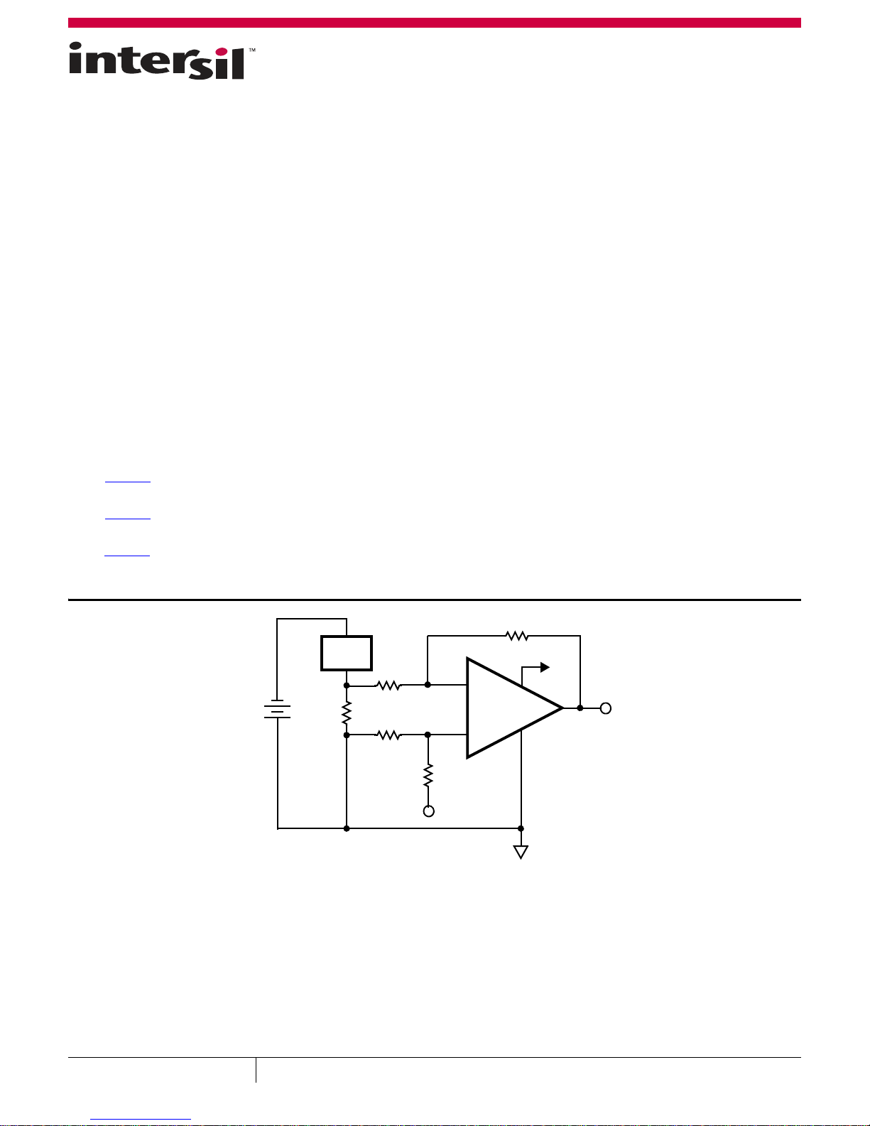
RF
LOAD
RIN-
RSENSE
SINGLE-SUPPLY, LOW-SIDE CURRENT SENSE AMPLIFIER
10kΩ
RIN+
10kΩ
VREF
FIGURE 1. TYPICAL APPLICATION
IN-
IN+
RREF+
100kΩ
100kΩ
-
ISL28x13
+
+5V
V+
V-
GAIN = 10
VOUT
June 9, 2011
FN6728.5
1
CAUTION: These devices are sensitive to electrostatic discharge; follow proper IC Handling Procedures.
1-888-INTERSIL or 1-888-468-3774
Intersil (and design) is a trademark owned by Intersil Corporation or one of its subsidiaries.
All other trademarks mentioned are the property of their respective owners.
|Copyright Intersil Americas Inc. 2009-2011. All Rights Reserved
Page 2
ISL28113, ISL28213, ISL28413
Ordering Information
PART NUMBER
(Notes 2, 3)
PART
MARKING
PACKAGE
(Pb-Free)
PKG.
DWG. #
ISL28113FEZ-T7 (Note 1) BJA 5 Ld SC-70 P5.049
ISL28113FEZ-T7A (Note 1) BJA 5 Ld SC-70 P5.049
ISL28113FHZ-T7 (Note 1) BCYA 5 Ld SOT-23 P5.064A
ISL28113FHZ-T7A (Note 1) BCYA 5 Ld SOT-23 P5.064A
ISL28213FUZ 8213Z 8 Ld MSOP M8.118A
ISL28213FUZ-T7 (Note 1) 8213Z 8 Ld MSOP M8.118A
ISL28213FBZ 28213 FBZ 8 Ld SOIC M8.15E
ISL28213FBZ-T7 (Note 1) 28213 FBZ 8 Ld SOIC M8.15E
ISL28213FBZ-T13 (Note 1) 28213 FBZ 8 Ld SOIC M8.15E
Coming Soon
ISL28213FHZ-T7 (Note 1) TBD 8 Ld SOT-23 P8.064
Coming Soon
ISL28213FHZ-T7A (Note 1) TBD 8 Ld SOT-23 P8.064
ISL28413FVZ 28413 FVZ 14 Ld TSSOP MDP0044
ISL28413FVZ-T7 (Note 1) 28413 FVZ 14 Ld TSSOP MDP0044
ISL28413FVZ-T13 (Note 1) 28413 FVZ 14 Ld TSSOP MDP0044
ISL28413FBZ 28413 FBZ 14 Ld SOIC MDP0027
ISL28413FBZ-T7 (Note 1) 28413 FBZ 14 Ld SOIC MDP0027
ISL28413FBZ-T13 (Note 1) 28413 FBZ 14 Ld SOIC MDP0027
ISL28113SOT23EVAL1Z Evaluation Board
ISL28213MSOPEVAL2Z Evaluation Board
ISL28213SOICEVAL2Z Evaluation Board
Coming Soon
Evaluation Board
ISL28413TSSOPEVAL1Z
NOTES:
1. Please refer to TB347
for details on reel specifications.
2. These Intersil Pb-free plastic packaged products employ special Pb-free material sets, molding compounds/die attach materials, and 100% matte
tin plate plus anneal (e3 termination finish, which is RoHS compliant and compatible with both SnPb and Pb-free soldering operations). Intersil
Pb-free products are MSL classified at Pb-free peak reflow temperatures that meet or exceed the Pb-free requirements of IPC/JEDEC J STD-020.
3. For Moisture Sensitivity Level (MSL), please see device information page for ISL28113
see Techbrief TB363
.
, ISL28213, ISL28413. For more information on MSL please
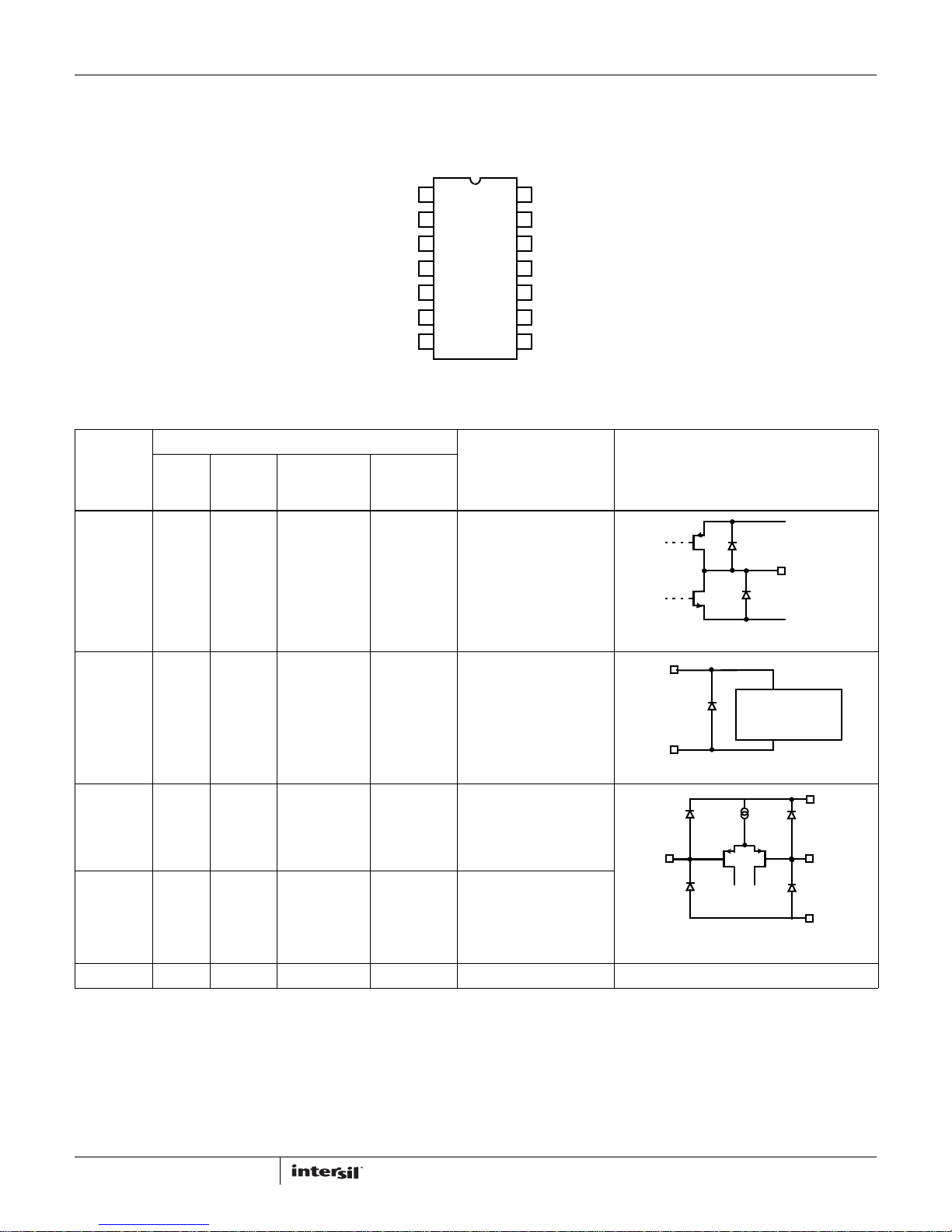
Pin Configurations
ISL28113
(5 LD SC-70)
TOP VIEW
+
IN+
V
IN-
1
-
2
S
354
V
S
OUT
2
OUT
V
IN+
-
S
ISL28113
(5 LD SOT-23)
TOP VIEW
1
2
354
(8 LD MSOP, 8 LD SOIC, 8 LD SOT-23)
ISL28213
TOP VIEW
+
V
S
IN-
OUT_A
IN-_A
IN+_A
V
S
1
2
3
45
-
8
7
6
+
V
S
OUT_B
IN-_B
IN+_B
FN6728.5
June 9, 2011
Page 3
ISL28113, ISL28213, ISL28413
V
Pin Configurations (Continued)
(14 LD TSSOP, 14 LD SOIC)
ISL28413
TOP VIEW
OUT_A
OUT_B
IN-_A
IN+_A
V
S
IN+_B
IN-_B
1
2
3
+
4
5
6
7
Pin Descriptions
PIN NUMBER
8 LD MSOP,
8LD SOIC,
8LDSOT-23
1
7
PIN NAME
OUT
OUT_A
OUT_B
5 LD
SC-70
5 LD
SOT-23
41
OUT_C
OUT_D
VS- 2 2 4 11 Negative supply voltage
14 LD TSSOP,
14 LD SOIC
1
7
8
14
DESCRIPTION
Output
14
13
12
11
10
9
8
OUT_D
IN-_D
IN+_D
V
-
S
IN+_C
IN-_C
OUT_C
+
OUT
V-
CIRCUIT 1
V+
IN+
IN+_A
IN+_B
IN+_C
IN+_D
ININ-_A
IN-_B
IN-_C
IN-_D
V
+ 5 5 8 4 Positive supply voltage See “CIRCUIT 2”
S
13
34
3
5
3
5
10
12
2
6
2
6
9
13
Positive Input
Negative Input
CAPACITIVELY
TRIGGERED
ESD CLAMP
V-
CIRCUIT 2
V+
IN+IN-
V-
CIRCUIT 3
3
FN6728.5
June 9, 2011
Page 4
ISL28113, ISL28213, ISL28413
Absolute Maximum Ratings (T
Supply Voltage . . . . . . . . . . . . . . . . . . . . . . . . . . . . . . . . . . . . . . . . . . . . . . 6.5V
Supply Turn-on Voltage Slew Rate . . . . . . . . . . . . . . . . . . . . . . . . . . . . 1V/µs
Differential Input Current . . . . . . . . . . . . . . . . . . . . . . . . . . . . . . . . . . . 20mA
Differential Input Voltage . . . . . . . . . . . . . . . . . . . . . . .V
Input Voltage. . . . . . . . . . . . . . . . . . . . . . . . . . . . . . . . . .V
ESD Rating
Human Body Model . . . . . . . . . . . . . . . . . . . . . . . . . . . . . . . . . . . . . . 4000V
Machine Model
ISL28113, ISL28213 . . . . . . . . . . . . . . . . . . . . . . . . . . . . . . . . . . . . 350V
ISL28413. . . . . . . . . . . . . . . . . . . . . . . . . . . . . . . . . . . . . . . . . . . . . . 400V
Charged Device Model . . . . . . . . . . . . . . . . . . . . . . . . . . . . . . . . . . . . 2000V
CAUTION: Do not operate at or near the maximum ratings listed for extended periods of time. Exposure to such conditions may adversely impact product
reliability and result in failures not covered by warranty.
NOTES:
4. θ
is measured with the component mounted on a high effective thermal conductivity test board in free air. See Tech Brief TB379 for details.
JA
5. For θ
, the “case temp” location is the top of the package.
JC
= +25°C) Thermal Information
A
Thermal Resistance (Typical) θ
5 Ld SC-70 (Notes 4, 5) . . . . . . . . . . . . . . . . 250 N/A
5 Ld SOT-23 (Notes 4, 5) . . . . . . . . . . . . . . . 225 N/A
- 0.5V to V+ + 0.5V
-
- 0.5V to V+ + 0.5V
-
8 Ld MSOP (Notes 4, 5). . . . . . . . . . . . . . . . 180 100
8 Ld SOIC Package (Notes 4, 5) . . . . . . . . . 126 90
8 Ld SOT-23 (Notes 4, TBD) . . . . . . . . . . . . 240 TBD
14 Ld TSSOP Package (Notes 4, 5) . . . . . . 120 40
14 Ld SOIC Package (Notes 4, 5). . . . . . . . 90 50
Ambient Operating Temperature Range. . . . . . . . . . . . . . -40°C to +125°C
Storage Temperature Range . . . . . . . . . . . . . . . . . . . . . . . -65°C to +150°C
Operating Junction Temperature . . . . . . . . . . . . . . . . . . . . . . . . . . . . +125°C
Pb-Free Reflow Profile. . . . . . . . . . . . . . . . . . . . . . . . . . . . . . . .see link below
http://www.intersil.com/pbfree/Pb-FreeReflow.asp
(°C/W) θJC (°C/W)
JA
Electrical Specifications V
the operating temperature range, -40°C to +125°C, unless otherwise specified.
PARAMETER DESCRIPTION CONDITIONS
+ = 5V, VS- = 0V, RL = Open, V
S
= V
/2, TA = +25°C, unless otherwise specified. Boldface limits apply over
CM
S
MIN
(Note 6) TYP
MAX
(Note 6) UNIT
DC SPECIFICATIONS
V
OS
Input Offset Voltage -5 0.5 5 mV
-6 6 mV
TCV
I
OS
I
B
OS
Input Offset Voltage Temperature
-40°C to +125°C 2 10 µV/°C
Coefficient
Input Offset Current 130 pA
Input Bias Current ISL28113 -20 3 20 pA
-100 100 pA
ISL28213, ISL28413 -20 3 20 pA
-50 50 pA
Common Mode Input
- 0.1V +5.1V V
Voltage Range
Z
IN
C
IN
Input Impedance 10
Input Capacitance 1 pF
12
CMRR Common Mode Rejection Ratio VCM = -0.1V to 5.1V 72 dB
-40°C to +125°C 70 dB
PSRR Power Supply Rejection Ratio V
= 1.8V to 5.5V 71 dB
S
-40°C to +125°C 70 dB
V
OH
Output Voltage Swing, High RL = 10kΩ 4.985 4.993 V
4.98 V
V
OL
Output Voltage Swing, Low RL = 10kΩ 13 15 mV
20 mV
V
+
Supply Voltage 1.8 5.5 V
Ω
4
FN6728.5
June 9, 2011
Page 5
ISL28113, ISL28213, ISL28413
Electrical Specifications V
the operating temperature range, -40°C to +125°C, unless otherwise specified.
+ = 5V, VS- = 0V, RL = Open, V
S
= V
/2, TA = +25°C, unless otherwise specified. Boldface limits apply over
CM
S
(Continued)
MIN
PARAMETER DESCRIPTION CONDITIONS
I
I
I
S
SC+
SC-
Supply Current per Amplifier RL = OPEN 90 130 µA
Output Source Short Circuit Current RL = 10Ω to V- -22 mA
Output Sink Short Circuit Current RL = 10Ω to V+ 16 mA
(Note 6) TYP
AC SPECIFICATIONS
GBWP Gain Bandwidth Product VS = ±2.5V
A
= 100, RF = 100kΩ,
V
R
=1kΩ, RL = 10kΩ to V
Peak-to-Peak Input Noise Voltage VS = ±2.5V
e
N VP-P
e
N
Input Noise Voltage Density VS = ±2.5V
G
f = 0.1Hz to 10Hz
CM
f = 1kHz
i
N
C
in
Input Noise Current Density VS = ±2.5V
f = 1kHz
Differential Input Capacitance VS = ±2.5V
Common Mode Input Capacitance 1.3 pF
f = 1MHz
TRANSIENT RESPONSE
SR Slew Rate 20% to 80% V
t
, tf, Small Signal Rise Time, tr 10% to 90% VS = ±2.5V
r
Fall Time, t
t
s
Settling Time to 0.1%, 4V
10% to 90% 115 ns
f
OUT
Step VS = ±2.5V
P-P
V
= 0.5V to 4.5V 1 V/µs
OUT
100 ns
A
= +1, V
V
RF=0Ω, RL = 10kΩ, CL= 15pF
A
= +1, RF = 0Ω, RL=10kΩ,
V
C
= 1.2pF
L
OUT
= 0.05V
P-P
,
NOTE:
6. Compliance to datasheet limits is assured by one or more methods: production test, characterization and/or design.
MAX
(Note 6) UNIT
170 µA
2MHz
14 µV
P-P
55 nV/√(Hz)
5fA/√(Hz)
1.0 pF
7.5 µs
5
FN6728.5
June 9, 2011
Page 6
ISL28113, ISL28213, ISL28413
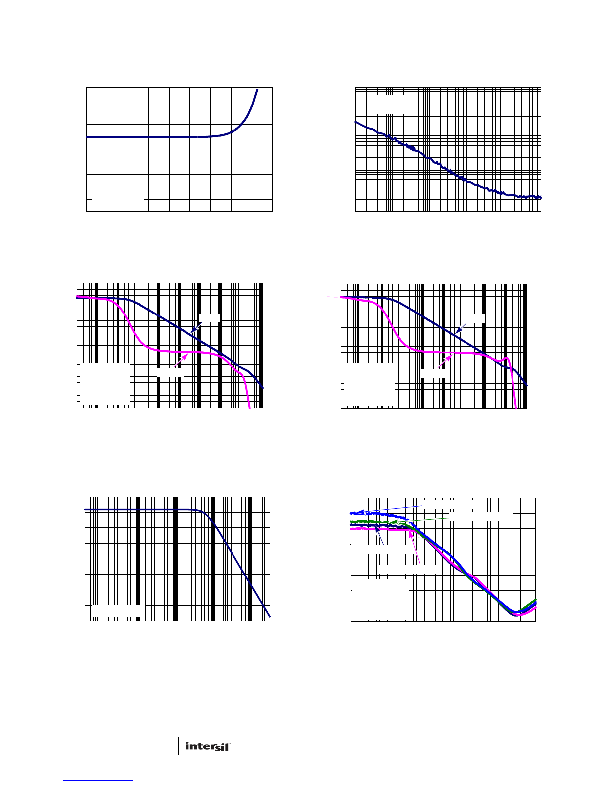
Typical Performance Curves V
50
40
30
20
10
(pA)
0
BIAS
-10
I
-20
-30
-40
SIMULATION
-50
-40 -20 0 20 40 60 80 100 120 140
TEMPERATURE (°C)
FIGURE 2. INPUT BIAS CURRENT vs TEMPERATURE
120
100
80
60
40
20
0
= ±0.9V
V
+
-20
RL = 100k
OPEN LOOP GAIN (dB)
-40
= 10pF
C
L
-60
SIMULATION
-80
0.1 1 10 100 1k 10k 100k 1M 10M 100M
PHASE
FREQUENCY (Hz)
FIGURE 4. OPEN-LOOP GAIN, PHASE vs FREQUENCY,
R
= 100kΩ, CL = 10pF, VS= ±0.9V
L
GAIN
= ±2.5V, VCM = 0V, RL = Open, unless otherwise specified.
S
10,000
V+ = ±2.5V
A
= 1
V
1000
100
INPUT NOISE VOLTAGE (nV/√Hz)
10
1 10 100 1k 10k 100k
FREQUENCY (Hz)
FIGURE 3. INPUT NOISE VOLTAGE SPECTRAL DENSITY
20
0
-20
-40
-60
-80
-100
-120
-140
-160
-180
PHASE (°)
120
100
80
60
40
20
0
V
= ±2.5V
+
-20
RL = 100k
OPEN LOOP GAIN (dB)
-40
C
= 10pF
L
-60
SIMULATION
-80
0.1 1 10 100 1k 10k 100k 1M 10M 100M
PHASE
FREQUENCY (Hz)
FIGURE 5. OPEN-LOOP GAIN, PHASE vs FREQUENCY,
R
=100kΩ, CL = 10pF, VS = ±2.5V
L
GAIN
20
0
-20
-40
-60
-80
-100
-120
-140
-160
-180
PHASE (°)
80
70
60
50
40
CMRR (dB)
30
20
10
SIMULATION
0
0.01 0.1 1 10 100 1k 10k 100k 1M 10M 100M
FREQUENCY (Hz)
FIGURE 6. CMRR vs FREQUENCY, V
6
= ±2.5
S
80
70
60
50
PSRR+ VS = ±0.9V
40
30
PSRR (dB )
20
10
0
100 1k 10k 100k 1M 10M
PSRR+ VS = ±2.5V
RL = INF
CL = 4pF
= +1
A
V
V
= 100mV
CM
FIGURE 7. PSRR vs FREQUENCY, V
PSRR- VS = ±2.5V
P-P
FREQUENCY (Hz)
PSRR- VS = ±0.9V
= ±0.9V, ±2.5V
S
FN6728.5
June 9, 2011
Page 7
ISL28113, ISL28213, ISL28413
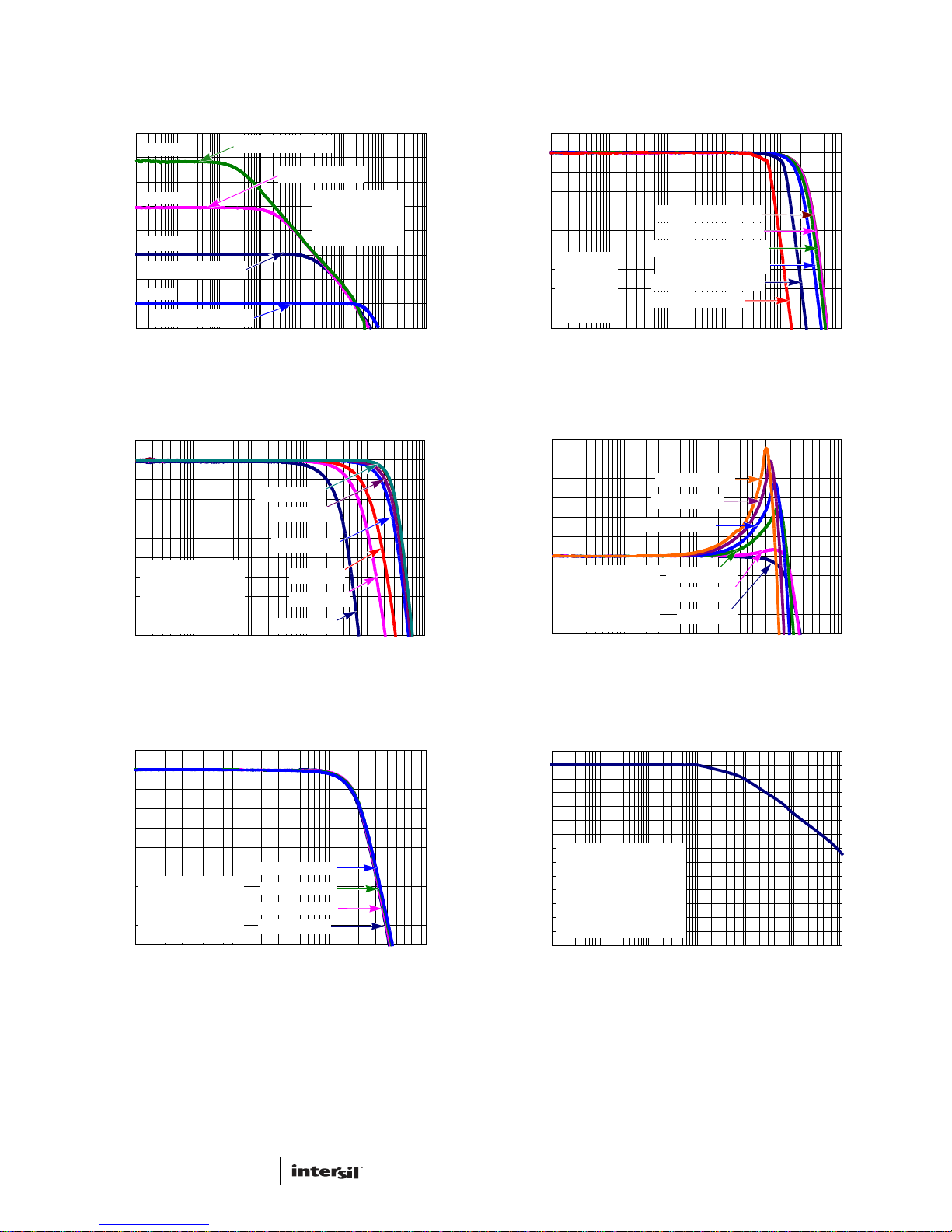
Typical Performance Curves V
70
A
= 1000
V
60
50
A
= 100
V
40
30
AV = 10
GAIN (dB)
20
Rg = 10k, Rf = 100k
10
AV = 1
0
Rg = OPEN, Rf = 0
-10
10
100
FIGURE 8. FREQUENCY RESPONSE vs CLOSED LOOP GAIN
1
0
-1
-2
-3
-4
-5
V+ = ±2.5V
-6
CL = 4pF
-7
NORMALIZED GAIN (dB)
= +1
A
V
-8
V
= 50mV
OUT
-9
100 1k 10k 100k 1M 10M
FIGURE 10. GAIN vs FREQUENCY vs R
Rg = 100, Rf = 100k
10k
1k
FREQUENCY (Hz)
RL = 49.9k
P-P
FREQUENCY (Hz)
Rg = 1k, Rf = 100k
V+ = ±2.5V
CL = 4pF
R
= 10k
L
V
= 50mV
OUT
100k 1M 10M
RL = 10k
RL = 4.99k
RL = 1k
RL = 499
RL = 100
P-P
L
= ±2.5V, VCM = 0V, RL = Open, unless otherwise specified. (Continued)
S
1
0
-1
-2
100M
-3
-4
-5
VS = ±2.5V
-6
C
= 4pF
L
-7
NORMALIZED GAIN (dB)
= +1
A
V
-8
R
= 10k
L
-9
100 1k 10k 100k 1M 10M
V
= 10mV
OUT
V
OUT
V
OUT
V
OUT
V
OUT
V
OUT
FREQUENCY (Hz)
= 50mV
= 100mV
= 200mV
= 500mV
= 1V
P-P
P-P
P-P
P-P
P-P
P-P
FIGURE 9. FREQUENCY RESPONSE vs V
6
5
-1
-2
NORMALIZED GAIN (dB)
-3
-4
4
3
2
1
0
VS = ±2.5V
R
L
A
V
V
OUT
1k
= 10k
= +1
= 50mV
CL = 474pF
CL = 224pF
P-P
10k
FREQUENCY (Hz)
CL = 1004pF
CL = 104pF
CL = 26pF
CL = 4pF
100k 1M 10M
FIGURE 11. GAIN vs FREQUENCY vs C
OUT
L
1
0
-1
-2
-3
-4
NORMALIZED GAIN (dB)
-5
-6
-7
-8
-9
10k
CL = 4pF
R
= 10k
L
A
= +1
V
V
= 50mV
OUT
P-P
VS = ±2.5V
VS = ±1.75V
VS = ±1.25V
VS = ±0.9V
100k 1M 10M
FREQUENCY (Hz)
FIGURE 12. GAIN vs FREQUENCY vs SUPPLY VOLTAGE
7
140
120
100
80
= ±2.5V
V
S
60
-DRIVER = INF
R
L
RL-RECEIVER = 10k
40
CROSS-TALK (dB)
CL = 4pF
= +1
A
V
20
V
0
10 100 1k 10k 100k 1M 10M
= 1V
SOURCE
P-P
FREQUENCY (Hz)
FIGURE 13. CROSSTALK, V
= ±2.5V
S
FN6728.5
June 9, 2011
Page 8

ISL28113, ISL28213, ISL28413
Typical Performance Curves V
30
20
10
0
-10
SMALL SIGNAL (mV)
-20
-30
0 200 400 600 800 1000 1200 1400 1600 1800 2000
FIGURE 14. SMALL SIGNAL TRANSIENT RESPONSE, VS= ±2.5V
0.1
0
-0.1
-0.2
-0.3
INPUT (V)
-0.4
VS = ±2.5V
RL = 10k
= 15pF
C
L
= +1
A
V
V
= 50mV
OUT
INPUT
OUTPUT @ VS = ±2.5V
P-P
TIME (ns)
RL = INF
C
= 15pF
L
=10
A
V
= 9.09k, Rg = 1k
R
f
OUTPUT @ VS=±0.9V
= ±2.5V, VCM = 0V, RL = Open, unless otherwise specified. (Continued)
S
3
2
1
0
-1
LARGE SIGNAL (V)
-2
-3
0 2 4 6 8 101214161820
VS = ±2.5V
VS = ±0.9V
RL = 10k
= 15pF
C
L
= +1
A
V
V
= RAIL
OUT
TIME (ms)
FIGURE 15. LARGE SIGNAL TRANSIENT RESPONSE vs R
V
= ±0.9V, ±2.5V
S
0.5
0
-0.5
-1.0
-1.5
-2.0
OUTPUT (V)
0.6
0.5
0.4
0.3
0.2
INPUT (V)
0.1
OUTPUT @ VS = ±2.5V
OUTPUT @ VS=±0.9V
RL = INF
= 15pF
C
L
=10
A
V
= 9.09k, Rg = 1k
R
f
L
3.0
2.5
2.0
1.5
1.0
OUTPUT (V)
0.5
-0.5
-0.6
012345678910
TIME (ms)
FIGURE 16. NEGATIVE OUTPUT OVERLOAD RESPONSE TIME,
V
= ±0.9V, ±2.5V
S
90
VS = ±2.5V
= 10k
R
80
L
A
= 1
V
70
60
50
40
30
OVERSHOOT (%)
20
10
= 50mV
V
OUT
0
10 100 1k 10k
FIGURE 18. % OVERSHOOT vs LOAD CAPACITANCE, V
-2.5
-3.0
P-P
T
O
O
H
S
R
E
V
O
H
S
R
E
V
O
CAPACITANCE (pF)
0
-0.1
012345678910
INPUT
TIME (ms)
FIGURE 17. POSITIVE OUTPUT OVERLOAD RESPONSE TIME,
V
= ±0.9V, ±2.5V
S
+
-
T
O
O
= ±2.5V
S
0
-0.5
8
FN6728.5
June 9, 2011
Page 9

ISL28113, ISL28213, ISL28413
Applications Information
Functional Description
The ISL28113, ISL28213 and ISL28413 are single, dual and
quad, CMOS rail-to-rail input, output (RRIO) micropower
operational amplifiers. They are designed to operate from single
supply (1.8V to 5.5V) or dual supply (±0.9V to ±2.75V). The parts
have an input common mode range that extends 100mV above
and below the power supply voltage rails. The output stage can
swing to within 15mV of the supply rails with a 10kΩ load.
Input ESD Diode Protection
All input terminals have internal ESD protection diodes to both
positive and negative supply rails, limiting the input voltage to
within one diode beyond the supply rails (see “Pin Descriptions Circuit 1” on page 3
may exceed either power supply voltage by 0.5V or more, an
external series resistor must be used to ensure the input currents
never exceed 20mA (see Figure 19).
VIN-
). For applications where the input voltage
R
F
V+
RIN-
-
RIN+
+
R
G
V-
R
L
Power Dissipation
It is possible to exceed the +125°C maximum junction
temperatures under certain load, power supply conditions and
ambient temperature conditions. It is therefore important to
calculate the maximum junction temperature (T
applications to determine if power supply voltages, load
conditions, or package type need to be modified to remain in the
safe operating area. These parameters are related using
Equation 1:
T
JMAXTMAXθJA
xPD
+=
MAXTOTAL
where:
•P
DMAXTOTAL
each amplifier in the package (PD
•PD
MAX
PD
MAXVSIqMAXVS
is the sum of the maximum power dissipation of
)
MAX
for each amplifier can be calculated using Equation 2:
V
OUTMAX
( - V
OUTMAX
------------------------
)
×+×=
R
L
where:
= Maximum ambient temperature
•T
MAX
• θJA = Thermal resistance of the package
•PD
= Maximum power dissipation of 1 amplifier
MAX
•VS = Total supply voltage
•I
•V
= Maximum quiescent supply current of 1 amplifier
qMAX
OUTMAX
= Maximum output voltage swing of the application
•RL = Load resistance
JMAX
) for all
(EQ. 1)
(EQ. 2)
FIGURE 19. INPUT ESD DIODE CURRENT LIMITING
Output Phase Reversal
Output phase reversal is a change of polarity in the amplifier
transfer function when the input voltage exceeds the supply
voltage. The ISL28113, ISL28213 and ISL28413 are immune to
output phase reversal, even when the input voltage is 1V beyond
the supplies.
Unused Channels
If the application requires less than all amplifiers one channel,
the user must configure the unused channel(s) to prevent it from
oscillating. The unused channel(s) will oscillate if the input and
output pins are floating. This will result in higher than expected
supply currents and possible noise injection into the channel
being used. The proper way to prevent this oscillation is to short
the output to the inverting input and ground the positive input (as
shown in Figure 20).
-
+
FIGURE 20. PREVENTING OSCILLATIONS IN UNUSED CHANNELS
ISL28113, ISL28213 and ISL28413 SPICE
Model
Figure 21 shows the SPICE model schematic and Figure 22 shows
the net list for the SPICE model. The model is a simplified version
of the actual device and simulates important AC and DC
parameters. AC parameters incorporated into the model are: 1/f
and flatband noise, Slew Rate,
parameters are IOS, total supply current and output voltage swing.
The model uses typical parameters given in the “Electrical
Specifications” Table beginning on page 4. The AVOL is adjusted
for 85dB with the dominate pole at 100Hz. The CMRR is set 72dB,
f = 35kHz). The input stage models the actual device to present an
accurate AC representation. The model is configured for ambient
temperature of +25°C.
Figures 23 through 32 show the characterization vs simulation
results for the Noise Voltage, Closed Loop Gain vs Frequency,
Large Signal 5V Step Response, CMRR and Open Loop Gain
Phase.
CMRR, Gain and Phase. The DC
9
FN6728.5
June 9, 2011
Page 10

ISL28113, ISL28213, ISL28413
LICENSE STATEMENT
The information in this SPICE model is protected under the
United States copyright laws. Intersil Corporation hereby grants
users of this macro-model hereto referred to as “Licensee”, a
nonexclusive, nontransferable licence to use this model as long
as the Licensee abides by the terms of this agreement. Before
using this macro-model, the Licensee should read this license. If
the Licensee does not accept these terms, permission to use the
model is not granted.
The Licensee may not sell, loan, rent, or license the
macro-model, in whole, in part, or in modified form, to anyone
outside the Licensee’s company. The Licensee may modify the
macro-model to suit his/her specific applications, and the
Licensee may make copies of this macro-model for use within
their company only.
This macro-model is provided “AS IS, WHERE IS, AND WITH NO
WARRANTY OF ANY KIND EITHER EXPRESSED OR IMPLIED,
INCLUDING BUY NOT LIMITED TO ANY IMPLIED WARRANTIES OF
MERCHANTABILITY AND FITNESS FOR A PARTICULAR PURPOSE.”
In no event will Intersil be liable for special, collateral, incidental,
or consequential damages in connection with or arising out of
the use of this macro-model. Intersil reserves the right to make
changes to the product and the macro-model without prior
notice.
10
FN6728.5
June 9, 2011
Page 11

ISL28113, ISL28213, ISL28413
En
V++
4
5
Vc
Vmid
V--
VCM
V+
Vg
Vmid
V-
V--
Vin+
En
Vin-
V--
V++
R21
800E3
V9
-
+
0.00035V
R22
5E11
+
CinDiff
1.02pF
Cin1
1.26pF
G1
17
R23
5E11
-
G2
+
18
1ST Gain Stage (Cont)
+
+
-
-
-
+
29
90uA
-
+
+
+
-
-
Voltage Noise Stage
28
DN
D13
Vc
+
+
Vmid
-
-
In+
1
M14
R11
1
R12
1
Cin2
1.26pF
D3
DX
+
V3
0.61V
-
16
+
0.61V
-
D4
DX
E2
ISY
E3
EOS
V4
V+
V-
2
R1
1.0004
3
R3
10
5
Input Stage
G7
+
-
-
+
G8
+
V1
1E-6V
-
R2
1.0004
4
R4
10
7
5E-3
G3
+
6
M15
I1
19
-
G4
-
+
20
2nd Gain Stage
C4
10pF
R17
5305.32
23
R18
5305.32
C3
10pF
M16
IOS
25E-12
D5
DX
+
V5
-
0.604V
Vg
0.604V
+
V6
-
D6
DX
D11
DY
D7
D8
9
11
R7
R13
5.0nF
5.0nF
R14
8
R5
10
1
13
+
-
318.329E3
C2
C3
318.329E3
DX
24
DX
25
+
-
G9
I2
5E-3
10
M17
R6
10
12
R8
1
1E-6V
V2
Vmid
E4
+
+
-
-
Mid Supply Ref
D9
DX
26
27
+
-
G10
+
-
G1A
G2A
+
D10
DX
+
-
RA1
1
14
RA2
1
R9
100
DX
DX
1ST Gain Stage
G5
+
-
G6
-
21
Vc
22
+
VCM
Common Mode Gain Stage
G11
-
V7
V8
-
0.08V
+
+
VOUT
0.08V
G12
-
D12
DY
+
D1
D2
L1
4.5474
R15
1E6
R16
1E6
L2
4.5474
R19
50
R20
50
V++
R10
1E9
4
15
5
Vc
Vmid
V--
VCM
V++
Vg
Vmid
V--
V
OUT
Supply Isolation Stage
Pole Stage
11
FIGURE 21. SPICE SCHEMATICFIGURE 21. SPICE SCHEMATIC
Output Stage
FN6728.5
June 9, 2011
Page 12

ISL28113, ISL28213, ISL28413
* source ISL28113_SPICEmodel
* Revision D, LaFontaine February 22, 2010 Improved noise
performance
* Model for Noise, supply currents, CMRR 72dB f=35kHz, AVOL
85dB f=100Hz
* SR = 1.0V/us, GBWP 2MHz, 2nd pole 3MHz Output voltage clamp
and short ckt I limit
*Copyright 2009 by Intersil Corporation
*Refer to data sheet “LICENSE STATEMENT” Use of
*this model indicates your acceptance with the
*terms and provisions in the License Statement.
* Connections: +input
* | -input
* | | +Vsupply
* | | | -Vsupply
* | | | | output
* | | | | |
.subckt ISL28113subckt Vin+ Vin- V+ V- VOUT
* source ISL28113_DS rev1
*
*Voltage Noise
E_En VIN+ EN 28 0 1
D_D13 29 28 DN
V_V9 29 0 0.45
R_R21 28 0 30
*
*Input Stage
M_M14 3 1 5 5 NCHANNELMOSFET
M_M15 4 VIN- 6 6 NCHANNELMOSFET
M_M16 11 VIN- 9 9 PMOSISIL
M_M17 12 1 10 10 PMOSISIL
I_I1 7 V-- DC 5e-3
I_I2 V++ 8 DC 5e-3
I_IOS VIN- 1 DC 25e-12
G_G1A V++ 14 4 3 1404
G_G2A V-- 14 11 12 1404
V_V1 V++ 2 1e-6
V_V2 13 V-- 1e-6
R_R1 3 2 1.0004
R_R2 4 2 1.0004
R_R3 5 7 10
R_R4 7 6 10
R_R5 9 8 10
R_R6 8 10 10
R_R7 13 11 1
R_R8 13 12 1
R_RA1 14 V++ 1
R_RA2 V-- 14 1
C_CinDif VIN- EN 1.02E-12
C_Cin1 V-- EN 1.26e-12
C_Cin2 V-- VIN- 1.26e-12
*
*1st Gain Stage
G_G1 V++ 16 15 VMID 334.753e-3
G_G2 V-- 16 15 VMID 334.753e-3
V_V3 17 16 .61
V_V4 16 18 .61
D_D1 15 VMID DX
D_D2 VMID 15 DX
D_D3 17 V++ DX
D_D4 V-- 18 DX
R_R9 15 14 100
R_R10 15 VMID 1e9
R_R11 16 V++ 1
R_R12 V-- 16 1
*
*2nd Gain Stage
G_G3 V++ VG 16 VMID 24.893e-3
G_G4 V-- VG 16 VMID 24.893e-3
V_V5 19 VG .604
V_V6 VG 20 .604
D_D5 19 V++ DX
D_D6 V-- 20 DX
R_R13 VG V++ 318.329e3
R_R14 V-- VG 318.329e3
C_C2 VG V++ 5E-09
C_C3 V-- VG 5E-09
*
*Mid supply Ref
E_E4 VMID V-- V++ V-- 0.5
E_E2 V++ 0 V+ 0 1
E_E3 V-- 0 V- 0 1
I_ISY V+ V- DC 90e-6
*
*Common Mode Gain Stage with Zero
G_G5 V++ VC VCM VMID 0.25118
G_G6 V-- VC VCM VMID 0.25118
E_EOS 1 EN VC VMID 1
R_R15 VC 21 0.001
R_R16 22 VC 0.001
R_R22 EN VCM 5e11
R_R23 VCM VIN- 5e11
L_L1 21 V++ 4.547418E-09
L_L2 22 V-- 4.547418E-09
*
*Pole Stage
G_G7 V++ 23 VG VMID 0.18849
G_G8 V-- 23 VG VMID 0.18849
R_R17 23 V++ 5.30532
R_R18 V-- 23 5.30532
C_C4 23 V++ 1e-8
C_C5 V-- 23 1e-8
*
*Output Stage with Correction Current Sources
G_G9 26 V-- VOUT 23 0.02
G_G10 27 V-- 23 VOUT 0.02
G_G11 VOUT V++ V++ 23 0.02
G_G12 V-- VOUT 23 V-- 0.02
V_V7 24 VOUT .08
V_V8 VOUT 25 .08
D_D7 23 24 DX
D_D8 25 23 DX
D_D9 V++ 26 DX
D_D10 V++ 27 DX
D_D11 V-- 26 DY
D_D12 V-- 27 DY
R_R19 VOUT V++ 50
R_R20 V-- VOUT 50
.model pmosisil pmos (kp=16e-3 vto=-0.6)
.model NCHANNELMOSFET nmos (kp=3e-3 vto=0.6)
.model DN D(KF=6.69e-9 AF=1)
.MODEL DX D(IS=1E-12 Rs=0.1)
.MODEL DY D(IS=1E-15 BV=50 Rs=1)
.ends ISL28113subckt
12
FIGURE 22. SPICE NET LIST
FN6728.5
June 9, 2011
Page 13

ISL28113, ISL28213, ISL28413
Characterization vs Simulation Results
10,000
V+ = ±2.5V
= 1
A
V
10,000
1000
100
INPUT NOISE VOLTAGE (nV/√Hz)
10
1 10 100 1k 10k 100k
FREQUENCY (Hz)
FIGURE 23. CHARACTERIZED INPUT NOISE VOLTAGE
70
A
= 1000
V
60
50
= 100
A
V
40
30
AV = 10
GAIN (dB)
20
Rg = 10k, Rf = 100k
10
AV = 1
0
-10
10
Rg = OPEN, Rf = 0
100
Rg = 100, Rf = 100k
Rg = 1k, Rf = 100k
10k
1k
FREQUENCY (Hz)
V+ = ±2.5V
CL = 4pF
= 10k
R
L
= 50mV
V
OUT
100k 1M 10M
P-P
100M
FIGURE 25. CHARACTERIZED CLOSED LOOP GAIN vs FREQUENCY
1000
100
INPUT NOISE VOLTAGE (nV/√Hz)
10
1 10 100 1k 10k 100k
FREQUENCY (Hz)
FIGURE 24. SIMULATED INPUT NOISE VOLTAGE
70
60
40
20
GAIN (dB)
0
-10
10 100 1.0k 10k 100k 1.0M 10M 100M
(A) AC sims.dat (active)
FREQUENCY (Hz)
FIGURE 26. SIMULATED CLOSED LOOP GAIN vs FREQUENCY
3
2
1
0
-1
LARGE SIGNAL (V)
-2
-3
02468101214161820
VS = ±2.5V
VS = ±0.9V
RL = 10k
C
= 15pF
L
A
= +1
V
= RAIL
V
OUT
TIME (ms)
FIGURE 27. CHARACTERIZED LARGE SIGNAL TRANSIENT
RESPONSE vs R
, VS= ±0.9V, ±2.5V
L
13
3
2
1
-0
-1
LARGE SIGNAL (V)
-2
-3
051015202530
(A) AC sims.dat (active)
V
OUT
V
IN
RL = 10k
C
= 15pF
L
A
= +10
V
V
= RAIL
OUT
TIME (µs)
VS = ±2.5V
FIGURE 28. SIMULATED LARGE SIGNAL TRANSIENT RESPONSE vs
R
, VS = ±0.9V, ±2.5V
L
FN6728.5
June 9, 2011
Page 14

ISL28113, ISL28213, ISL28413
Characterization vs Simulation Results (Continued)
120
100
80
60
40
20
0
= ±2.5V
V
+
-20
RL = 100k
OPEN LOOP GAIN (dB)
-40
C
= 10pF
L
-60
SIMULATION
-80
0.1 1 10 100 1k 10k 100k 1M 10M 100M
PHASE
FREQUENCY (Hz)
GAIN
20
0
-20
-40
-60
-80
-100
-120
-140
-160
-180
FIGURE 29. SIMULATED (DESIGN) OPEN-LOOP GAIN, PHASE vs
FREQUENCY
80
70
60
50
40
30
CMRR (dB)
20
10
SIMULATION
0
0.01 0.1 1 10 100 1k 10k 100k 1M 10M 100M
FREQUENCY (Hz)
FIGURE 31. SIMULATED (DESIGN) CMRR
200
160
120
80
PHASE (°)
40
0
OPEN LOOP GAIN (dB)/PHASE (°)
0.01 0.1 10 100 1.0k 10k 100k 1.0M 10M 100M
(A) AC sims.dat (active)
1.0
FREQUENCY (Hz)
FIGURE 30. SIMULATED (SPICE) OPEN-LOOP GAIN, PHASE vs
FREQUENCY
80
60
)
40
CMRR (dB
20
0
0.01 0.1 1.0 1.0k 10k 100k 10M
(A) AC sims.dat (active)
100 1.0M 100M10
FREQUENCY (Hz)
FIGURE 32. SIMULATED (SPICE) CMRR
14
FN6728.5
June 9, 2011
Page 15

ISL28113, ISL28213, ISL28413
Revision History
The revision history provided is for informational purposes only and is believed to be accurate, but not warranted. Please go to Web to make sure you
have the latest Rev.
DATE REVISION CHANGE
5/18/11 FN6728.5 - On page 2, Ordering Information table: ISL28113FHZ-T7 & -T7A PKG DWG # changed from MDP0038 (Obsoleted) to
P5.064A. Removed ISL28213FHZ and added “Coming Soon” to parts ISL28213FHZ-T7A and ISL28413TSSOPEVAL1Z.
- On page 3, Pin Descriptions: Circuit 3 diagram, removed anti-parallel diodes from the IN+ to IN- terminals.
- On page 4, Absolute Maximum Ratings: changed Differential Input Voltage from "0.5V" to "V
- On page 4, updated CMRR and PSRR parameters in Electrical Specifications table with test condition specifiying -40°C
to 125°C typical parameter.
- On page 5, updated Note 6 (“over-temp” note) referenced in MIN and MAX column headings of Electrical Specifications
table from "Parameters with MIN and/or MAX limits are 100% tested at +25°C, unless otherwise specified. Temperature
limits established by characterization and are not production tested." to new standard "Compliance to datasheet limits is
assured by one or more methods: production test, characterization and/or design."
- On page 9, under “Input ESD Diode Protection,” removed “They also contain back to-back diodes across the input
terminals.” Changed “For applications where the input differential voltage is expected to exceed 0.5V, an external series
resistor...” to “For applications where the input differential voltage may exceed either power supply voltage by 0.5V or
more, an external series resistor...”. Removed “Although the amplifier is fully protected, high input slew rates that exceed
the amplifier slew rate (±1V/µs) may cause output distortion.”
- On page 9, Figure 19: updated circuit schematic by removing back-to-back input protection diodes.
- On page 18, replaced Package Outline Drawing MDP0038 (obsolete) with P5.064A.
3/23/10 FN6728.4 Page 1, 2nd paragraph - Added “...SOT23-8 packages...” and changed “SO8” to “SOIC8”.
Also global, changed S08 to SOIC8
Pg 2, Ordering Information table: Part # ISL28213FEZ changed to ISL28213FHZ and Part Marking changed to "TBD"
-Added Related Literature on page 1, updated ordering information by adding Eval boards.
-Added to ordering information part number ISL28213FHZ 8 Ld SOT-23 Package as coming soon.
-Replaced Figure 24 Simulated Input Noise Voltage with following changes:
Y-axis from “10 to 100” to “10,000 to 10”
Removed (A) AC sims.dat (active) from top of graph
Curve changed to improve noise performance
Made changes to Spice Net List as follows:
-Changed Revision from “C” to “D” and added improved noise performance to Revision line.
-Changed in Voltage Noise
“V_V9 29 0 .00035” to “V_V9 29 0 0.45”
“R_R21 28 0 800E3 TC=0,0” to “R_R21 28 0 30”
-Removed TC=0 in Input Stage from R_R1 through C_Cin2
-Removed TC=0 in 1st Gain Stage from R_R9 through R_R12
-Removed TC=0 in 2nd Gain Stage from R_R13 through C_C3
-Changed in Common Mode Gain Stage with Zero
“G_G5 V++ VC VCM VMID 2.5118E-10” to “G_G5 V++ VC VCM VMID 0.25118”
“G_G6 V-- VC VCM VMID 2.5118E-10” to “G_G6 V-- VC VCM VMID 0.25118”
Removed TC=0 from R_R16 through R_R23
-Changed in Pole Stage
“G_G7 V++ 23 VG VMID 188.49e-6” to ‘G_G7 V++ 23 VG VMID 0.18849”
“G_G8 V-- 23 VG VMID 188.49e-6” to “G_G8 V-- 23 VG VMID 0.18849”
Removed TC=0 from R_R17 through C_C5
Removed TC=0 in Output Stage with Correction Current Sources from R_R19 and R_R20
Made changes to Spice Schematic Figure 21 as follows:
-Input Stage - Modified connection to the EOS (voltage control voltage source)
-Added to Thermal Information 8 LD SOT-23 as TBD
-Added to pin configuration for the ISL28213 8 Ld SOT-23
12/16/09 FN6728.3 Removed “Coming Soon” from MSOP package options in the “Ordering Information” on page 2.
Updated the Theta JA for the MSOP package option from 170°C/W to 180°C/W on page 4.
11/17/09 FN6728.2 Removed “Coming Soon” from SC70 and SOT-23 package options in the “Ordering Information” on page 2.
11/12/09 FN6728.1 Changed theta Ja to 250 from 300.
10/26/09 FN6728.0 Initial Release
Added license statement (page 10) and reference in spice model (page 12).
- 0.5V to V+ + 0.5V".
-
15
FN6728.5
June 9, 2011
Page 16

ISL28113, ISL28213, ISL28413
Products
Intersil Corporation is a leader in the design and manufacture of high-performance analog semiconductors. The Company's products
address some of the industry's fastest growing markets, such as, flat panel displays, cell phones, handheld products, and notebooks.
Intersil's product families address power management and analog signal processing functions. Go to www.intersil.com/products for a
complete list of Intersil product families.
*For a complete listing of Applications, Related Documentation and Related Parts, please see the respective device information page
on intersil.com: ISL28113
To report errors or suggestions for this datasheet, please go to www.intersil.com/askourstaff
FITs are available from our website at http://rel.intersil.com/reports/search.php
, ISL28213, ISL28413
For additional products, see www.intersil.com/product_tree
Intersil products are manufactured, assembled and tested utilizing ISO9000 quality systems as noted
in the quality certifications found at www.intersil.com/design/quality
Intersil products are sold by description only. Intersil Corporation reserves the right to make changes in circuit design, software and/or specifications at any time
without notice. Accordingly, the reader is cautioned to verify that data sheets are current before placing orders. Information furnished by Intersil is believed to be
accurate and reliable. However, no responsibility is assumed by Intersil or its subsidiaries for its use; nor for any infringements of patents or other rights of third
parties which may result from its use. No license is granted by implication or otherwise under any patent or patent rights of Intersil or its subsidiaries.
For information regarding Intersil Corporation and its products, see www.intersil.com
16
FN6728.5
June 9, 2011
Page 17

ISL28113, ISL28213, ISL28413
Small Outline Transistor Plastic Packages (SC70-5)
E
A2
A
SEATING
PLANE
D
e1
123
e
C
L
0.20 (0.008) M
PLATING
4X θ1
C
4X θ1
C
L
WITH
C
c
BASE METAL
45
C
b
A1
0.10 (0.004) C
b
b1
R1
L
α
L1
L
R
VIEW C
C
L
SEATING
PLANE
-C-
c1
GAUGE PLANE
L2
E1
P5.049
5 LEAD SMALL OUTLINE TRANSISTOR PLASTIC PACKAGE
INCHES MILLIMETERS
SYMBOL
A 0.031 0.043 0.80 1.10 A1 0.000 0.004 0.00 0.10 A2 0.031 0.039 0.80 1.00 -
b 0.006 0.012 0.15 0.30 -
b1 0.006 0.010 0.15 0.25
c 0.003 0.009 0.08 0.22 6
c1 0.003 0.009 0.08 0.20 6
C
D 0.073 0.085 1.85 2.15 3
E 0.071 0.094 1.80 2.40 E1 0.045 0.053 1.15 1.35 3
e 0.0256 Ref 0.65 Ref -
e1 0.0512 Ref 1.30 Ref -
L 0.010 0.018 0.26 0.46 4
L1 0.017 Ref. 0.420 Ref. L2 0.006 BSC 0.15 BSC
o
α
0
o
8
o
0
N5 55
R 0.004 - 0.10 -
R1 0.004 0.010 0.15 0.25
NOTES:
1. Dimensioning and tolerances per ASME Y14.5M-1994.
2. Package conforms to EIAJ SC70 and JEDEC MO-203AA.
3. Dimensions D and E1 are exclusive of mold flash, protrusions,
or gate burrs.
4. Footlength L measured at reference to gauge plane.
5. “N” is the number of terminal positions.
6. These Dimensions apply to the flat section of the lead between
0.08mm and 0.15mm from the lead tip.
7. Controlling dimension: MILLIMETER. Converted inch dimensions are for reference only.
o
8
NOTESMIN MAX MIN MAX
-
Rev. 3 7/07
VIEW C
0.4mm
0.75mm
2.1mm
0.65mm
TYPICAL RECOMMENDED LAND PATTERN
17
FN6728.5
June 9, 2011
Page 18

ISL28113, ISL28213, ISL28413
Package Outline Drawing
P5.064A
5 LEAD SMALL OUTLINE TRANSISTOR PLASTIC PACKAGE
Rev 0, 2/10
1.90
D
A
PIN 1
INDEX AREA
0.15 C2xD
B
5
2
TOP VIEW
4
0.95
0.40 ±0.05
0.20 C A-B DM
2.80
3
3
0.20 C
2x
1.60
0-3°
0.08-0.20
5
3
(0.60)
SEE DETAIL X
END VIEW
(2.40)
2.90
SIDE VIEW
(0.95)
10° TYP
(2 PLCS)
5
0.15 C2xA-B
1.14 ±0.15
0.05-0.15
(0.60)
(1.20)
1.45 MAX
C
0.10 C
NOTES:
Dimensions are in millimeters.1.
Dimensions in ( ) for Reference Only.
Dimensioning and tolerancing conform to ASME Y14.5M-1994.
2.
3.
Dimension is exclusive of mold flash, protrusions or gate burrs.
Foot length is measured at reference to guage plane.
4.
This dimension is measured at Datum “H”.
5.
Package conforms to JEDEC MO-178AA.
6.
SEATING PLANE
DETAIL "X"
H
(0.25)
0.45±0.1
GAUGE
PLANE
4
(1.90)
TYPICAL RECOMMENDED LAND PATTERN
18
FN6728.5
June 9, 2011
Page 19

ISL28113, ISL28213, ISL28413
Package Outline Drawing
M8.118A
8 LEAD MINI SMALL OUTLINE PLASTIC PACKAGE (MSOP)
Rev 0, 9/09
3.0±0.1
A
PIN# 1 ID
H
0.33 +0.07/ -0.08
0.08 C A B
8
1
2
TOP VIEW
SIDE VIEW 1
0.25 C AB
3.0±0.1
B
0.65 BSC
0.10 ± 0.05
4.9±0.15
0.86±0.09
SEATING PLANE
0.10 C
DETAIL "X"
1.10 Max
GAUGE
PLANE
0.18 ± 0.05
0.25
3°±3°
SIDE VIEW 2
0.95 BSC
C
0.55 ± 0.15
DETAIL "X"
5.80
4.40
3.00
0.65
TYPICAL RECOMMENDED LAND PATTERN
19
1.40
0.40
NOTES:
Dimensions are in millimeters.1.
Dimensioning and tolerancing conform to JEDEC MO-187-AA
2.
and AMSE Y14.5m-1994.
3.
Plastic or metal protrusions of 0.15mm max per side are not
included.
Plastic interlead protrusions of 0.25mm max per side are not
4.
included.
Dimensions “D” and “E1” are measured at Datum Plane “H”.
5.
This replaces existing drawing # MDP0043 MSOP 8L.
6.
FN6728.5
June 9, 2011
Page 20

ISL28113, ISL28213, ISL28413
Package Outline Drawing
M8.15E
8 LEAD NARROW BODY SMALL OUTLINE PLASTIC PACKAGE
Rev 0, 08/09
PIN NO.1
ID MARK
5
1.75 MAX
1.27
4.90 ± 0.10
TOP VIEW
0.175 ± 0.075
SIDE VIEW “A
4
A
B
3.90 ± 0.10
4
0.43 ± 0.076
0.25 AMC B
6.0 ± 0.20
1.45 ± 0.1
DETAIL "A"
(0.35) x 45°
SIDE VIEW “B”
0.22 ± 0.03
4° ± 4°
0.25
GAUGE PLANE
SEATING PLANE
0.10 C
C
(1.27)
(5.40)
TYPICAL RECOMMENDED LAND PATTERN
20
(0.60)
(1.50)
0.63 ±0.23
DETAIL "A"
NOTES:
Dimensions are in millimeters.1.
Dimensions in ( ) for Reference Only.
Dimensioning and tolerancing conform to AMSE Y14.5m-1994.
2.
3.
Unless otherwise specified, tolerance : Decimal ± 0.05
Dimension does not include interlead flash or protrusions.
4.
Interlead flash or protrusions shall not exceed 0.25mm per side.
The pin #1 identifier may be either a mold or mark feature.
5.
Reference to JEDEC MS-012.
6.
FN6728.5
June 9, 2011
Page 21

ISL28113, ISL28213, ISL28413
Small Outline Package Family (SO)
A
D
NN
(N/2)+1
h X 45°
PIN #1
E
C
SEATING
PLANE
0.004 C
E1
B
0.010 BM CA
I.D. MARK
1
e
0.010 BM CA
(N/2)
c
SEE DETAIL “X”
L1
H
A2
GAUGE
PLANE
A1
b
DETAIL X
L
4° ±4°
MDP0027
SMALL OUTLINE PACKAGE FAMILY (SO)
INCHES
SO16
SYMBOL
(0.150”)
A 0.068 0.068 0.068 0.104 0.104 0.104 0.104 MAX A1 0.006 0.006 0.006 0.007 0.007 0.007 0.007 ±0.003 A2 0.057 0.057 0.057 0.092 0.092 0.092 0.092 ±0.002 -
b 0.017 0.017 0.017 0.017 0.017 0.017 0.017 ±0.003 -
c 0.009 0.009 0.009 0.011 0.011 0.011 0.011 ±0.001 D 0.193 0.341 0.390 0.406 0.504 0.606 0.704 ±0.004 1, 3
E 0.236 0.236 0.236 0.406 0.406 0.406 0.406 ±0.008 -
E1 0.154 0.154 0.154 0.295 0.295 0.295 0.295 ±0.004 2, 3
e 0.050 0.050 0.050 0.050 0.050 0.050 0.050 Basic L 0.025 0.025 0.025 0.030 0.030 0.030 0.030 ±0.009 -
L1 0.041 0.041 0.041 0.056 0.056 0.056 0.056 Basic -
h 0.013 0.013 0.013 0.020 0.020 0.020 0.020 Reference N 8 14 16 16 20 24 28 Reference -
NOTES:
1. Plastic or metal protrusions of 0.006” maximum per side are not included.
2. Plastic interlead protrusions of 0.010” maximum per side are not included.
3. Dimensions “D” and “E1” are measured at Datum Plane “H”.
4. Dimensioning and tolerancing per ASME Y14.5M-1994
SO16 (0.300”)
(SOL-16)
SO20
(SOL-20)
SO24
(SOL-24)
SO28
(SOL-28)
TOLERANCE NOTESSO-8 SO-14
A
0.010
Rev. M 2/07
21
FN6728.5
June 9, 2011
Page 22

ISL28113, ISL28213, ISL28413
Thin Shrink Small Outline Package Family (TSSOP)
C
SEATING
PLANE
N LEADS
0.25 CAB
M
E
E1
B
0.10 C
N
1
TOP VIEW
e
b
SEE DETAIL “X”
(N/2)+1
SIDE VIEW
(N/2)
0.10 CABM
AD
PIN #1 I.D.
0.20 C2XB A
N/2 LEAD TIPS
0.05
MDP0044
THIN SHRINK SMALL OUTLINE PACKAGE FAMILY
MILLIMETERS
SYMBOL
A 1.20 1.20 1.20 1.20 1.20 Max
A1 0.10 0.10 0.10 0.10 0.10 ±0.05
A2 0.90 0.90 0.90 0.90 0.90 ±0.05
b 0.25 0.25 0.25 0.25 0.25 +0.05/-0.06
c 0.15 0.15 0.15 0.15 0.15 +0.05/-0.06
D 5.00 5.00 6.50 7.80 9.70 ±0.10
E 6.40 6.40 6.40 6.40 6.40 Basic
E1 4.40 4.40 4.40 4.40 4.40 ±0.10
H
e 0.65 0.65 0.65 0.65 0.65 Basic
L 0.60 0.60 0.60 0.60 0.60 ±0.15
L1 1.00 1.00 1.00 1.00 1.00 Reference
NOTES:
1. Dimension “D” does not include mold flash, protrusions or gate
burrs. Mold flash, protrusions or gate burrs shall not exceed
0.15mm per side.
2. Dimension “E1” does not include interlead flash or protrusions.
Interlead flash and protrusions shall not exceed 0.25mm per
side.
3. Dimensions “D” and “E1” are measured at dAtum Plane H.
4. Dimensioning and tolerancing per ASME Y14.5M-1994.
TOLERANCE14 LD 16 LD 20 LD 24 LD 28 LD
Rev. F 2/07
c
A2
A
A1
END VIEW
DETAIL X
L1
GAUGE
PLANE
0.25
L
0° - 8°
22
FN6728.5
June 9, 2011
 Loading...