

®
ISL24010
Octal Voltage Level Shifter for TFT/LCD Panels
Data Sheet November 4, 2005
High Voltage TFT-LCD Logic Driver
The ISL24010 is a high voltage TFT-LCD logic driver with a
+40V and -20V (momentary absolute max) output voltage
swing capability. It is manufactured using the Intersil’s
proprietary monolithic high voltage bipolar process and is
capable of driving a 3000pF load in 500ns.
The ISL24010 will level shift a digital input signal to an output
voltage nearly equal to its output supply voltages. The
ISL24010 has 3 supplies. V
ON1
and V
are positive
ON2
supplies with a voltage range between +10V and +40V
(absolute max). V
is the negative supply with a voltage
OFF
range between -5V and -20V (absolute max). Outputs 1
through 6 are connected to V
are connected to V
ON2
and V
and V
ON1
OFF
OFF
. This configuration
. Outputs 7 and 8
enables outputs 1 through 6 to provide slicing to the row
drivers to reduce flicker, and outputs 7 and 8 to control
possible supply lines. V
possible to tie V
ON1
should remain constant. It is
ON2
and V
supplies together, if
ON2
independent control as described above is not desired.
V
is required to be greater than or equal to V
ON2
ON1
at all
times.
The ISL24010 is available in TSSOP-20 pin package. It is
specified for operation over the -40°C to +85°C industrial
temperature range.
Ordering Information
TEMP.
PART
NUMBER
ISL24010IVZ
(See Note)
ISL24010IVZ-T
(See Note)
NOTE: Intersil Pb-free plus anneal products employ special Pb-free
material sets; molding compounds/die attach materials and 100%
matte tin plate termination finish, which are RoHS compliant and
compatible with both SnPb and Pb-free soldering operations. Intersil
Pb-free products are MSL classified at Pb-free peak reflow
temperatures that meet or exceed the Pb-free requirements of
IPC/JEDEC J STD-020.
PART
MARKING
24010IVZ -40 to +85 20 Ld TSSOP
24010IVZ -40 to +85 20 Ld TSSOP
RANGE
(°C) PACKAGE
(Pb-free)
Tape and Reel
(Pb-free)
PKG.
DWG. #
M20.173
M20.173
FN6124.0
Features
• 0V to 5.5V (absolute max) Input Voltage Range
• +40V and -20V (momentary absolute max) Output Voltage
Range
• 10mA Output Continuous Current (all 8 channels)
• 25mA Output Peak Current (all 8 channels)
• Rise/Fall Times 150ns/210ns
• Propagation Delay 250ns
• 50kHz Input Logic Frequency
• 20 Ld TSSOP Pb-Free Plus Anneal (RoHS Compliant)
Applications
• TFT-LCD panels
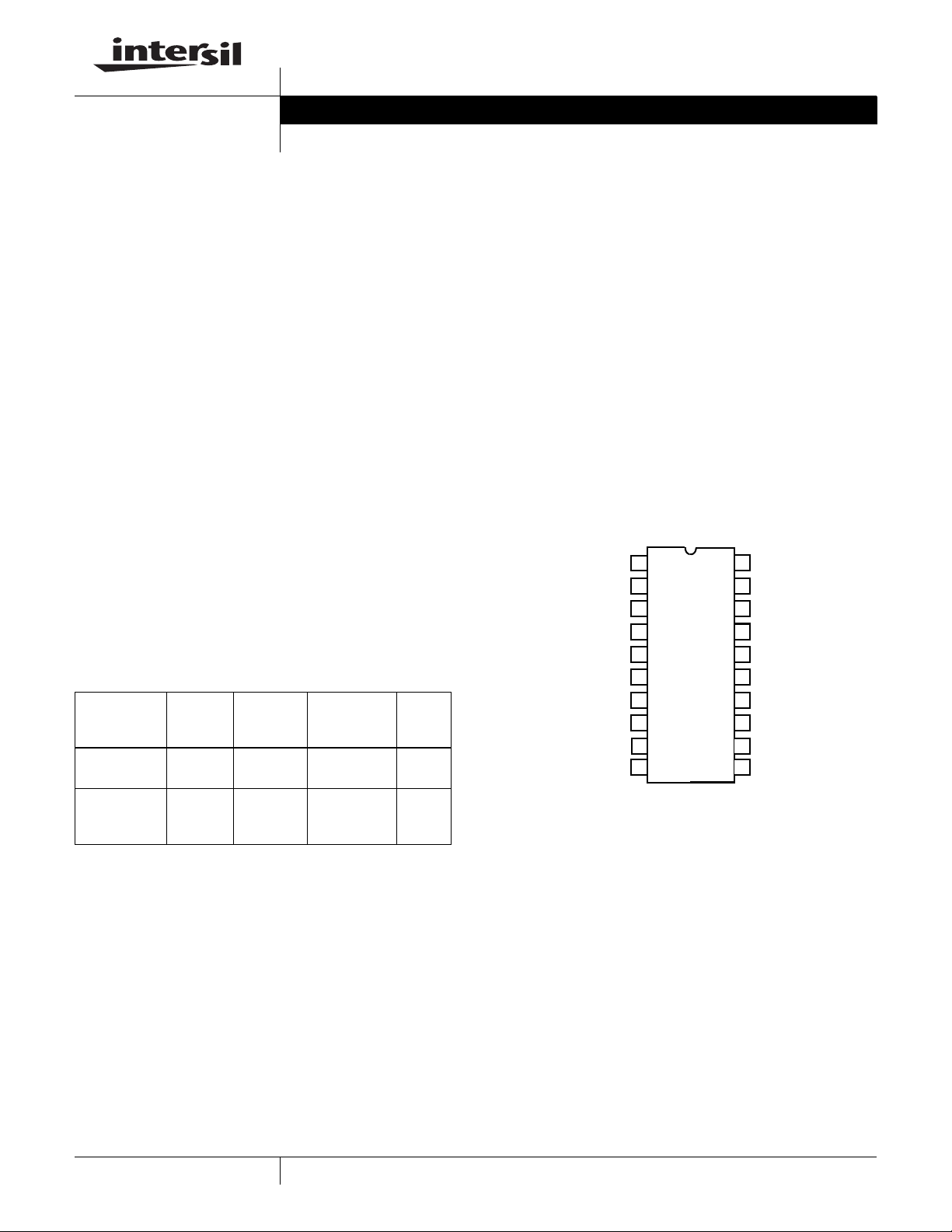
Pinout
20 Ld TSSOP
TOP VIEW
V
GND
IN1
IN2
IN3
IN4
IN5
IN6
IN7
OFF
1
2
3
4
5
6
7
8
9IN8
10V
20
ON1
OUT1
19
18
OUT2
17
OUT3
16
OUT4
15
OUT5
OUT6
14
OUT7
13
OUT8
12
11
V
ON2
1
CAUTION: These devices are sensitive to electrostatic discharge; follow proper IC Handling Procedures.
1-888-INTERSIL or 1-888-468-3774
| Intersil (and design) is a registered trademark of Intersil Americas Inc.
All other trademarks mentioned are the property of their respective owners.
Copyright © Intersil Americas Inc. 2005. All Rights Reserved.
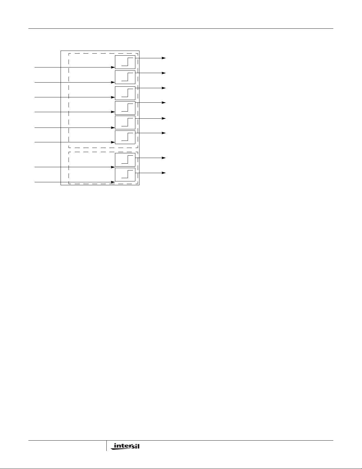
Functional Diagram
ISL24010
IN1
IN2
IN3
IN4
IN5
IN6
IN7
IN8
Connected to V
and V
OFF
Connected to V
and V
OFF
ON1
ON2
CH1
CH2
CH3
CH4
CH5
CH6
CH7
CH8
OUT1
OUT2
OUT3
OUT4
OUT5
OUT6
OUT7
OUT8
2
ISL24010
Absolute Maximum Ratings (T
Driver Positive Supply Voltage Range, (VON) . . . . . . . .+5V to +40V
Power Supply Voltage Range, (V
Negative Supply Voltage Range, (V
Supply Turn-on Slew Rate . . . . . . . . . . . . . . . . . . . . . . . . . . 10V/µs
Input Voltage Range, All Inputs . . . . . . . . . . . . . . . . . . -0.5V to 5.5V
Output Voltage Range, All Outputs . . . . . V
CAUTION: Stresses above those listed in “Absolute Maximum Ratings” may cause permanent damage to the device. This is a stress only rating and operation of the
device at these or any other conditions above those indicated in the operational sections of this specification is not implied.
ON
= 25°C) Thermal Information
A
Thermal Resistance (Typical, Note 1)
to V
OFF
) . . . . . .+10V to +60V
OFF
). . . . . . . . . . . . .-20V to -5V
-0.5V to VON +0.5V
OFF
20 Ld TSSOP Package . . . . . . . . . . . . . . . . . . . . . . 140
(continuous, all 8 channels) . . . . . . . . . . . . . . . . . . . . . . 80mA
I
OUT
T
AMBIENT
T
JUNCTION
T
STORAGE
. . . . . . . . . . . . . . . . . . . . . . . . . . . . . . . . . -40°C to +85°C
. . . . . . . . . . . . . . . . . . . . . . . . . . . . . . . -40°C to +150°C
. . . . . . . . . . . . . . . . . . . . . . . . . . . . . . . . -65°C to +150°C
θ
JA
(°C/W)
NOTE:
is measured with the component mounted on a HIGH effective thermal conductivity test board in free air. See Tech Brief TB379 for details.
1. θ
JA
IMPORTANT NOTE: All parameters having Min/Max specifications are guaranteed. Typical values are for information purposes only. Unless otherwise noted, all tests
are at the specified temperature and are pulsed tests, therefore: T
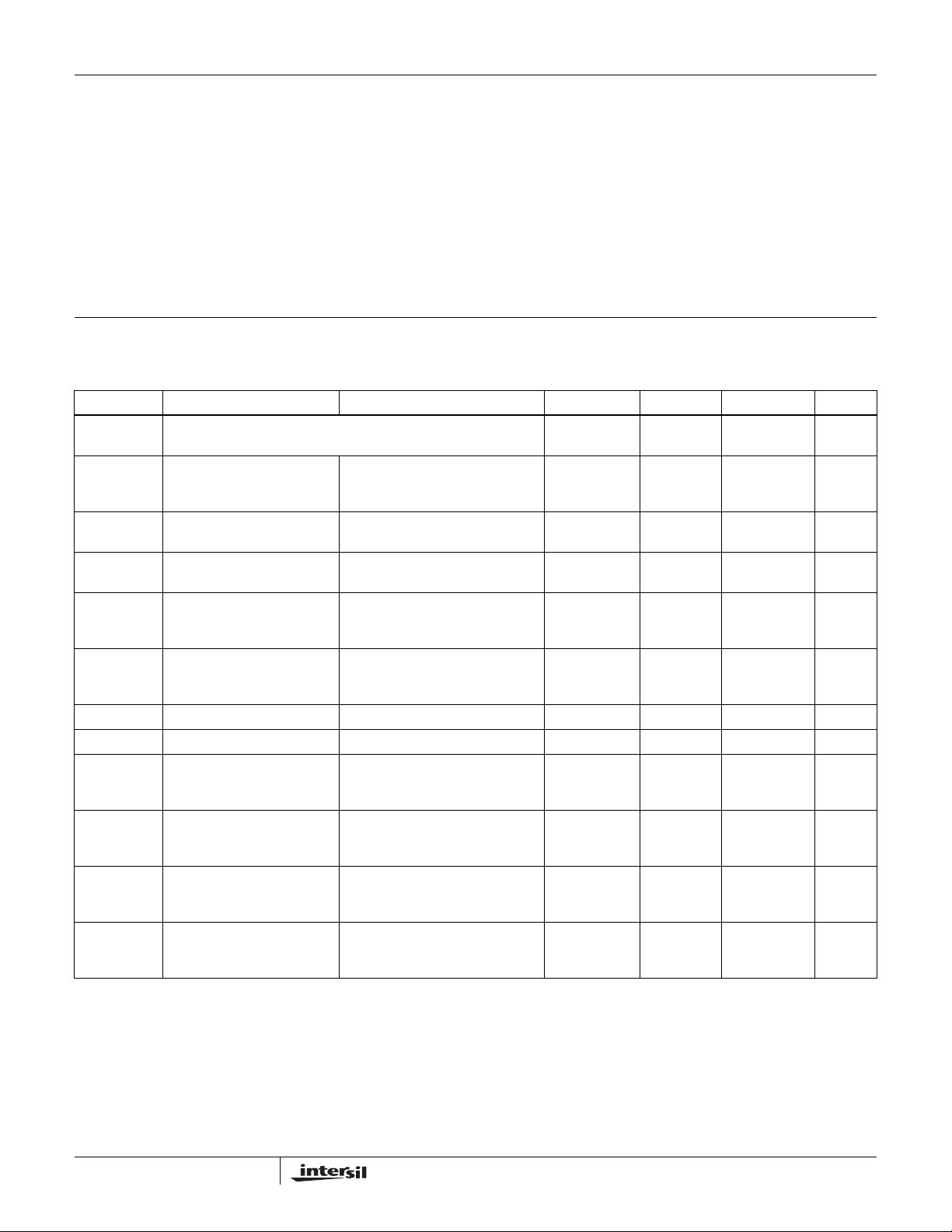
Electrical Specifications V
ON
= 22V, V
OFF
= TC = T
J
A
= -5V, TA = -40°C to +85°C Unless Otherwise Specified. Typical values tested at 25°C
PARAMETER DESCRIPTION CONDITION MIN TYP MAX UNIT
Power
Supplies
I(VON) Supply Current All Inputs low or high
Recommended Operating Voltages -5
(V
OFF
22
)
(VON)
V
1.8 4.0 mA
No load
V
= V
ON1
+ V
ON2
-4.0 -1.8 mA
-8.0 ± 2.0 8.0 µA
ON
) Supply Current All Inputs low or high
I(V
OFF
I
IN
Input Leakage Each Input low or high
No load
High = 1.8V, Low = 0.8V
VOH High Level Output Voltage IOH = -100µA
V
= 22V
ON
(V
- 1.5V) 21.2 V
ON
RL = 100pF in parallel with 5kΩ
VOL Low Level Output Voltage IOH = +100µA
V
= -5V
OFF
-4.3 (V
+ 1.5V) V
OFF
RL = 100pF in parallel with 5kΩ
VIH High Level Input Voltage 1.8 V
VIL Low Level Input Voltage 0.8 V
tplh Low to High Prop Delay 50% to 50%, Tested with
300 500 ns
RL = 100pF in parallel with 5kΩ,
f = 50kHz
tphl High to Low Prop Delay Measured at 50% to 50%
250 500 ns
f = 50kHz
RL = 100pF in parallel with 5kΩ,
ttlh Rise Time Measured at 10% to 90%
150 500 ns
f = 50kHz
RL = 100pF in parallel with 5kΩ
tthl Fall Time Measured at 10% to 90%
210 500 ns
f = 50kHz
RL = 100pF in parallel with 5kΩ
3

Pin Descriptions
ISL24010
PIN NUMBER
TSSOP-20 PIN NAME
EQUIVALENT
CIRCUIT DESCRIPTION
1 GND 4 Ground pin
2 IN1 1 Level shifter input 1
3 IN2 1 Level shifter input 2
4 IN3 1 Level shifter input 3
5 IN4 1 Level shifter input 4
6 IN5 1 Level shifter input 5
7 IN6 1 Level shifter input 6
8 IN7 1 Level shifter input 7
9 IN8 1 Level shifter input 8
10 VOFF 4 Negative output supply for all channels
11 VON2 4 Positive output supply for channels 7 and 8. V
V
.
ON1
12 OUT8 3 Lever shifter output 8
13 OUT7 3 Lever shifter output 7
14 OUT6 2 Lever shifter output 6
15 OUT5 2 Lever shifter output 5
16 OUT4 2 Lever shifter output 4
17 OUT3 2 Lever shifter output 3
18 OUT2 2 Lever shifter output 2
19 OUT1 2 Lever shifter output 1
20 VON1 4 Positive output supply for channels 1 through 6. V
V
.
ON2
V
V
ON2
OFF
Outputs 1-6 Outputs 7-8
IN
CIRCUIT 1.
V
OUT
V
CIRCUIT 2.
ON1
OFF
is required to be greater than or equal to
ON2
is required to be less than or equal to
ON1
V
ON2
OUT
V
OFF
CIRCUIT 3.
V
ON2
V
V
ON1
OFF
ESD CLAMP
CIRCUIT 4.
GND
4

ISL24010
Typical Performance Curves T
10.0
9.0
8.0
7.0
V
& 2 = 22V
ON1
V
= -5V
OFF
Input 50% Duty Cycle
10 15 20 25 30 35 40 45 50 55 60 65 70 75 80
FREQUENCY (kHz)
mA
6.0
5.0
4.0
3.0
2.0
1.0
0.0
= 25°C, Output load parallel RC (RL = 5kΩ, CL = 100pF) unless otherwise specified.
A
V
OFF
V
ON1
V
ON2
FIGURE 1. SUPPLY CURRENT vs FREQUENCY 1 CHANNEL
TOGGELING
15.0
13.5
12.0
V
& 2 = 22V
ON1
10.5
V
= -5V
OFF
9.0
mA
Input 50% Duty Cycle
7.5
6.0
4.5
3.0
1.5
0.0
10 15 20 25 30 35 40 45 50 55 60 65 70 75 80
FREQUENCY (kHz)
V
OFF
V
ON1
V
ON2
12.0
10.8
9.6
8.4
7.2
mA
6.0
V
& 2 = 22V
ON1
4.8
V
= -5V
OFF
3.6
Input 50% Duty Cycle
2.4
1.2
0.0
10 15 20 25 30 35 40 45 50 55 60 65 70 75 80
FREQUENCY (kHz)
V
ON1
V
OFF
FIGURE 2. SUPPLY CURRENT vs FREQUENCY
4 CHANNELS TOGGELING
15.0
13.5
12.0
V
& 2 = 22V
ON1
10.5
V
= -5V
OFF
9.0
Input 50% Duty Cycle
7.5
mA
6.0
4.5
3.0
1.5
0.0
10 15 20 25 30 35 40 45 50 55 60 65 70 75 80
FREQUENCY (kHz)
V
ON1
V
OFF
V
V
ON2
ON2
FIGURE 3. SUPPLY CURRENT vs FREQUENCY
6 CHANNELS TOGGLING
350
315
280
245
210
175
ns
140
V
& 2 = 20-40V
ON1
105
V
= -5V
OFF
70
Frequency 50kHz
35
100pF load
0
20 22 24 26 28 30 32 34 36 38 40
V
ON1
Prop Delay
& V
ON2
Fall Time
Rise Time
(V D.C.)
FIGURE 5. RISE TIME, FALL TIME AND PROP DELAY vs
V
ON1
& V
VOLTAGE WITH V
ON2
OFF
= -5V
FIGURE 4. SUPPLY CURRENT vs FREQUENCY
8 CHANNELS TOGGLING
ns
350
315
280
245
210
175
140
105
70
35
0
Prop Delay
Fall Time
Rise Time
V
= 20-40V
ON1 & 2
V
= -20V
OFF
Frequency 50kHz
100pF load
20 22 24 26 28 30 32 34 36 38 40
V
& V
ON2
(V D.C.)
ON1
FIGURE 6. RISE TIME, FALL TIME AND PROP DELAY vs
V
ON1
& V
VOLTAGE WITH V
ON2
OFF
= -20V
5

ISL24010
Typical Performance Curves T
2000
V
= 20-40V
ON1 & 2
1800
V
= -5V
OFF
1600
50kHz 50% Duty Cycle
1400
1200
1000
ns
800
600
400
200
0
20 22 24 26 28 30 32 34 36 38 40
V
& V
ON1
ON2
= 25°C, Output load parallel RC (RL = 5kΩ, CL = 100pF) unless otherwise specified. (Continued)
A
3300pF
1800pF
(V D.C.)
FIGURE 7. RISE TIME vs CAPACITANCE vs SUPPLY
VOLTAGE WITH V
2000
V
& 2 = 20-40V
ON1
1800
V
= -5V
OFF
50kHz 50% Duty Cycle
1600
1400
1200
1000
ns
800
600
400
200
0
20 22 24 26 28 30 32 34 36 38 40
V
ON1
OFF
& V
= -5V
ON2
3300pF
1800pF
(V D.C.)
100pF
100pF
2100
1890
ON1
& V
3300pF
(V D.C.)
ON2
1800pF
1680
1470
1260
1050
ns
840
V
& 2 = 20-40V
ON1
630
V
= -20V
OFF
420
50kHz 50% Duty Cycle
210
0
20 22 24 26 28 30 32 34 36 38 40
V
FIGURE 8. RISE TIME vs CAPACITANCE vs SUPPLY
VOLTAGE WITH V
2200
1980
1760
1540
1320
1100
ns
880
V
& 2 = 20-40V
ON1
660
V
= -20V
OFF
50kHz 50% Duty Cycle
440
220
0
20 22 24 26 28 30 32 34 36 38 40
V
ON1
OFF
& V
= -20V
3300pF
(V D.C.)
ON2
1800pF
100pF
100pF
FIGURE 9. FALL TIME vs CAPACITANCE vs SUPPLY
VOLTAGE WITH V
1500
1350
V
& 2 = 20-40V
ON1
V
= -5V
OFF
50kHz 50% Duty Cycle
20 22 24 26 28 30 32 34 36 38 40
V
ns
1200
1050
900
750
600
450
300
150
0
ON1
OFF
& V
= -5V
ON2
3300pF
1800pF
100pF
(V D.C.)
FIGURE 11. PROP DELAY vs CAPACITANCE vs SUPPLY
VOLTAGE WITH V
OFF
= -5V
6
FIGURE 10. FALL TIME vs CAPACITANCE vs SUPPLY
VOLTAGE WITH V
1500
V
& 2 = 20-40V
ON1
1350
V
= -5V
OFF
50kHz 50% Duty Cycle
1200
1050
900
750
ns
600
450
300
150
0
20 22 24 26 28 30 32 34 36 38 40
V
ON1
OFF
& V
= -20V
(V D.C.)
ON2
3300pF
1800pF
100pF
FIGURE 12. PROP DELAY vs CAPACITANCE vs SUPPLY
VOLTAGE WITH V
OFF
= -20V

ISL24010
Typical Performance Curves T
FIGURE 13. TRANSIENT RESPONSE vs LOAD CAPACITANCE
= 25°C, Output load parallel RC (RL = 5kΩ, CL = 100pF) unless otherwise specified. (Continued)
A
2V/DIV
0
100pF
5V/DIV
0
Pulse Input
1500pF
V
& 2 = 22V
ON1
V
= -5V
OFF
50kHz 50% Duty Cycle
Application Information
General
The ISL24010 is an Octal voltage level shifter. The part was
designed to level shifts a digital input signal to +22V and -5V
for TFT-LCD displays. The device is capable of level shifting
a CMOS logic signal between +40V and -20V.
Power Supply Decoupling
The ISL24010 requires a 0.1µF decoupling capacitor as
close to the V
large load equal to 5kΩ in parallel with 100pF (Figure 16).
This will deduce any dv/dt between the different supplies and
prevent the internal ESD clamp from turning on and
damaging the part.
ON1
, V
ON2
and V
power supply pins for a
OFF
2µs/DIV
Input Pin Connections
Unused inputs must be tied to ground. Failure to tie unused
input pins to ground will result in a rail to rail oscillations on
the respective output pins and higher unwanted power
dissipation in the part. Under these conditions, the
temperature of the part could get very hot.
Limiting the Output Current
No output short circuit current limit exists on this part. All
applications need to limit the output current to less than
80mA. Adequate thermal heat sinking of the parts is also
required.
Application Diagram (TV)
Power Supply Sequence
The ISL24010 requires that V
V
at all times. Therefore, if V
ON1
supplies, then V
needs to be turned on before V
ON2
The reason for this requirement is shown in Circuit 4 in the
Pin Description Table. The ESD protection diode between
V
and Von 1 will forward bias if V
ON2
drop greater than V
sequence: V
ON2
. Recommended power supply
ON2
, V
, V
ON1
The ESD protection scheme is based on diodes from the
pins to the V
supply and a dV/dt- triggered clamp. This
ON2
dV/dt triggered clamp imposes a maximum supply turn-on
slew rate of 10V/µs. This clamp will trigger if the supply
powers up too fast, causing amps of current to flow. Ground
and V
are treated as I/O pins with this protection
ON1
scheme. In applications where the dV/dt supply ramp could
exceed 10V/µs, such as hot plugging, additional methods
should be employed to ensure the rate of rise is not
exceeded.
be greater than or equal to
ON2
OFF
and Von 2 are different
ON1
becomes a diode
ON1
then input logic signals.
ON1
.
Latch-up Proof
The ISL24010 is manufactured in a high voltage DI process
that isolates every transistor in it’s own tub making the part
latch-up proof.
DC/DC
CONVERTER
1.0µF
1.0µF
TIMING
CON-
TROLLER
FIGURE 14. TYPICAL TV APPLICATION CIRCUIT
V
ON1
ISL24010
LEVEL
SHIFTER
V
ON2
V
OFF
1.0µF
LCD PANEL
7

Application Diagram (Monitor)
ISL24010
V
OFF
ISL24010
LEVEL
SHIFTER
VON SLICER
CIRCUIT
V
ON1
V
ON2
1.0µF
LCD PANEL
DC/DC
CONVERTER
V
OFF
1.0µF
TIMING
CON-
TROLLER
1.0µF
V
ON1VON1
V
ON2
FIGURE 15. TYPICAL MONITOR APPLICATION CIRCUIT WITH
SLICER TO REDUCE FLICKER
Test Circuit
V
ON1
V
ON2
OUT8
C
3
C
2
5kΩ 100pF
1.0µF
IN1
IN8
V
C
OFF
1
ISL24010
1.0µF
OUT1
1.0µF
If the output load is a series 200Ω resistor and a 3300pF
then C1, C2 and C3 can be reduced to 0.47pF.
INx
t
PHL
t
F
OUTx
t
PLH
t
R
FIGURE 16. TEST LOAD AND TIMING DEFINITIONS
8

ISL24010
Thin Shrink Small Outline Plastic Packages (TSSOP)
N
INDEX
AREA
123
-A-
0.05(0.002)
D
SEATING PLANE
e
b
0.10(0.004) C AM BS
M
E1
-B-
A
-C-
0.25(0.010) BM M
E
α
A1
0.10(0.004)
GAUGE
PLANE
0.25
0.010
A2
L
c
NOTES:
1. These package dimensions are within allowable dimensions of
JEDEC MO-153-AC, Issue E.
2. Dimensioning and tolerancing per ANSI Y14.5M-1982.
3. Dimension “D” does not include mold flash, protrusions or gate burrs.
Mold flash, protrusion and gate burrs shall not exceed 0.15mm
(0.006 inch) per side.
4. Dimension “E1” does not include interlead flash or protrusions. Interlead flash and protrusions shall not exceed 0.15mm (0.006 inch) per
side.
5. The chamfer on the body is optional. If it is not present, a visual index
feature must be located within the crosshatched area.
6. “L” is the length of terminal for soldering to a substrate.
7. “N” is the number of terminal positions.
8. Terminal numbers are shown for reference only.
9. Dimension “b” does not include dambar protrusion. Allowable dambar
protrusion shall be 0.08mm (0.003 inch) total in excess of “b” dimension at maximum material condition. Minimum space between protrusion and adjacent lead is 0.07mm (0.0027 inch).
10. Controlling dimension: MILLIMETER. Converted inch dimensions
are not necessarily exact. (Angles in degrees)
M20.173
20 LEAD THIN SHRINK SMALL OUTLINE PLASTIC
PACKAGE
INCHES MILLIMETERS
SYMBOL
A - 0.047 - 1.20 A1 0.002 0.006 0.05 0.15 A2 0.031 0.051 0.80 1.05 -
b 0.0075 0.0118 0.19 0.30 9
c 0.0035 0.0079 0.09 0.20 -
D 0.252 0.260 6.40 6.60 3
E1 0.169 0.177 4.30 4.50 4
e 0.026 BSC 0.65 BSC -
E 0.246 0.256 6.25 6.50 -
L 0.0177 0.0295 0.45 0.75 6
N20 207
o
α
0
o
8
o
0
o
8
Rev. 1 6/98
NOTESMIN MAX MIN MAX
-
All Intersil U.S. products are manufactured, assembled and tested utilizing ISO9000 quality systems.
Intersil Corporation’s quality certifications can be viewed at www.intersil.com/design/quality
Intersil products are sold by description only. Intersil Corporation reserves the right to make changes in circuit design, software and/or specifications at any time without
notice. Accordingly, the reader is cautioned to verify that data sheets are current before placing orders. Information furnished by Intersil is believed to be accurate and
reliable. However, no responsibility is assumed by Intersil or its subsidiaries for its use; nor for any infringements of patents or other rights of third parties which may result
from its use. No license is granted by implication or otherwise under any patent or patent rights of Intersil or its subsidiaries.
For information regarding Intersil Corporation and its products, see www.intersil.com
9
 Loading...