

查询ISL24006供应商
®
ISL24006
Data Sheet September 9, 2005
14-Channel Programmable Switchable I2C
TFT-LCD Reference Voltage Generator
with Integrated 4-Channel Static Gamma
Drivers
The ISL24006 is a 14-channel programmable switchable
reference voltage generator with four channels of static
gamma drivers integrated, for a complete 18-channel total
gamma solution for TFT-LCD displays. The 14-channel
programmable switchable configuration allows switching
between two gamma curves.
The ISL24006 is divided into two banks of seven generators:
one designed to cover the range from V
the remaining seven channels covering the range from
V
REFU_L
to V
REFU_H
. Each bank has its own separate high
and low reference inputs, with integrated buffers (four static
gamma drivers) to drive the column driver internal DAC
resistor string to within 0.2V from the top and bottom rails.
An output MUX is used to switch between the two curves in
less than 1µs. Switching is controlled using an external
select pin.
ISL24006 includes an I
2
C interface for programming the
offset values.
REFL_L
to V
REFL_H
FN6110.1
Features
• 14-channel programmable switchable
• 4-channel static
• Fast switch time (< 1µs)
• Programmable with 20mV resolution
• Digital supply 3.3V to 5V
• Supply current of 32mA (without load)
• Rail-to-Rail capability
2
C interface
;
•I
• Pb-free plus anneal available (RoHS compliant)
Applications
• TFT-LCD drive circuits
• Reference voltage generators
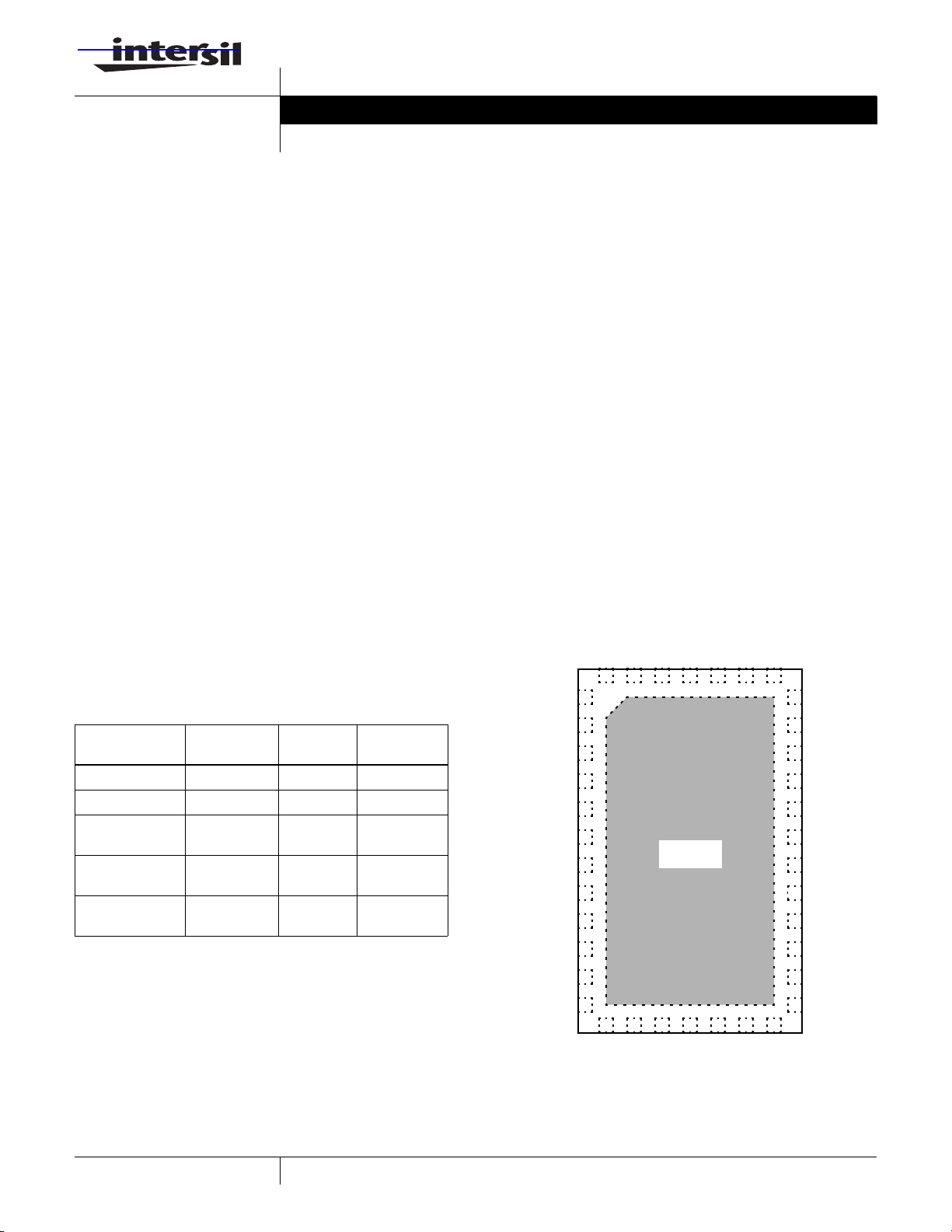
Pinout
ISL24006
(38-PIN QFN)
TOP VIEW
ISL24006 is available in the 38-pin QFN package and is
specified for operation over the -40°C to +85°C temperature
range.
Ordering Information
PAR T
NUMBER PACKAGE
ISL24006IR-T7 38-Pin QFN 7” MDP0046
ISL24006IR-T13 38-Pin QFN 13” MDP0046
ISL24006IRZ
(See Note)
ISL24006IRZ-T7
(See Note)
ISL24006IRZ-T13
(See Note)
NOTE: Intersil Pb-free plus anneal products employ special Pb-free
material sets; molding compounds/die attach materials and 100%
matte tin plate termination finish, which are RoHS compliant and
compatible with both SnPb and Pb-free soldering operations. Intersil
Pb-free products are MSL classified at Pb-free peak reflow
temperatures that meet or exceed the Pb-free requirements of
IPC/JEDEC J STD-020.
38-Pin QFN
(Pb-Free)
38-Pin QFN
(Pb-Free)
38-Pin QFN
(Pb-Free)
TAPE &
RE E L PK G. D WG. #
- MDP0046
7” MDP0046
13” MDP0046
OUT_REFU_H
AVD D
STD_REG
A0
SDA
SCL
OSC
DVDD
BANK_SEL
NC
GND
OUT_REFL_L
OUT1
OUT2
OUT3
OUT4
OUT5
OUT6
OUT7
38
37
36
35
34
33
32
1
2
3
4
5
6
7
8
9
10
11
12
13
OUT14
14
OUT13
THERMAL
PAD
15
16
OUT11
OUT12
17
OUT10
18
OUT9
31
OUT_REFU_L
30
GND
29
BG
28
GND
27
VREFL_L
26
VREFL_H
25
NC
24
NC
23
VREFU_L
22
VREFU_H
21
AVDD
20
OUT_REFL_H
19
OUT8
1
CAUTION: These devices are sensitive to electrostatic discharge; follow proper IC Handling Procedures.
1-888-INTERSIL or1-888-468-3774
| Intersil (and design) is a registered trademark of Intersil Americas Inc.
All other trademarks mentioned are the property of their respective owners.
Copyright © Intersil Americas Inc. 2005. All Rights Reserved.
ISL24006
Absolute Maximum Ratings (T
Supply Voltage between A
Supply Voltage between D
Maximum Continuous Output Current . . . . . . . . . . . . 20mA/channel
Operating Temperature . . . . . . . . . . . . . . . . . . . . . . .-40°C to +85°C
CAUTION: Stresses above those listed in “Absolute Maximum Ratings” may cause permanent damage to the device. This is a stress only rating and operation of the
device at these or any other conditions above those indicated in the operational sections of this specification is not implied. The device outputs cannot withstand shortcircuit condition for extended periods of time. To avoid damage, do not exceed absolute maximum rating of 20mA/channel.
IMPORTANT NOTE: All parameters having Min/Max specifications are guaranteed. Typ values are for information purposes only. Unless otherwise noted, all tests are
at the specified temperature and are pulsed tests, therefore: T
and GND . . . . . . . . . . . . . . . . .+18V
VDD
and GND lesser of VS or +7V (max)
VDD
Electrical Specifications A
= 25°C)
A
= 15V, D
VDD
C
= 10pF to 1/2 A
L
Power Dissipation . . . . . . . . . . . . . . . . . . . . . . . . . . . . . . . . . . . TBD
Maximum Die Temperature . . . . . . . . . . . . . . . . . . . . . . . . . . +125°C
Lead Temperature . . . . . . . . . . . . . . . . . . . . . . . . . . . . . . . . . +260°C
Storage Temperature . . . . . . . . . . . . . . . . . . . . . . . . -65°C to +150°C
= TC = T
J
VDD
VDD
A
= 5V, V
REFU_H
, TA = 25°C, unless otherwise specified.
= 14V, V
REFU_L
= 8.5V, V
REFL_H
= 6.5V, V
= 1V, RL = 1kΩ and
REFL_L
PARAMETER DESCRIPTION CONDITIONS MIN TYP MAX UNIT
SUPPLY
I
AVD D
I
DVDD
Supply Current No load 30 38 mA
Digital Supply Current 2.75 4 mA
ANALOG
V
OH
V
OL
V
OH
V
OL
PSRR Power Supply Rejection Ratio A
V
AC
I
B
REG Load Regulation I
OUT1 to OUT7 V
OUT1 to OUT7 V
OUT8 to OUT14 V
OUT8 to OUT14 V
= 14V, A
REFU_H
= 8.5V, A
REFU_L
= 6.5V, A
REFL_H
= 1.0V, A
REFL_L
is moved from 14V to 16V 42 50 dB
VDD
= 15V 13.94 13.98 14.02 V
VDD
= 15V 8.47 8.51 8.55 V
VDD
= 15V 6.44 6.48 6.52 V
VDD
= 15V 0.96 1.00 1.04 V
VDD
Accuracy -50 0 +50 mV
Input Bias Current,
V
REF(U_H, U_L, L_H, L_L)
V
= 1/2 A
REF
OUT
VDD
= 5mA step 0.5 mV/mA
250nA
BG Band Gap 1.1 1.3 1.4 V
SR Slew Rate 815 V/µs
t
S
Settling Time ±1/2 LSB 1 µs
DIGITAL
V
V
F
R
t
S
t
H
IH
IL
CLK
SDIN
Logic 1 Input Voltage D
Logic 0 Input Voltage 20%*
VDD
20%
-
V
V
D
VDD
Clock Frequency 400 kHz
S
Input Resistance SCL, SDA, STD_REG 1 GΩ
DIN
Setup Time 40 ns
Hold Time 40 ns
2
FN6110.1
September 9, 2005
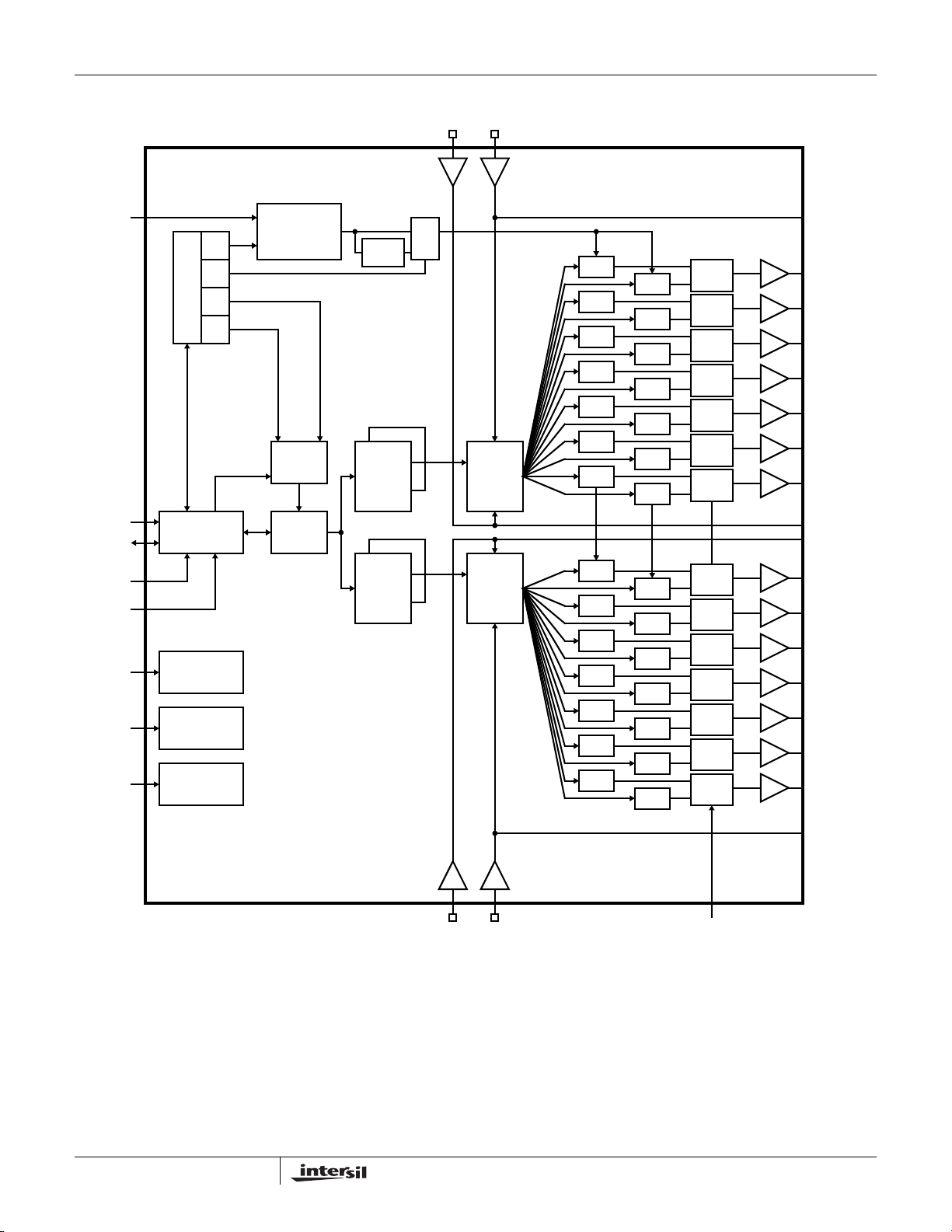
Block Diagram
ISL24006
VREFU_HVREFU_L
OSC
SCL
SDA
STD_REG
A0
AVDD
DVDD
BG
C3
C0
C1
CONTROL
C2
I2C
INTERFACE
ANALOG
POWER
DIGITAL
POWER
REFERENCE
GENERATOR
INT/EXT
OSCILLATOR
MUX
MUX
DELAY
BANKA
HI
BANKA
LO
0
1
B
DAC HI
B
DAC LO
S/H
S/H
S/H
S/H
S/H
S/H
S/H
S/H
S/H
S/H
S/H
S/H
S/H
S/H
S/H
S/H
S/H
S/H
S/H
S/H
S/H
S/H
S/H
S/H
S/H
S/H
S/H
S/H
MUX
MUX
MUX
MUX
MUX
MUX
MUX
MUX
MUX
MUX
MUX
MUX
MUX
MUX
OUT REFU_H
OUT1
OUT2
OUT3
OUT4
OUT5
OUT6
OUT7
OUT REFU_L
OUT REFL_H
OUT8
OUT9
OUT10
OUT11
OUT12
OUT13
OUT14
OUT REFL_L
VREFL_H VREFL_L
3
BANK_SEL
FN6110.1
September 9, 2005

ISL24006
Pin Descriptions
PIN NUMBER PIN NAME PIN TYPE PIN FUNCTION
1 OUT REFU_H Analog Output Analog output of V
2, 21 AVDD Analog Power Power supply for analog circuit
3 STD_REG Logic Input Selects mode, high = standard, low = register
2
4 A0 Logic Input I
5 SDA Input/Output I
6 SCL Logic Input I
7 OSC Input/Output Input clock reference
8 DVDD Digital Power Power supply for digital circuit
9 BANK_SEL Digital Signal Select one of two sets of gamma voltages
10, 24, 25 NC Not connected
28, 30, 11 GND GND Ground
12 OUT REFL_L Analog Output Analog output of V
13, 14, 15, 16, 17,
18, 19
20 OUT REFL_H Analog Output Analog output of V
22 VREFU_H Reference High reference for upper seven output voltages
23 VREFU_L Reference Low reference for upper seven output voltages
26 VREFL_H Reference High reference for lower seven output voltages
27 VREFL_L Reference Low reference for lower seven output voltages
29 BG Analog Bypass Pin Decoupling capacitor for internal reference generator
31 OUT REFU_L Analog Output Analog output of V
32, 33, 34, 35, 36,
37, 38
OUT8 - OUT14 Analog Output Analog output voltages in lower range
OUT1 - OUT7 Analog Output Analog output voltages in upper range
C device address input, bit 0; when LO, hex address = 74; when HI, hex
address = 75
2
C data
2
C clock
REFU_H
REFL_L
REFL_H
REFU_L
4
FN6110.1
September 9, 2005

A
A
A
A
X
X
X
A
AAA
A
A
A
A
X
X
X
A
A
A
A
A
A0RA
A
A
A
A
A
14
Data 12
ISL24006
NA
14
STOP
N
Data 2 Data 3
Data 1Control Byte
= don't care
Device Address
AAAA A
A6 A5 A4 A3 A2 A1 A0 W A C7 C6 C5 C4 C3 C2 C1 C0 A D7 D6 D5 D4 D3 D2 D1 D0 A D7 D6 D5 D4 D3 D2 D1 D0 A D7 D6 D5 D2 D1 D0 A
123456789123456789123456789123456789123 6789
Data 3 Data 12 Stop
Data 2
Data 1
Device Address
DAT
STOP
R
DAT
D7 D6 D5 D4 D3 D2 D1 D0
D7 D6 D5 D4 D3 D2 D1 D0
1
2
3
4
5
6
C TIMING DIAGRAM 1
2
FIGURE 1. I
R3 R2 R1 R0
Register Address
A D7D6D5D4D3D2D1D0 A D7D6D5D4D3D2D1D0 A D7D6D5 D2D1D0 A
0W
1
2
3
4
Device Address
5
A6 A5 A4 A3 A2 A1 A0 R A A A
123456789123456789123456789123 6789
6
123456789123456789123456789
R3 R2 R1 R0
0W
1
2
3
4
Device Address Register Address Device Address
5
6
1234567891234567891234567891234567891
Start WAAAA AStop
C DATA
2
C SDA In
I
2
I
C SDA Out
2
STANDARD MODE (STD/REG=HIGH) WRITE MODE
I
Start R A A A NA
C DATA
2
C CLK In
2
I
STANDARD MODE (STD/REG=HIGH) READ MODE
C SDA In
I
2
I
C SDA Out
2
I
Start W
C DATA
2
C CLK In
2
I
C SDA In
I
2
I
C SDA Out
2
REGISTER MODE (STD/REG=LO) WRITE MODE
I
5
Start W
C DATA
2
C CLK In
2
I
REGISTER MODE (STD/REG=LO) READ MODE
C SDA In
I
2
I
C SDA Out
2
I
C CLK In
2
I
FN6110.1
September 9, 2005

gg
ISL24006
General Description
The ISL24006 provides a versatile method of providing the
reference voltages that are used in setting the transfer
characteristics of LCD display panels. The V/T
(Voltage/Transmission) curve of the LCD panel requires that
a correction is applied to make it linear. However, if the panel
is to be used in more than one application, the final curve
may differ for different applications. By using the ISL24006,
the V/T curve can be changed to optimize its characteristics
according to the required application of the display product.
Each of the 14 reference voltage outputs can be set with a 8bit resolution. The first half of the output buffers, OUT1 to
OUT7 can be operated from V
REFU_L
second half OUT8 to OUT14 can swing from V
V
REFL_H
.
It is also possible to use the ISL24006 for applications other
than LCDs where multiple voltage references are required
that can be set to 8-bit accuracy.
Digital Interface
The ISL24006 uses a simple two-wire I2C interface to
program all 14 outputs. The bus line SCLK is the clock signal
line and bus SDA is the bi-directional data information signal
line. The ISL24006 can support a clock rate up to 400kHz.
An external pull up typically 1kΩ resistor is required for each
bus line.
to V
REFU_H
REFL_L
. The
to
Byte Format
Every byte put along the SDA line must be eight bits long.
The number of bytes that can be transmitted between a Start
and Stop condition is unrestricted. Data is always transferred
with the most significant bit (MSB) first.
Acknowledge
Each byte is followed by an acknowledge bit.
When a master device is sending data (WRITE) the master
puts a resistive high level on the SDA line during the
acknowledge clock pulse. The peripheral that
acknowledges, which is the receiver, has to pull down the
SDA line during the acknowledge pulse.
When a master device is receiving data (READ) the slave
puts a resistive high level on the SDA line during the
acknowledge clock pulse. The master will acknowledge by
pulling down the SDA line during the acknowledge pulse.
Not Acknowledge
A Not Acknowledge (NA) is when the receiver does not pull
down the SDA line during the acknowledge pulse: SDA line
remains in the HI or in a high impedance state.
A Not Acknowledge is the master device's signal to the slave
device to release the SDA line so the master device can
generate a Stop signal on the same line. The NA indicates
that data just received is the last byte of the data transfer.
Start and Stop Condition
A Start condition is a high to low transition on the serial data
line (SDA) line while the serial clock line (SCLK) holds high.
The Stop condition is a low to high transition on the SDA line
while SCLK is high. The master device always generates
Start and Stop conditions. The bus is considered to be busy
after the Start condition and to be free at a certain time
interval after the Stop condition. The two bus lines must be
high when the buses are not in use. The I
2
C Timing Diagram
2 (Figure 2) shows the format.
Data Validity
The data on the SDA line must be stable (clearly defined as
HI or LO) during the HI period of the clock signal. SDA
transition can only change when the clock signal on the
SCLK line is LO.
Start, Stop and Timing Details of I2C Interface
Sta rt Cond ition Data Clocke d in
SDA
DATA
SCL
CLO CK
t
tSt
S
H
FIGURE 2. I2C TIMING DIAGRAM 2
t
H
Stop Condition
t
R
Standard Mode
When pin #6 (STD_REG) is pulled high, the part operates in
Standard Mode, which is more commonly used than the
Register Mode. In the Standard Mode, the user can program
all outputs in one data stream or transfer frame.
For the Standard Mode in a WRITE transfer, a master device
sends data to program all the output buffers of the ISL24006.
The input data byte (DATA 1) to the first channel (OUT1) is
the third byte following the control byte. The second channel
(OUT2) is programmed by the fourth byte (DATA 2), and so
on. Each byte is followed by an acknowledge bit.
t
F
6
FN6110.1
September 9, 2005

ISL24006
TABLE 1. STANDARD MODE WRITE TRANSFER
S ISL24006 ADDRESS + W A CONTROL BYTE A DATA 1 A DATA 2 A ... DATA 14 A P
S = Start condition CONTROL BYTE = multifunction control
P = Stop condition DATA 1 = 8-bit input to DAC OUT1
A = Acknowledge bit DATA 2 = 8-bit input to DAC OUT2
DATA 14 = 8-bit input to DAC OUT14
For the Standard mode in a READ transfer, a master device
accepts data from the ISL24006. The output data byte
(DATA 1) of the first channel (OUT1) is the second byte of
the transfer. OUT2 output data byte is the third byte of the
transfer, and so forth and so on. The ISL24006 sends an
acknowledge bit after every eighth bit to tell the master
device that the ISL24006 is ready to send another byte.
Consequently, the master must send a Not Acknowledge,
(NA) at the end of the 14th data byte to tell ISL24006 to
release the SDA bus.
TABLE 2. Standard Mode READ Transfer
ISL24006
S
ADDRESS + R A DATA 1 A DATA 2 A ...
S = Start condition A = Acknowledge
P = Stop condition NA = Not Acknowledge
DATA 1 = 8-bit input to DAC OUT1
DATA 2 = 8-bit input to DAC OUT2
DATA 14 = 8-bit input to DAC OUT14
DATA
14 P
See Timing Diagram 1 (Figure 1) for detailed formats.
Devices Address and W/R Bit
Data transfers follow the format shown in Timing Diagram 1.
After the Start condition, a first byte is sent which contains
the Device Address and write/read bit. This address is a 7-bit
long device address and only two device addresses hex (74)
and hex (75) in binary, bin (111010) and bin (111011) are
allowed for the ISL24006. The first 6 bits (A6 to A1, MSBs) of
the device address have been factory programmed and are
always 111010. Only the least significant bit (LSB) A0 is
allowed to change the logic state. This LSB is controlled
externally on the pin #4, A0. When pulled high to D
LSB of the device address is high and thus the address is
hex (75) or in binary bin (1110101). When pulled low to GND,
the LSB of the device address low and thus the address is
hex (74) or in binary 1110100. Since the device address has
to be unique in the I
2
C bus line, a maximum of two ISL24006
may be used on the same bus at one time.
The ISL24006 monitors the bus continuously and waiting for
the Start condition followed by the device address. When the
device recognizes its device address, it will start to accept
data. The eighth bit (W/R) following the device address
indicates the data direction. A "0" is a Write transmission; a
master device will send data to the ISL24006 to set or
VDD
, the
program a desired reference voltage. A "1" indicates a Read
transmission; the master device will receive data from the
ISL24006 to read the previous data the voltage reference
was set or programmed.
Control Byte
The multi-function control byte contains information that
selects the memory bank (bankA, or bankB), and operation
(output, read, or write). It also controls the OSC pin function
(external or internal).
TABLE 3. Control Byte
C7 C6 C5 C4 C3 C2 C1 C0
XXXX0000
C0 = "0" bypass oscillator
= "1" 3.5µs lagging
C1 = "0" write data to bankA (default)
= "1" write data to bankB
C2 = "0" read data from bankA (default)
= "1" read data from bankB
C3 = "0" internal oscillator (default)
= "1" external oscillator
The second bit, C1, selects which bank to write to. A "0"
selects bankA. A "1" selects bankB. C1 is a "don't care" on
a read mode.
The third bit, C2, selects which bank to read from. A "0"
selects bankA. A "1" selects bankB. C2 is a "don't care" on
a write mode.
The fourth bit, C3, selects the function of the OSC pin. A "0"
selects the internal oscillator. When the internal oscillator is
selected, the OSC pin acts as an output pin. It generates a
square wave with a frequency of typically 20kHz where
multiple chips can be synchronized. A "1" selects an external
oscillator. When the external oscillator is selected, the OSC
pin acts an input pin. Multiple chips can be synchronized to
an external oscillator. The external frequency or refresh rate
can be synchronized up to 200kHz typically.
The rest of the bits (C4-C7) in the control byte are "don't
cares".
7
FN6110.1
September 9, 2005

Data Byte
Data Bytes are the input code data to the 8-bit DACs. Most
significant bits are clocked in first. These data bytes
determine the output voltages of the ISL24006.
b
7
10111010
b
6
b
5
b
4
ISL24006
TAB L E 4 .
b
3
b
2
b
1
b
0
271() 260() 251() 241() 231() 220() 211() 2
Ideal Transfer Function Example
Given a typical voltage applied to V
V
REF U_H
V
REF U_L
14V 8.5V–
R
----------------------------- 21.5m V==
BINARY INPUT DECIMAL VOUT1 (V) VOUT14 (V)
00000000 0 8.5 1
00000001 1 8.521484 1.021484
00000011 3 8.564453 1.064453
00000111 7 8.650391 1.150391
00001111 15 8.822266 1.322266
00011111 31 9.166016 1.666016
00111111 63 9.853516 2.353516
01111111 127 11.22852 3.728516
11111111 255 13.97852 6.478516
14V=
8.5V=
256
TAB L E 5 .
REFU_H
V
REF L_H
V
REF L_L
R
and V
REFU_L
6.5V=
1V=
6.5V 1V–
-------------------------- 21.5 mV==
256
0
0()×+×+×+×+×+×+×+×
For transient load application, the external clock mode
:
should be used to ensure all functions are synchronized
together. The positive edge of the external clock to the OSC
pin should be timed to avoid the transient load effect.
The Application Drawing shows the LCD H rate signal used,
here the positive clock edge is timed to avoid the transient
load of the column driver circuits. After power on, the chip
will default with the internal oscillator mode. At this time, the
OSC pin will be in a high impedance condition to prevent
contention.
Channel Outputs
Each of the channel outputs has a rail-to-rail buffer. This
enables all channels to have the capability to drive to within
50mV of the power rails (see Electrical Characteristics for
details).
When driving large capacitive loads, a series resistor should
be placed in series with the output. (Usually between 5Ω and
50Ω).
Each of the channels is updated on a continuous cycle. The
time for the new data to appear at a specific output will
depend on the exact timing relationship of the incoming data
to this cycle.
Clock Oscillator
The ISL24006 require an internal clock or external clock to
refresh its outputs. The outputs are refreshed at the falling
OSC clock edges. The output refreshed switches open at
the rising edges of the OSC clock. The driving load shouldn't
be changed at the rising edges of the OSC clock. Otherwise,
it will generate a voltage error at the outputs. This clock may
be input or output via the clock pin labelled OSC. The
internal clock is provided by an internal oscillator running at
approximately 21kHz and can be output to the OSC pin. In a
two-chip system, if the driving loads are stable, one chip may
be programmed to use the internal oscillator; then the OSC
pin will output the clock from the internal oscillator. The
second chip may have the OSC pin connected to this clock
source.
8
Power-On Sequencing
At power-on, make sure that A
the ESD diode between A
much current. If D
Do not ground A
VDD
VDD
VDD
comes on first, leave A
.
≥ D
VDD
and D
- 0.5V to prevent
VDD
from driving too
VDD
VDD
floating.
Power Dissipation
With the 30mA maximum continues output drive capability
for each channel, it is possible to exceed the 125°C absolute
maximum junction temperature. Therefore, it is important to
calculate the maximum junction temperature for the
application to determine if load conditions need to be
modified for the part to remain in the safe operation.
FN6110.1
September 9, 2005

The maximum power dissipation allowed in a package is
determined according to:
T
–
P
DMAX
JMAXTAMAX
---------------------------------------------=
Θ
JA
where:
ISL24006
•T
•T
• θ
•P
= Maximum junction temperature
JMAX
= Maximum ambient temperature
AMAX
= Thermal resistance of the package
JA
= Maximum power dissipation in the package
DMAX
The maximum power dissipation actually produced by the IC
is the total quiescent supply current times the total power
supply voltage and plus the power in the IC due to the loads.
P
DMAXAVDDIAVDD
Σ A([
VDDVOUT
i ) I
LOAD
i×– ]+×=
when sourcing, and:
P
DMAXAVDDIAVDD
Σ V
OUT
iI
LOAD
i×()+×=
when sinking.
Where:
• i = 1 to total 14
•A
•I
•V
•I
By setting the two P
can solve for the R
= Supply voltage
VDD
= Quiescent current
AVD D
i = Output voltage of the i channel
OUT
i = Load current of the i channel
LOAD
equations equal to each other, we
DMAX
s to avoid the device overheat. The
LOAD
package power dissipation curves provide a convenient way
to see if the device will overheat.
Power Supply Bypassing and Printed Circuit
Board Layout
Good printed circuit board layout is necessary for optimum
performance. A low impedance and clean analog ground
plane should be used for the ISL24006. The traces from the
two ground pins to the ground plane must be very short. The
thermal pad should be connected to the analog ground
plane. Lead length should be as short as possible and all
power supply pins must be well bypassed. A 0.1µF ceramic
capacitor must be placed very close to the A
V
REFU_L
, V
REFL_H
, V
, and BG pins. A 4.7µF local
REFL_L
bypass ceramic capacitor should be placed to the A
V
REFU_H
, V
REFU_L
, V
REFL_H
, V
REFL_L
9
VDD
pins.
, V
REFU_H
VDD
,
,
FN6110.1
September 9, 2005

Package Outline Drawing
ISL24006
NOTE: The package drawing shown here may not be the latest version. To check the latest revision, please refer to the Intersil website at
http://www.intersil.com/design/packages/index.asp
All Intersil U.S. products are manufactured, assembled and tested utilizing ISO9000 quality systems.
Intersil Corporation’s quality certifications can be viewed at www.intersil.com/design/quality
Intersil products are sold by description only. Intersil Corporation reserves the right to make changes in circuit design, software and/or specifications at any time without
notice. Accordingly, the reader is cautioned to verify that data sheets are current before placing orders. Information furnished by Intersil is believed to be accurate and
reliable. However, no responsibility is assumed by Intersil or its subsidiaries for its use; nor for any infringements of patents or other rights of third parties which may result
from its use. No license is granted by implication or otherwise under any patent or patent rights of Intersil or its subsidiaries.
For information regarding Intersil Corporation and its products, see www.intersil.com
10
FN6110.1
September 9, 2005
 Loading...