

®
www.BDTIC.com/Intersil
ISL23711
Volatile Digitally Controlled Potentiometer (XDCP™)
Data Sheet August 16, 2005
Terminal Voltage ±3V or ±5V, 128 Taps I2C
Serial Interface
The Intersil ISL23711 is a digitally controlled potentiometer
(XDCP). The device consists of a resistor array, wiper
switches, and a control section. The wiper position is
controlled by an I
2
C interface.
The potentiometer is implemented by a resistor array
composed of 127 resistive elements and a wiper switching
network. The wiper terminal can be connected to either end
of the resistor array or at any one of the Tap Positions in
between, providing 128 steps of resolution between R
R
. The “position” of the wiper is determined by the value
H
and
L
assigned to the volatile Wiper Register (WR). The WR can
be directly written to and read from using standard I
2
C
interface protocol. The device is available in either a 10kΩ or
50kΩ version.
The device can be used as a three-terminal potentiometer or
as a two-terminal variable resistor in a wide variety of
applications including:
• Industrial and Automotive Control
• Parameter and Bias Adjustments
• Amplifier Bias and Control
Ordering Information
TEMP
PAR T N UMBER
(BRAND)
ISL23711WIU10Z
(AOE) (Notes 1, 2)
ISL23711UIU10Z
(AOD) (Notes 1, 2)
NOTES:
1. Add “-T” suffix for tape and reel.
2. Intersil Pb-free plus anneal products employ special Pb-free material
sets; molding compounds/die attach materials and 100% matte tin plate
termination finish, which are RoHS compliant and compatible with both
SnPb and Pb-free soldering operations. Intersil Pb-free products are
MSL classified at Pb-free peak reflow temperatures that meet or
exceed the Pb-free requirements of IPC/JEDEC J STD-020.
RESISTANCE
OPTION (Ω)
10K -40 to +85 10 Ld MSOP
50K -40 to +85 10 Ld MSOP
RANGE
(°C) PACKAGE
PKG.
DWG. #
M10.118
(Pb-Free)
M10.118
(Pb-Free)
FN6127.0
Features
•I2C Serial Interface with Hardwire Slave Address Allows
up to Four Devices
• DCP Terminal Voltage, from V- to V
CC
• 127 Resistive Elements
- Typical R
- Typical ratiometric tempco ±4ppm/
tempco ±50ppm/°C
TOTAL
°C
- End to end resistance range ±20%
- Wiper resistance = 70Ω typ at V
CC
= 3.3V
• Low Power CMOS
- Standby current, 500nA max
- Active current, 200µA max
= 2.7V to 5.5V
-V
CC
- V- = -2.7V to -5.5V
•R
Values = 10kΩ, 50kΩ
TOTAL
• Volatile Wiper Storage
• Package
-10 Ld MSOP
• Pb-Free Plus Anneal Available (RoHS Compliant)
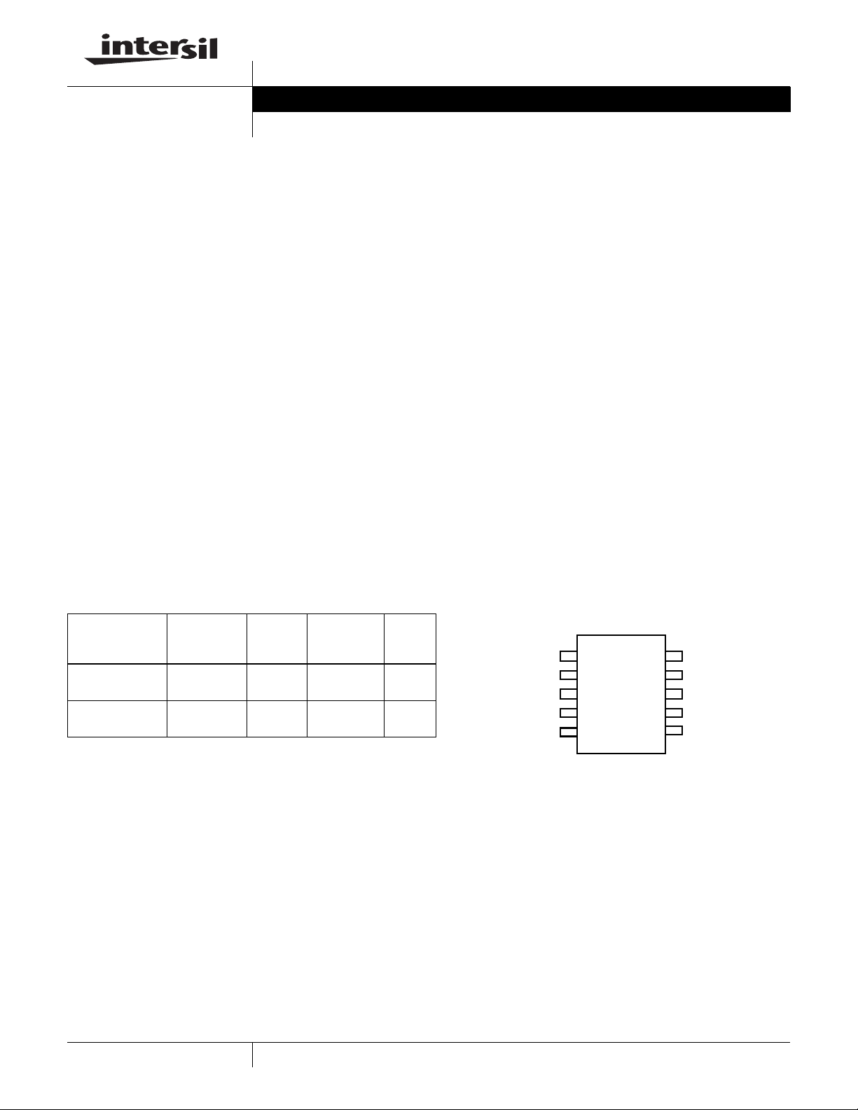
Pinout
ISL23711
(10 LD MSOP)
TOP VIEW
SDA
GND
A1
A0
1
V-
2
3
4
5
SCL
10
V
9
CC
R
8
L
R
W
7
6
R
H
1
CAUTION: These devices are sensitive to electrostatic discharge; follow proper IC Handling Procedures.
1-888-INTERSIL or 1-888-468-3774 | Intersil (and design) is a registered trademark of Intersil Americas Inc.
XDCP is a trademark of Intersil, Inc. Copyright Intersil Americas Inc. 2005. All Rights Reserved
All other trademarks mentioned are the property of their respective owners.
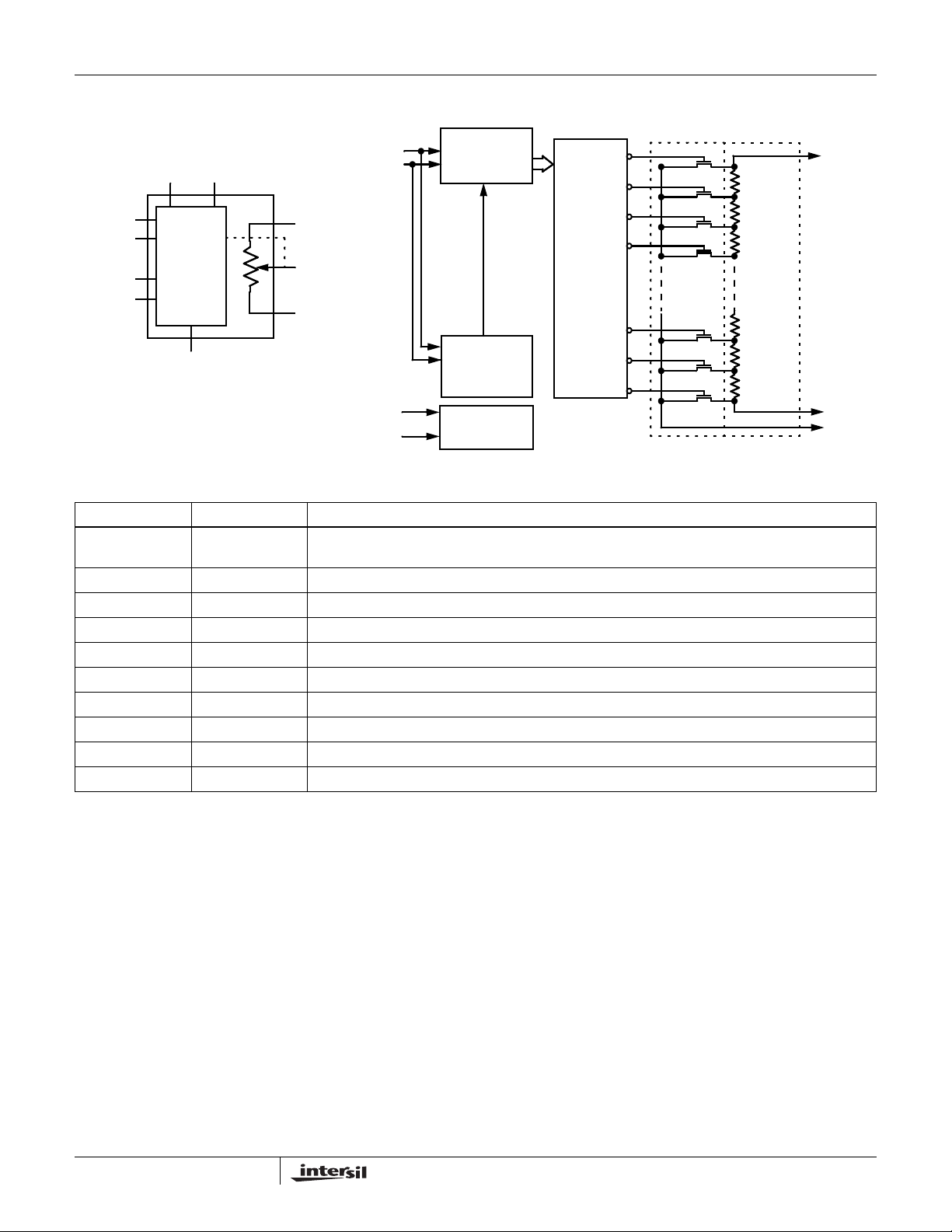
Block Diagram
www.BDTIC.com/Intersil
V
CC
GND
SDA
SCL
ISL23711
7-BIT
WIPER
REGISTER
(VOLATILE)
127
126
R
H
SDA
SCL
INTERFACE
A1
A0
AND
CONTROL
V-
SIMPLE BLOCK DIAGRAM
R
H
R
W
R
L
RECALL
CONTROL
CIRCUITRY
A1
A0
SLAVE
ADDRESS
DECODE
ONE
OF
128
DECODER
DETAILED BLOCK DIAGRAM
Pin Descriptions
PIN NUMBER SYMBOL DESCRIPTION
1 SDA Data I/O for I2C serial interface. It has an open drain output and may be wire ORed with other open
drain active low outputs.
2 V- Negative supply voltage for the potentiometer wiper control.
3 GND Ground. Should be connected to a digital ground
4 A1 A1 and A0 are address select pins used to set the slave address for the I
5 A0 A1 and A0 are address select pins used to set the slave address for the I
6R
7R
8R
9V
H
W
L
CC
10 SCL Clock input for the I
A fixed terminal for one end of the potentiometer resistor.
The wiper terminal which is equivalent to the movable terminal of a potentiometer.
A fixed terminal for one end of the potentiometer resistor.
Positive logic supply voltage.
2
C serial interface.
125
124
TRANSFER
GATES
2
1
0
RESISTOR
ARRAY
2
C serial interface.
2
C serial interface.
R
L
R
W
2
FN6127.0
August 16, 2005
ISL23711
www.BDTIC.com/Intersil
Absolute Maximum Ratings Thermal Information
Temperature under bias . . . . . . . . . . . . . . . . . . . . . .-65°C to +135°C
Storage temperature . . . . . . . . . . . . . . . . . . . . . . . .-65°C to +150°C
Voltage on SDA, SCL, A0, and A1
with Respect to GND . . . . . . . . . . . . . . . . . . . . . -0.3 to V
Voltage on V- (referenced to GND) . . . . . . . . . . . . . . . . . . . . . . . -6V
∆V = |V
(RH)-V(RL)
Lead Temperature (soldering 10s) . . . . . . . . . . . . . . . . . . . . . . 300°C
(10s) . . . . . . . . . . . . . . . . . . . . . . . . . . . . . . . . . . . . . . . . . . ±6mA
I
W
. . . . . . . . . . . . . . . . . . . . . . . . . . . . . . . . . . . . . . . . . -0.3V to 6V
V
CC
, RL, RW . . . . . . . . . . . . . . . . . . . . . . . . . . . . . . . . . . . . V- to V
R
H
ESD Rating (MIL-STD-883, Method 3015.7 . . . . . . . . . . . . . . .>2kV
CAUTION: Stresses above those listed under “Absolute Maximum Ratings” may cause permanent damage to the device. This is a stress rating only; functional
operation of the device (at these or any other conditions above those listed in the operational sections of this specification) is not implied. Exposure to absolute
maximum rating conditions for extended periods may affect device reliability.
NOTE:
3. θ
is measured with the component mounted on a high effective thermal conductivity test board in free air. See Tech Brief TB379 for details.
JA
| . . . . . . . . . . . . . . . . . . . . . . . . . . . . . . . . . . . .12V
CC
+0.3V
CC
Thermal Resistance (Typical, Note 3) θ
MSOP Package . . . . . . . . . . . . . . . . . . . . . . . . . . . . 170
Recommended Operating Conditions
Temperature Range (Industrial) . . . . . . . . . . . . . . . . .-40°C to +85°C
V
. . . . . . . . . . . . . . . . . . . . . . . . . . . . . . . . . . . . . . . . 2.7V to 5.5V
CC
V- . . . . . . . . . . . . . . . . . . . . . . . . . . . . . . . . . . . . . . . . . -2.7V to -5.5V
Analog Specifications Over recommended operating conditions unless otherwise stated.
SYMBOL PARAMETER TEST CONDITIONS MIN
R
TOTAL
V
RH,VRL
R
W
C
H/CL/CW
I
LkgDCP
VOLTAGE DIVIDER MODE (V- @ R
INL
(Note 6)
DNL
(Note 5)
ZSerror
(Note 3)
FSerror
(Note 4)
TC
(Notes 7, 13)
RESISTOR MODE (Measurements between R
RINL
(Note 11)
RDNL
(Note 10)
Roffset
(Note 9)
TC
(Notes 12, 13)
RH to RL Resistance W option 10 kΩ
U option 50 kΩ
to RL Resistance Tolerance -20 +20 %
R
H
RH, RL Terminal Voltage V- V
Wiper Resistance V- = -5.5V; VCC = +5.5V
RW
-V-)/R
CC
CC
unloaded)
TOTAL
Wiper current = (V
Potentiometer Capacitance (Note 13) 10/10/25 pF
Leakage on RH, RL, RW pins Voltage at pins; V- to V
; VCC @ RH; Voltage at RW = V
L
Integral Non-linearity -1 1 LSB
Differential Non-linearity W, U options -0.5 0.5 LSB
Zero-scale Error W option 0 1 4 LSB
U option 0 0.5 2
Full-scale Error W option -4 -1 0 LSB
U option -2 -0.5 0
Ratiometric Temperature Coefficient DCP register set from 16 to 120d, T = -40°C to
V
W
Integral Non-linearity DCP register set between 20 hex and 7F hex.
Differential Non-linearity -0.5 0.5 MI
Offset DCP register set to 00 hex, W option 0 2 5 MI
Resistance Temperature Coefficient DCP register set from 16 to 127d, T = -40°C to
R
+85°C
and RL with RH not connected, or between RW and RH with RL not connected)
Monotonic over all tap positions
DCP register set to 00 hex, U option 0 0.5 2 MI
+85°C
-1 0.1 1 µA
-1 1 MI
TYP
(Note 1) MAX UNIT
70 200 Ω
±4 ppm/°C
±50 ppm/°C
CC
(°C/W)
JA
V
(Note 2)
(Note 2)
(Note 2)
(Note 2)
(Note 8)
(Note 8)
(Note 8)
(Note 8)
3
FN6127.0
August 16, 2005

ISL23711
www.BDTIC.com/Intersil
Operating Specifications Over the recommended operating conditions unless otherwise specified.
SYMBOL PARAMETER TEST CONDITIONS MIN
I
CC1
I
V-
I
SB
I
V-SB
I
LkgDig
t
DCP
(Note 13)
Vpor Power-on Recall for V
SERIAL INTERFACE SPECS
V
V
IH
Hysteresis SDA and SCL Input Buffer Hysteresis 0.05*
V
OL
Cpin
(Note 14)
f
SCL
t
IN
t
AA
t
BUF
t
LOW
t
HIGH
t
SU:STA
t
HD:STA
t
SU:DAT
t
HD:DAT
t
SU:STO
t
HD:STO
VCC Supply Current, Volatile
Write/Read
V- Supply Current, Volatile Write/Read f
VCC Current (Standby) V
f
= 400kHz; SDA = Open; (for I2C, Active,
SCL
Read and Write states only)
= 400kHz; SDA = Open; (for I2C, Active,
SCL
Read and Write states only)
= +5.5V, I2C Interface in Standby State 500 nA
CC
= +3.6V, I2C Interface in Standby State 300 nA
V
CC
V- Current (Standby) V- = -5.5V, I2C Interface in Standby State -500 nA
= -2.7V, I2C Interface in Standby State -300 -1 nA
V-
Leakage Current, at Pins SDA, SCL,
A0, and A1
DCP Wiper Response Time SCL falling edge of last bit of DCP Data Byte to
Voltage at pin from GND to V
CC
wiper change
CC
A0, A1, SDA, and SCL Input Buffer
IL
LOW Voltage
A0, A1, SDA, and SCL Input Buffer
0.7*V
HIGH Voltage
SDA Output Buffer LOW Voltage,
Sinking 4mA
A0, A1, SDA, and SCL Pin
Capacitance
SCL Frequency 400 kHz
Pulse Width Suppression Time at SDA
and SCL Inputs
SCL Falling Edge to SDA Output Data
Val id
Time the Bus Must be Free Before the
Start of a New Transmission
Any pulse narrower than the max spec is
suppressed
SCL falling edge crossing 30% of VCC, until SDA
exits the 30% to 70% of V
window
CC
SDA crossing 70% of VCC during a STOP
condition, to SDA crossing 70% of V
the following START condition
CC
during
Clock LOW Time Measured at the 30% of VCC crossing 1300 ns
Clock HIGH Time Measured at the 70% of VCC crossing 600 ns
START Condition Setup Time SCL rising edge to SDA falling edge. Both
crossing 70% of V
CC
START Condition Hold Time From SDA falling edge crossing 30% of VCC to
SCL falling edge crossing 70% of V
CC
Input Data Setup Time From SDA exiting the 30% to 70% of VCC
window, to SCL rising edge crossing 30% of V
CC
Input Data Hold Time From SCL rising edge crossing 70% of VCC to
SDA entering the 30% to 70% of V
window
CC
STOP Condition Setup Time From SCL rising edge crossing 70% of VCC, to
SDA rising edge crossing 30% of V
CC
STOP Condition Setup Time From SDA rising edge to SCL falling edge. Both
crossing 70% of V
CC
TYP
(Note 1) MAX UNIT
200 µA
-100 -1 µA
-10 10 µA
1µs
2.5 V
-0.3 0.3*V
CC
VCC+
0.3
CC
V
V
V
V
CC
00.4V
10 pF
50 ns
900 ns
1300 ns
600 ns
600 ns
100 ns
0ns
600 ns
600 ns
4
FN6127.0
August 16, 2005

ISL23711
www.BDTIC.com/Intersil
Operating Specifications Over the recommended operating conditions unless otherwise specified. (Continued)
SYMBOL PARAMETER TEST CONDITIONS MIN
t
DH
t
R
(Note 14)
t
F
(Note 14)
Cb
Output Data Hold Time From SCL falling edge crossing 30% of VCC, until
SDA enters the 30% to 70% of V
SDA, SCL, A0, A1 Rise Time From 30% to 70% of V
SDA, SCL, A0, A1 Fall Time From 70% to 30% of V
CC
CC
CC
window
Capacitive Loading of SDA or SCL Total on-chip and off-chip 10 400 pF
0ns
20 +
0.1 * Cb
20 +
0.1 * Cb
(Note 14)
Rpu
(Note 14)
SDA and SCL Bus Pull-up Resistor
Off-chip
Maximum is determined by t
For Cb = 400pF, max is about 2~2.5kΩ
and t
R
F
1kΩ
For Cb = 40pF, max is about 15~20kΩ
t
SU:A
t
HD:A
A0, A1 Setup Time Before START condition 600 ns
A0, A1 Hold Time After STOP condition 600 ns
TYP
(Note 1) MAX UNIT
SDA vs SCL Timing
250 ns
250 ns
SCL
t
SU:STA
SDA
(INPUT TIMING)
SDA
(OUTPUT TIMING)
A0, A1 Pin Timing
SCL
SDA IN
A0, A1
t
HD:ST A
START
t
SU:A
Clk 1
t
HIGH
t
F
t
SU:DAT
t
LOW
t
HD:DAT
t
R
t
SU:STO
t
AA
STOP
t
DH
t
HD:A
t
BUF
5
FN6127.0
August 16, 2005

ISL23711
www.BDTIC.com/Intersil
NOTES:
1. Typical values are for T
2. LSB: [V(RW)
incremental voltage when changing from one tap to an adjacent tap.
3. ZS error = (V(RW)
4. FS error = [V(RW)
5. DNL = [V(RW)
6. INL = V(RW)
7.
TC
V
for i = 16 to 120 decimal, Max( ) is the maximum value of the wiper voltage and Min ( ) is the minimum value of the wiper voltage over the
temperature range.
8. MI =
9. Roffset = R
Roffset = R
10. RDNL = (R
11. RINL = [R
TC
12.
R
for i = 16 to 127, Max( ) is the maximum value of the resistance and Min ( ) is the minimum value of the resistance over the temperature range.
13. This parameter is not 100% tested.
14. These are I
127
– V(RW)
i
– (i • LSB – V(RW)0) for i = 1 to 127.
i
Max V RW()
()Min V RW()
--------------------------------------------------------------- -------------------------------
Max V RW()
()Min V RW()
|R
– R
127
| / 127. R
0
/ MI, when measuring between R
0
/ MI, when measuring between R
127
– R
i
i-1
– (MI • i) – R0] / MI, for i = 16 to 127.
i
Max Ri()Min Ri()–[]
----------------------------------------------------------------
Max Ri()Min Ri()+[]2⁄
2
C specific parameters and are not directly tested, however they are used during device testing to validate device specification.
= 25°C and ±5V supply voltage.
A
– V(RW)0] / 127. V(RW)
– V-) / LSB.
0
– VCC] / LSB.
127
] / LSB-1, for i = 1 to 127. i is the DCP register setting.
i-1
()–
i
()+[]2⁄
i
and R0 are the measured resistances for the DCP register set to 7F hex and 00 hex respectively.
127
) / MI, for i = 16 to 127.
10
---------------- -
×=
125°C
and V(RW)0 are V(RW) for the DCP register set to 7F hex and 00 hex respectively. LSB is the
127
6
10
i
---------------- -
×=
125°C
i
and RL.
W
and RH.
W
6
Test Circuit
TEST POINT
R
W
FORCE
CURRENT
Equivalent Circuit
R
TOTAL
R
H
C
H
C
W
R
W
R
L
C
L
Pin Descriptions
Potentiometer Pins
RH AND R
The high (RH) and low (RL) terminals of the ISL23711 are
equivalent to the fixed terminals of a mechanical
potentiometer. The terminology of R
relative position of the terminal in relation to wiper movement
direction selected by the I
potential on the terminal.
L
and RH references the
L
2
C serial input and not the voltage
R
W
Rw is the wiper terminal and is equivalent to the movable
terminal of a mechanical potentiometer. The position of the
wiper within the array is determined by the control inputs.
BUS INTERFACE PINS
Serial Data Input/Output (SDA)
The SDA is a bidirectional serial data input/output pin for the
2
I
C interface. It receives device address, operation code,
wiper register address and data from an I
2
C external master
device at the rising edge of the serial clock SCL, and it shifts
out data after each falling edge of the serial clock SCL.
SDA requires an external pull-up resistor, since it’s an open
drain output.
Serial Clock (SCL)
This input is the serial clock of the I
2
C serial interface.
Device Address (A1-A0)
The Address inputs are used to set the least significant 2 bits
of the 7-bit I2C interface slave address. A match in the slave
address serial data stream must be made with the Address
input pins in order to initiate communication with the
ISL23711. A maximum of 4 ISL23711 devices may occupy
2
the I
C serial bus.
Principles of Operation
The ISL23711 is an integrated circuit incorporating one DCP
with It’s associated register, and an I
providing direct communication between a host and the
potentiometer and memory. The resistor array is comprised
2
C serial interface
6
FN6127.0
August 16, 2005

ISL23711
www.BDTIC.com/Intersil
of 127 individual resistors connected in series. At either end
of the array and between each resistor is an electronic
switch that transfers the potential at that point to the wiper.
The wiper, when at either fixed terminal, acts like its
mechanical equivalent and does not move beyond the last
position. That is, the counter does not wrap around when
clocked to either extreme.
The electronic switches on the device operate in a “make
before break” mode when the wiper changes tap positions.
DCP Description
The DCP is implemented with a combination of resistor
elements and CMOS switches. The physical ends of the
DCP are equivalent to the fixed terminals of a mechanical
potentiometer (R
intermediate nodes, and is equivalent to the wiper terminal
of a mechanical potentiometer. The position of the wiper
terminal is controlled by a 7-bit volatile Wiper Register (WR).
When the WR contains all zeroes (00h), the wiper terminal
(R
) is closest to its “Low” terminal (RL). When the WR
W
contains all ones (7Fh), the wiper terminal (R
its “High” terminal (R
from all zeroes (0 decimal) to all ones (127 decimal), the
wiper moves monotonically from the position closest to R
the position closest to R
between R
resistance between R
While the ISL23711 is being powered up, the WR is reset to
20h (64 decimal), which locates the R
between R
The WR can be read or written directly using the I2C serial
interface as described in the following sections.
and RL pins). The RW pin is connected to
H
) is closest to
). As the value of the WR increases
H
. At the same time, the resistance
and RL increases monotonically, while the
W
and RH.
L
H
and RW decreases monotonically.
H
W
at the center
W
to
L
indicating START and STOP conditions (See Figure 1). On
power-up of the ISL23711 the SDA pin is in the input mode.
2
All I
C interface operations must begin with a START condition,
which is a HIGH to LOW transition of SDA while SCL is HIGH.
The ISL23711 continuously monitors the SDA and SCL lines for
the START condition and does not respond to any command
until this condition is met (See Figure 1).
2
All I
C interface operations must be terminated by a STOP
condition, which is a LOW to HIGH transition of SDA while
SCL is HIGH (See Figure 1). A STOP condition at the end of
a read operation, or at the end of a write operation to volatile
bytes only places the device in its standby mode.
An ACK, Acknowledge, is a software convention used to
indicate a successful data transfer. The transmitting device,
either master or slave, releases the SDA bus after
transmitting eight bits. During the ninth clock cycle, the
receiver pulls the SDA line LOW to acknowledge the
reception of the eight bits of data (See Figure 2).
The ISL23711 responds with an ACK after recognition of a
START condition followed by a valid Identification Byte, and
once again after successful receipt of an Address Byte. The
ISL23711 also responds with an ACK after receiving a Data
Byte of a write operation. The master must respond with an
ACK after receiving a Data Byte of a read operation
A valid Identification Byte contains 01010 as the five MSBs,
and the following two bits matching the logic values present
at pins A1, and A0. The LSB is in the Read/Write
value is “1” for a Read operation, and “0” for a Write
operation. (See Table 1.)
TABLE 1. IDENTIFICATION BYTE FORMAT
Logic values at pins A1, and A0 respectively
bit. Its
Memory Description
• A read operation to address 0 outputs the value of the
volatile WR.
• A write operation to address 0 only writes to the volatile WR.
I2C Serial Interface
The ISL23711 supports a bidirectional bus oriented protocol.
The protocol defines any device that sends data onto the
bus as a transmitter and the receiving device as the receiver.
The device controlling the transfer is a master and the
device being controlled is the slave. The master always
initiates data transfers and provides the clock for both
transmit and receive operations. Therefore, the ISL23711
operates as a slave device in all applications.
All communication over the I
sending the MSB of each byte of data first.
Protocol Conventions
Data states on the SDA line can change only during SCL LOW
periods. SDA state changes during SCL HIGH are reserved for
2
C interface is conducted by
7
01010A1A0R/W
(MSB) (LSB)
Write Operation
A Write operation requires a START condition, followed by a
valid Identification Byte, a valid Address Byte, a Data Byte,
and a STOP condition. After each of the three bytes, the
ISL23711 responds with an ACK.
Read Operation
A Read operation is initiated by a master using the following
sequence: a START, the Identification byte (slave address)
with the R/W
acknowledge by the ISL23711 (slave device), the mastertransmitter becomes a master receiver and receives the data
byte from the slave-transmitter.The Master receives the data
byte and issues a non-acknowledge (SDA is HIGH), then a
STOP to terminate the read operation. Since the ISL 23711
has just one WR, it will transmit only one byte (see Figure 4).
bit set to “1”. At the moment of the first
August 16, 2005
FN6127.0
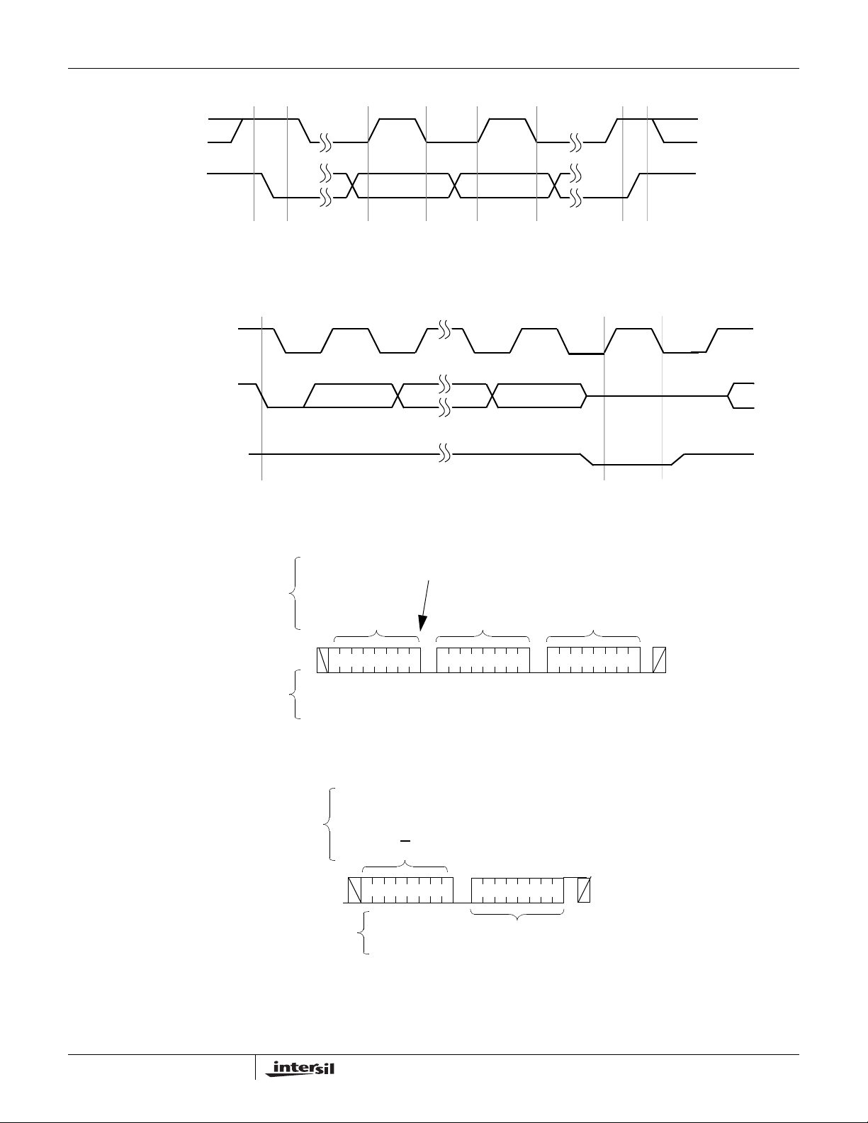
SCL
www.BDTIC.com/Intersil
SDA
ISL23711
SCL FROM
MASTER
SDA OUTPUT FROM
TRANSMITTER
SDA OUTPUT FROM
RECEIVER
SIGNALS FROM
START DATA DATA STOP
STABLE CHANGE
DATA
STABLE
FIGURE 1. VALID DATA CHANGES, START, AND STOP CONDITIONS
81 9
HIGH IMPEDANCE
START ACK
FIGURE 2. ACKNOWLEDGE RESPONSE FROM RECEIVER
WRITE
S
THE MASTER
T
A
IDENTIFICATION
R
T
BYTE
ADDRESS
BYTE
DATA
BYTE
HIGH IMPEDANCE
S
T
O
P
SIGNAL AT SDA
SIGNALS FROM
THE ISL23711
FROM THE
SIGNAL AT SDA
8
00011
FIGURE 3. BYTE WRITE SEQUENCE
SIGNALS
MASTER
SIGNALS FROM
THE SLAVE
000 0
A0A1
0000000
A
C
K
S
T
A
IDENTIFICATION
R
BYTE WITH
T
01011
R/W
=1
A1 A 0
0
A
C
DATA BYTE READ
K
BY MASTER
FIGURE 4. READ SEQUENCE
A
C
K
S
T
O
P
A
C
K
FN6127.0
August 16, 2005
ISL23711
www.BDTIC.com/Intersil
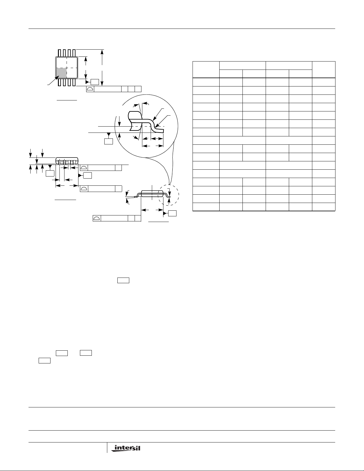
Mini Small Outline Plastic Packages (MSOP)
N
EE1
INDEX
AREA
AA1A2
TOP VIEW
-H-
SIDE VIEW
12
b
e
D
NOTES:
1. These package dimensions are within allowable dimensions of
JEDEC MO-187BA.
2. Dimensioning and tolerancing per ANSI Y14.5M-1994.
3. Dimension “D” does not include mold flash, protrusions or gate
burrs and are measured at Datum Plane. Mold flash, protrusion
and gate burrs shall not exceed 0.15mm (0.006 inch) per side.
4. Dimension “E1” does not include interlead flash or protrusions
and are measured at Datum Plane. Interlead flash and
protrusions shall not exceed 0.15mm (0.006 inch) per side.
5. Formed leads shall be planar with respect to one another within
0.10mm (.004) at seating Plane.
6. “L” is the length of terminal for soldering to a substrate.
7. “N” is the number of terminal positions.
8. Terminal numbers are shown for reference only.
9. Dimension “b” does not include dambar protrusion. Allowable
dambar protrusion shall be 0.08mm (0.003 inch) total in excess
of “b” dimension at maximum material condition. Minimum space
between protrusion and adjacent lead is 0.07mm (0.0027 inch).
- H -
-A -
.
10. Datums and to be determined at Datum plane
11. Controlling dimension: MILLIMETER. Converted inch dimensions are for reference only
-B-
0.20 (0.008) A
GAUGE
PLANE
SEATING
PLANE
0.10 (0.004) C
-A-
0.20 (0.008) C
- B -
0.25
(0.010)
-C-
SEATING
PLANE
a
0.20 (0.008) C
- H -
B
4X θ
C
D
4X θ
L1
C
L
E
1
END VIEW
R1
R
L
C
-B-
M10.118 (JEDEC MO-187BA)
10 LEAD MINI SMALL OUTLINE PLASTIC PACKAGE
INCHES MILLIMETERS
SYMBOL
A 0.037 0.043 0.94 1.10 A1 0.002 0.006 0.05 0.15 A2 0.030 0.037 0.75 0.95 -
b 0.007 0.011 0.18 0.27 9
c 0.004 0.008 0.09 0.20 -
D 0.116 0.120 2.95 3.05 3
E1 0.116 0.120 2.95 3.05 4
e 0.020 BSC 0.50 BSC -
E 0.187 0.199 4.75 5.05 -
L 0.016 0.028 0.40 0.70 6
L1 0.037 REF 0.95 REF -
N10 107
R 0.003 - 0.07 - R1 0.003 - 0.07 - -
o
θ
α
5
o
0
15
o
o
6
o
5
o
0
15
o
o
6
Rev. 0 12/02
NOTESMIN MAX MIN MAX
-
-
All Intersil U.S. products are manufactured, assembled and tested utilizing ISO9000 quality systems.
Intersil Corporation’s quality certifications can be viewed at www.intersil.com/design/quality
Intersil products are sold by description only. Intersil Corporation reserves the right to make changes in circuit design, software and/or specifications at any time without
notice. Accordingly, the reader is cautioned to verify that data sheets are current before placing orders. Information furnished by Intersil is believed to be accurate and
reliable. However, no responsibility is assumed by Intersil or its subsidiaries for its use; nor for any infringements of patents or other rights of third parties which may result
from its use. No license is granted by implication or otherwise under any patent or patent rights of Intersil or its subsidiaries.
For information regarding Intersil Corporation and its products, see www.intersil.com
9
FN6127.0
August 16, 2005
 Loading...