

®
www.BDTIC.com/Intersil
ISL23710
Volatile Digitally Controlled Potentiometer (XDCP™)
Data Sheet August 22, 2005
Terminal Voltage ±3V or ±5V, 128 Taps
Up/Down Interface
The Intersil ISL23710 is a digitally controlled potentiometer
(XDCP). The device consists of a resistor array, wiper
switches, and a control section. The wiper position is
controlled by a Up/Down interface.
The potentiometer is implemented by a resistor array
composed of 127 resistive elements and a wiper switching
network. Between each element and at either end are tap
points accessible to the wiper terminal. The position of the
wiper element is controlled by the CS
, U/D, and INC inputs.
The wiper register is volatile and is reset to midscale on
power up. The wiper position can be locked while powered
up to prevent inadvertent changes.
The device can be used as a three-terminal potentiometer or
as a two-terminal variable resistor in a wide variety of
applications including:
• Industrial and Automotive Control
• Parameter and Bias Adjustments
• Amplifier Bias and Control
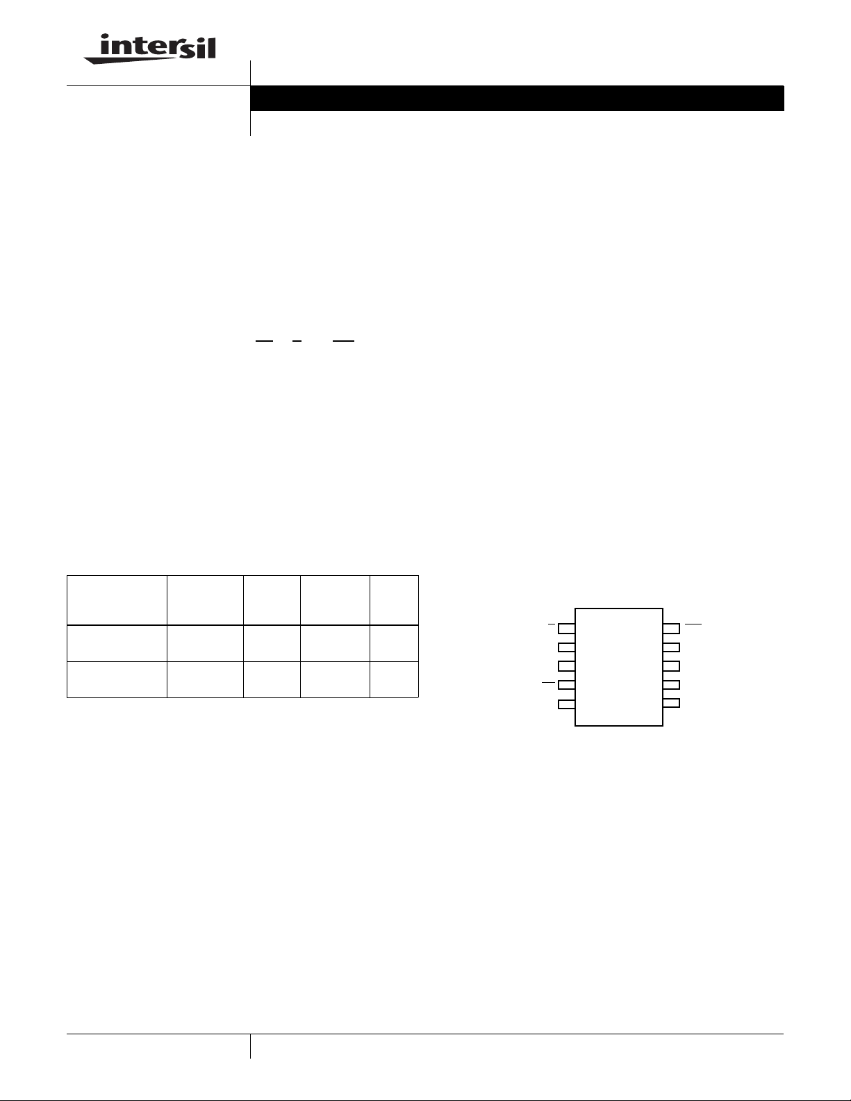
Ordering Information
TEMP
PAR T N UMBER
(BRAND)
ISL23710WIU10Z
(AOG) (Notes 1, 2)
ISL23710UIU10Z
(AOF) (Notes 1, 2)
NOTES:
1. Add “-T” suffix for tape and reel.
2. Intersil Pb-free plus anneal products employ special Pb-free material
sets; molding compounds/die attach materials and 100% matte tin
plate termination finish, which are RoHS compliant and compatible
with both SnPb and Pb-free soldering operations. Intersil Pb-free
products are MSL classified at Pb-free peak reflow temperatures that
meet or exceed the Pb-free requirements of IPC/JEDEC J STD-020.
RESISTANCE
OPTION (Ω)
10K -40 to +85 10 Ld MSOP
50K -40 to +85 10 Ld MSOP
RANGE
(°C) PACKAGE
PKG.
DWG. #
M10.118
(Pb-Free)
M10.118
(Pb-Free)
FN6126.0
Features
• Up/Down Interface with Chip Select Enable
• DCP Terminal Voltage from ±2.7V to ±5V
• 127 Resistive Elements
- Typical R
tempco ±50ppm/°C
TOTAL
- Ratiometric tempco ±4ppm/°C
- End to end resistance range ±20%
- Wiper resistance = 70Ω typ at V
CC
= 3.3V
• Low Power CMOS
- V- = -2.7V to -5.5V
= 2.7V to 5.5V
-V
CC
- Active current, 1mA max
- Standby current, 500nA max
•R
Values = 10kΩ, 50kΩ
TOTAL
• Volatile Wiper Storage with Wiper Locking
• Packages
-10 Ld MSOP
• Pb-Free Plus Anneal Available (RoHS Compliant)
Pinout
ISL23710
(10 LD MSOP)
TOP VIEW
U/D
GND
CS
NC
1
V-
2
3
4
5
INC
10
VCC
9
R
8
L
7
R
W
R
6
H
1
CAUTION: These devices are sensitive to electrostatic discharge; follow proper IC Handling Procedures.
1-888-INTERSIL or 1-888-468-3774
XDCP is a trademark of Intersil, Inc. Copyright Intersil Americas Inc. 2005. All Rights Reserved
| Intersil (and design) is a registered trademark of Intersil Americas Inc.
All other trademarks mentioned are the property of their respective owners.
Block Diagram
www.BDTIC.com/Intersil
ISL23710
UP/DOWN
(U/D
INCREMENT
(INC
DEVICE SELECT
(CS
V
V-
)
INTERFACE
)
)
AND
CONTROL
GND
SIMPLE BLOCK DIAGRAM
CC
U/D
INC
CS
R
H
R
W
R
L
7-BIT
UP/DOWN
COUNTER
RECALL
CONTROL
CIRCUITRY
DECODER
DETAILED BLOCK DIAGRAM
Pin Descriptions
PIN NUMBER SYMBOL DESCRIPTION
1U/D
2 V- Negative supply voltage for the potentiometer wiper control.
3 GND Ground. Should be connected to a digital ground.
4CS
5 NC No Connect. Pin is to be left unconnected.
6R
7R
8R
H
W
L
9 VCC Positive logic supply voltage.
10 INC
Controls the direction of wiper movement and whether the counter is incremented or decremented.
Chip Select. The device is selected when the CS input is LOW.
A fixed terminal for one end of the potentiometer resistor.
The wiper terminal which is equivalent to the movable terminal of a potentiometer.
A fixed terminal for one end of the potentiometer resistor.
Increment input; negative edge triggered.
ONE
OF
128
127
126
125
124
R
H
TRANSFER
GATES
2
1
0
RESISTOR
ARRAY
R
L
R
W
2
FN6126.0
August 22, 2005
ISL23710
www.BDTIC.com/Intersil
Absolute Maximum Ratings Thermal Information
Temperature Under Bias . . . . . . . . . . . . . . . . . . . . .-65°C to +135°C
Storage Temperature . . . . . . . . . . . . . . . . . . . . . . . .-65°C to +150°C
Voltage on CS
with Respect to GND . . . . . . . . . . . . . . . . . . . . -0.3V to VCC+0.3V
Voltage on V- (Referenced to GND) . . . . . . . . . . . . . . . . . . . . . . -6V
∆V = |V
Lead Temperature (Soldering 10s) . . . . . . . . . . . . . . . . . . . . . 300°C
(10s) . . . . . . . . . . . . . . . . . . . . . . . . . . . . . . . . . . . . . . . . . . ±6mA
I
W
. . . . . . . . . . . . . . . . . . . . . . . . . . . . . . . . . . . . . . . . . -0.3V to 6V
V
CC
, RL, RW . . . . . . . . . . . . . . . . . . . . . . . . . . . . . . . . . . . . V- to V
R
H
ESD Rating (MIL-STD-883, Method 3015.7) . . . . . . . . . . . . . . .>2kV
CAUTION: Stresses above those listed under “Absolute Maximum Ratings” may cause permanent damage to the device. This is a stress rating only; functional
operation of the device (at these or any other conditions above those listed in the operational sections of this specification) is not implied. Exposure to absolute
maximum rating conditions for extended periods may affect device reliability.
NOTE:
1. θ
JA
Analog Specifications Over recommended operating conditions unless otherwise stated.
SYMBOL PARAMETER TEST CONDITIONS MIN
R
TOTALRH
V
RH,VRLRH, Rl
R
C
H/CL/CW
I
LkgDCP
VOLTAGE DIVIDER MODE (0V @ RL; V+ @ RH; measured at RW, unloaded)
INL
(Note 6)
DNL
(Note 5)
ZSerror
(Note 3)
FSerror
(Note 4)
TC
(Note 7,13)
RESISTOR MODE (Measurements between RW and RL with RH not connected, or between RW and RH with RL not connected)
RINL
(Note 11)
RDNL
(Note 10)
Roffset
(Note 9)
TC
(Notes 12,13)
, INC, U/D and V
(RH)-V(RL)
is measured with the component mounted on a high effective thermal conductivity test board in free air. See Tech Brief TB379 for details.
W
V
R
| . . . . . . . . . . . . . . . . . . . . . . . . . . . . . . . . . .12V
to RL Resistance W option 10 kΩ
R
to RL Resistance Tolerance -20 +20 %
H
Terminal Voltage V- V
Wiper Resistance V- = -5.5V; VCC = +5.5V,
Potentiometer Capacitance (Note 13) 10/10/
Leakage on DCP Pins Voltage at pin from V- to V
Integral Non-linearity -1 1 LSB
Differential Non-linearity W, U options -0.5 0.5 LSB
Zero-Scale Error W option 0 1 4 LSB
Full-Scale Error W option -4 -1 0 LSB
Ratiometric Temperature Coefficient DCP register set to i = 16 to 120d,
Integral Non-linearity DCP register set between 16 and 127d Monotonic
Differential Non-linearity -0.5 0.5 MI
Offset DCP register set to 0d, W option 0 2 5 MI
Resistance Temperature Coefficient DCP register set to i = 16 to 127d,
CC
CC
U option 50 kΩ
wiper current = (V
U option 0 0.5 2
U option -2 -0.5 0
T = -40°C to 85°C
over all tap positions
DCP register set to 0d, U option 0 0.5 2 MI
T = -40°C to +85°C
Thermal Resistance (Typical, Note 1) θ
MSOP Package . . . . . . . . . . . . . . . . . . . . . . . . . . . . 170
Recommended Operating Conditions
Temperature Range (Industrial). . . . . . . . . . . . . . . . . -40°C to +85°C
V
. . . . . . . . . . . . . . . . . . . . . . . . . . . . . . . . . . . . . . . . 2.7V to 5.5V
CC
V- . . . . . . . . . . . . . . . . . . . . . . . . . . . . . . . . . . . . . . . . . -2.7V to -5.5V
TYP
(Note 1) MAX UNIT
70 200 Ω
- V-)/R
CC
TOTAL
CC
25
-1 0.1 1 µA
±4 ppm/°C
-1 1 MI
±50 ppm/°C
CC
(°C/W)
JA
V
pF
(Note 2)
(Note 2)
(Note 2)
(Note 2)
(Note 8)
(Note 8)
(Note 8)
(Note 8)
3
FN6126.0
August 22, 2005
ISL23710
www.BDTIC.com/Intersil
Operating Specifications Over the recommended operating conditions unless otherwise specified.
SYMBOL PARAMETER TEST CONDITIONS MIN
I
CC1
I
I
SB
I
V-SB
I
LkgDig
Vpor Power-on Recall Voltage Minimum V
SERIAL INTERFACE SPECS
V
V
Hysteresis
(Note 13)
Cpin
(Note 13)
VCC Supply Current, Volatile Write/Read CS = VIL, U/D = VIL or VIH and INC = 0.4V/2.4V
min. t
V- Supply Current, Volatile Write/Read CS = VIL, U/D = VIL or VIH and INC = 0.4V/2.4V
V-
VCC Current (Standby) V
V- Current (Standby) V- = -5.5V, 3 Wire Interface in Standby State -500 nA
Leakage Current, at Pins INC, CS, U/D,
A0, and A1
INC, CS, and U/D Input Buffer LOW
IL
Voltage
INC, CS, and U/D Input Buffer HIGH
IH
Voltage
, CS, and U/D Input Buffer Hysteresis 0.15*
INC
INC
, CS, and U/D Pin Capacitance 10 pF
min. t
CC
V
CC
= -2.7V, 3 Wire Interface in Standby State -300 nA
V-
Voltage at pin from GND to V
, RH, RW not connected
CYC RL
, RH, RW not connected
CYC RL
= +5.5V, 3 Wire Interface in Standby State 500 nA
= +2.7V, 3 Wire Interface in Standby State 300 nA
CC
at which the wiper is Reset 2.5 V
CC
TYP
(Note 1) MAX UNITS
500 µA
-100 µA
-10 10 µA
-0.3 0.3*V
0.7*V
CC
V
CC
CC
VCC+0.3 V
V
V
AC Electrical Specifications V
SYMBOL PARAMETER MIN TYP (Note 1) MAX UNIT
t
Cl
t
lD
t
DI
t
lL
t
lH
t
ICL
(Note 13) INC to RW Change 1 µs
t
IW
t
CYC
t
R, tF
CS to INC Setup 100 ns
INC HIGH to U/D Change 100 ns
U/D to INC Setup 1 µs
INC LOW Period 1 µs
INC HIGH Period 1 µs
Lock Setup Time, INC High to CS High 1 µs
INC Cycle Time 2 µs
INC Input Rise and Fall Time 500 µs
= 5V ±10%, TA = Full Operating Temperature Range unless otherwise stated
CC
4
FN6126.0
August 22, 2005

ISL23710
www.BDTIC.com/Intersil
NOTES:
1. Typical values are for T
2. LSB: [V(RW)
incremental voltage when changing from one tap to an adjacent tap.
3. ZS error = V(RW)
4. FS error = [V(RW)
5. DNL = [V(RW)
6. INL = V(RW)
7.
TC
V
Max( ) is the maximum value of the wiper voltage and Min ( ) is the minimum value of the wiper voltage over the temperature range.
8. MI =
9. Roffset = R
Roffset = R
10. RDNL = (R
11. RINL = [R
12.
TC
R
Max( ) is the maximum value of the resistance and Min ( ) is the minimum value of the resistance over the temperature range.
13. This parameter is not 100% tested.
127
– V(RW)
i
– (i • LSB – V(RW)0) for i = 1 to 127.
i
Max V RW()
()Min V RW()
------------------------------------------------------------- --------------------------------- x
Max V RW()
()Min V RW()
|R
– R
127
0
/MI, when measuring between RW and RL.
0
/MI, when measuring between RW and RH.
127
– R
i
i-1
– (MI • i) – R0]/MI, for i = 16 to 127d.
i
Max Ri()Min Ri()–[]
-------------------------------------------------------------- --
Max Ri()Min Ri()+[]2⁄
= 25°C and 3.3V supply voltage.
A
– V(RW)0]/127. V(RW)
/LSB.
0
– VCC]/LSB.
127
]/LSB-1, for i = 1 to 127. i is the DCP register setting.
i-1
()–
i
()+[]2⁄
i
| /127. R
)/MI, for i = 16 to 127d.
and R0 are the measured resistances for the DCP register set to 7F hex and 00 hex respectively.
127
10
-----------------
×=
125°C
and V(RW)0 are V(RW) for the DCP register set to 7F hex and 00 hex respectively. LSB is the
127
i
i
6
6
10
-----------------=
125°C
Symbol Table
WAVEFORM INPUTS OUTPUTS
Must be steady Will be steady
May change from Low to High Will change from Low to High
May change from High to Low
Don’t Care: Changes Allowed Changing: State Not Known
N/A
Will change from High to Low
Center Line is High Impedance
5
FN6126.0
August 22, 2005

AC Timing
www.BDTIC.com/Intersil
CS
INC
ISL23710
t
CYC
t
CI
t
IL
t
IH
t
ICL
90% 90%
10%
U/D
R
t
ID
t
IW
W
t
DI
(3)
MI
Power Up and Down Requirements
In order to prevent unwanted tap position changes, bring the
CS
and INC high before or concurrently with the VCC pin on
power-up. The potentiometer voltages must be applied after
this sequence is completed. During power-up, the data sheet
parameters for the DCP do not fully apply until 1ms after
V
reaches its final value. The wiper will be set to its initial
CC
value (64d) once V
exceeds V
CC
POR
.
Pin Descriptions
RH and R
The high (RH) and low (RL) terminals of the ISL23710 are
equivalent to the fixed terminals of a mechanical
potentiometer. The terminology of R
relative position of the terminal in relation to wiper movement
direction selected by the U/D
potential on the terminal.
R
W
Rw is the wiper terminal and is equivalent to the movable
terminal of a mechanical potentiometer. The position of the
wiper within the array is determined by the control inputs.
Up/Down (U/D)
The U/D input controls the direction of the wiper movement
and whether the counter is incriminated or decremented.
Increment (INC)
The INC input is negative-edge triggered. Toggling INC will
move the wiper and either increment or decrement the
counter in the direction indicated by the logic level on the
U/D
input.
L
and RH references the
L
input and not the voltage
t
F
t
R
Chip Select (CS)
The device is selected when the CS input is LOW.
Principles of Operation
There are three sections of the ISL23710: the input control,
counter and decode section, and the resistor array. The input
control section operates just like an up/down counter. The
output of this counter is decoded to turn on a single
electronic switch connecting a point on the resistor array to
the wiper output. The resistor array is comprised of 127
individual resistors connected in series. At either end of the
array and between each resistor is an electronic switch that
transfers the potential at that point to the wiper.
The wiper, when at either fixed terminal, acts like its
mechanical equivalent and does not move beyond the last
position. That is, the counter does not wrap around when
clocked to either extreme.
The electronic switches on the device operate in a “make
before break” mode when the wiper changes tap positions. If
the wiper is moved several positions, multiple taps are
connected to the wiper for t
R
value for the device can temporarily be reduced by
TOTAL
(INC to VW change). The
IW
a significant amount if the wiper is moved several positions.
Instructions and Programming
The INC, U/D and CS inputs control the movement of the
wiper along the resistor array. With CS
is selected and enabled to respond to the U/D
inputs. HIGH to LOW transitions on INC
decrement (depending on the state of the U/D
bit counter. The output of this counter is decoded to select
set LOW the device
and INC
will increment or
input) a seven
6
FN6126.0
August 22, 2005
one of one-hundred twenty-eight wiper positions along the
www.BDTIC.com/Intersil
resistive array.
ISL23710
Bringing CS
value to be locked until power down (further changes in CS
and INC will not change the wiper position). Otherwise, INC
should be brought HIGH after CS
changes.
The state of U/D
This allows the host system to enable the device and then
move the wiper up and down until the proper trim is attained.
During initial power-up CS
V
to avoid an accidental tap position change.
CC
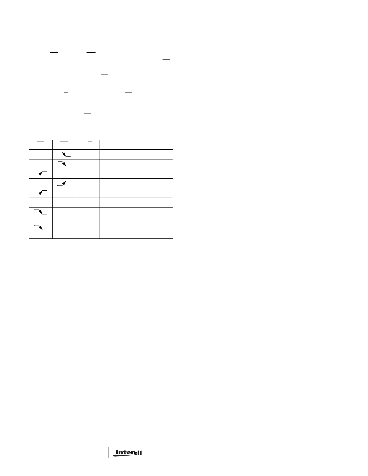
CS INC U/D MODE
L H Wiper Up
L L Wiper Down
H X Standby
H H X Standby
HIGH after INC is HIGH will cause the wiper
to allow continued wiper
may be changed while CS remains LOW.
must go high along with or before
TABLE 1. MODE SELECTION
H X Lock Wiper Value
L X Standby
L H Wiper up One Position
(not recommended)
L L Wiper Down One Position
(not recommended)
7
FN6126.0
August 22, 2005
ISL23710
www.BDTIC.com/Intersil
Mini Small Outline Plastic Packages (MSOP)
N
EE1
INDEX
AREA
AA1A2
-H-
SIDE VIEW
12
TOP VIEW
b
e
D
NOTES:
1. These package dimensions are within allowable dimensions of
JEDEC MO-187BA.
2. Dimensioning and tolerancing per ANSI Y14.5M-1994.
3. Dimension “D” does not include mold flash, protrusions or gate
burrs and are measured at Datum Plane. Mold flash, protrusion
and gate burrs shall not exceed 0.15mm (0.006 inch) per side.
4. Dimension “E1” does not include interlead flash or protrusions
and are measured at Datum Plane. Interlead flash and
protrusions shall not exceed 0.15mm (0.006 inch) per side.
5. Formed leads shall be planar with respect to one another within
0.10mm (.004) at seating Plane.
6. “L” is the length of terminal for soldering to a substrate.
7. “N” is the number of terminal positions.
8. Terminal numbers are shown for reference only.
9. Dimension “b” does not include dambar protrusion. Allowable
dambar protrusion shall be 0.08mm (0.003 inch) total in excess
of “b” dimension at maximum material condition. Minimum space
between protrusion and adjacent lead is 0.07mm (0.0027 inch).
- H -
-A -
.
10. Datums and to be determined at Datum plane
11. Controlling dimension: MILLIMETER. Converted inch dimensions are for reference only
-B-
0.20 (0.008) A
GAUGE
PLANE
SEATING
PLANE
0.10 (0.004) C
-A-
0.20 (0.008) C
- B -
0.25
(0.010)
-C-
SEATING
PLANE
a
0.20 (0.008) C
- H -
B
4X θ
C
D
4X θ
L1
C
C
L
E
1
END VIEW
R1
R
L
-B-
M10.118 (JEDEC MO-187BA)
10 LEAD MINI SMALL OUTLINE PLASTIC PACKAGE
INCHES MILLIMETERS
SYMBOL
A 0.037 0.043 0.94 1.10 A1 0.002 0.006 0.05 0.15 A2 0.030 0.037 0.75 0.95 -
b 0.007 0.011 0.18 0.27 9
c 0.004 0.008 0.09 0.20 -
D 0.116 0.120 2.95 3.05 3
E1 0.116 0.120 2.95 3.05 4
e 0.020 BSC 0.50 BSC -
E 0.187 0.199 4.75 5.05 -
L 0.016 0.028 0.40 0.70 6
L1 0.037 REF 0.95 REF -
N10 107
R 0.003 - 0.07 - R1 0.003 - 0.07 - -
o
θ
α
5
o
0
15
o
o
6
o
5
o
0
15
o
o
6
Rev. 0 12/02
NOTESMIN MAX MIN MAX
-
-
All Intersil U.S. products are manufactured, assembled and tested utilizing ISO9000 quality systems.
Intersil Corporation’s quality certifications can be viewed at www.intersil.com/design/quality
Intersil products are sold by description only. Intersil Corporation reserves the right to make changes in circuit design, software and/or specifications at any time without
notice. Accordingly, the reader is cautioned to verify that data sheets are current before placing orders. Information furnished by Intersil is believed to be accurate and
reliable. However, no responsibility is assumed by Intersil or its subsidiaries for its use; nor for any infringements of patents or other rights of third parties which may result
from its use. No license is granted by implication or otherwise under any patent or patent rights of Intersil or its subsidiaries.
For information regarding Intersil Corporation and its products, see www.intersil.com
8
FN6126.0
August 22, 2005
 Loading...