®
www.BDTIC.com/Intersil
Quad Digitally Controlled Potentiometer (XDCP™)
ISL22449
Data Sheet September 15, 2006
Low Noise, Low Power, SPI® Bus, 128 T aps,
Wiper Only
The ISL22449 integrates four digitally controlled
potentiometers (DCP) and non-volatile memory on a
monolithic CMOS integrated circuit.
The digitally controlled potentiometers are implemented with
a combination of resistor elements and CMOS switches. The
position of the wipers are controlled by the user through the
SPI serial interface. Each potentiometer has an associated
volatile Wiper Register (WR) and a non-volatile Initial Value
Register (IVR) that can be directly written to and read by the
user. The contents of the WR controls the position of the
wiper. At power-up the device recalls the contents of the
DCP’s IVR to the corresponding WR.
The DCP can be used as a voltage divider in a wide variety
of applications including control, parameter adjustments, AC
measurement and signal processing.
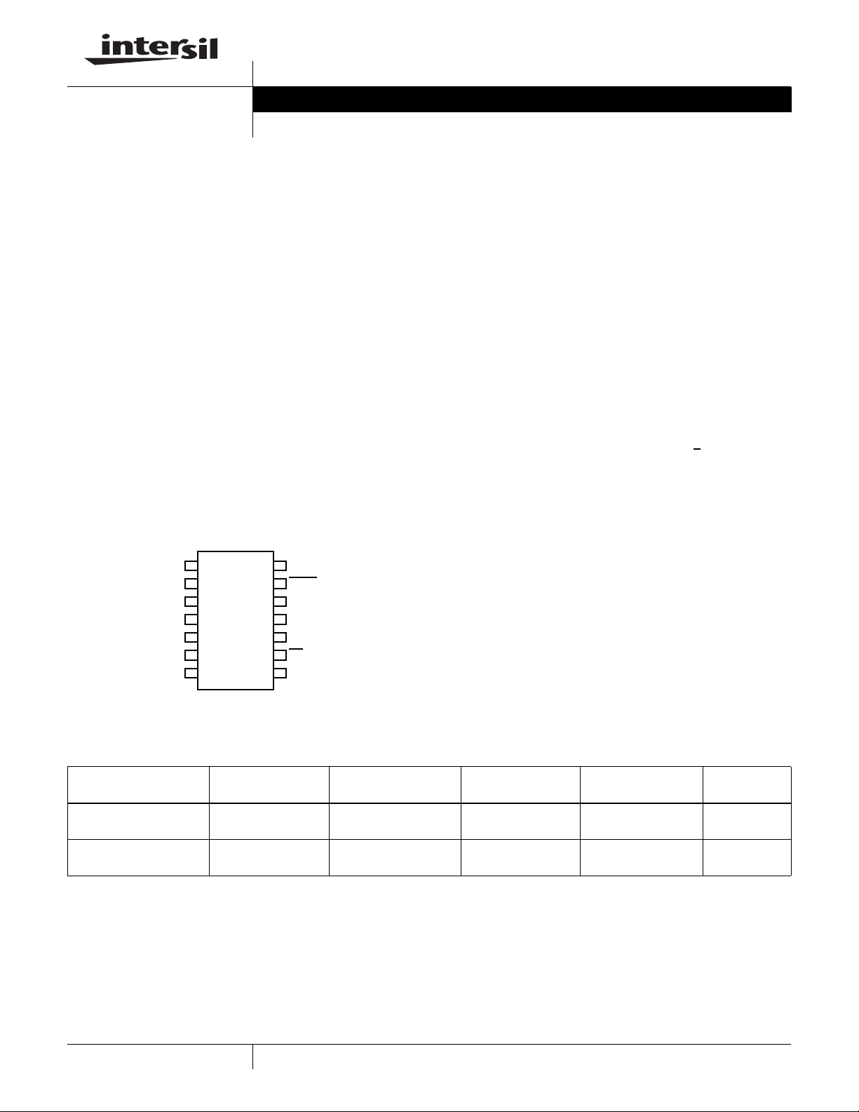
Pinout
ISL22449
(14 LD TSSOP)
TOP VIEW
FN6333.2
Features
• Four potentiometers in one package
• 128 resistor taps
• SPI serial interface
• Non-volatile storage of wiper position
• Wiper resistance: 70Ω typical
• Shutdown mode
• Shutdown current 6.5µA max
• Power supply: 2.7V to 5.5V
•50kΩ or 10kΩ total resistance
• High reliability
- Endurance: 1,000,000 data changes per bit per register
- Register data retention: 50 years @ T <
• 14 Lead TSSOP
• Pb-free plus anneal product (RoHS compliant)
+55°C
RW0
RW3
NC
SCK
SDO
GND
RW2
RW1
1
2
3
4
5
6
7
14
SHDN
13
V
12
CC
NC
11
SDI
10
CS
9
NC
8
Ordering Information
RESISTANCE OPTION
PART NUMBER PART MARKING
ISL22449UFV14Z
(Notes 1, 2)
ISL22449WFV14Z
(Notes 1, 2)
NOTES:
1. Intersil Pb-free plus anneal products employ special Pb-free material sets; molding compounds/die attach materials and 100% matte tin plate
termination finish, which are RoHS compliant and compatible with both SnPb and Pb-free soldering operations. Intersil Pb-free products are
MSL classified at Pb-free peak reflow temperatures that meet or exceed the Pb-free requirements of IPC/JEDEC J STD-020.
2. Add “-TK” suffix for 1,000 Tape and Reel option
22449 UFVZ 50 -40 to +125 14 Ld TSSOP
22449 WFVZ 10 -40 to +125 14 Ld TSSOP
(kΩ)
TEMP. RANGE
(°C) PACKAGE PKG. DWG. #
M14.173
(Pb-free)
M14.173
(Pb-free)
1
1-888-INTERSIL or 1-888-468-3774
CAUTION: These devices are sensitive to electrostatic discharge; follow proper IC Handling Procedures.
| Intersil (and design) and XDCP are registered trademarks of Intersil Americas Inc.
All other trademarks mentioned are the property of their respective owners.
Copyright Intersil Americas Inc. 2006. All Rights Reserved

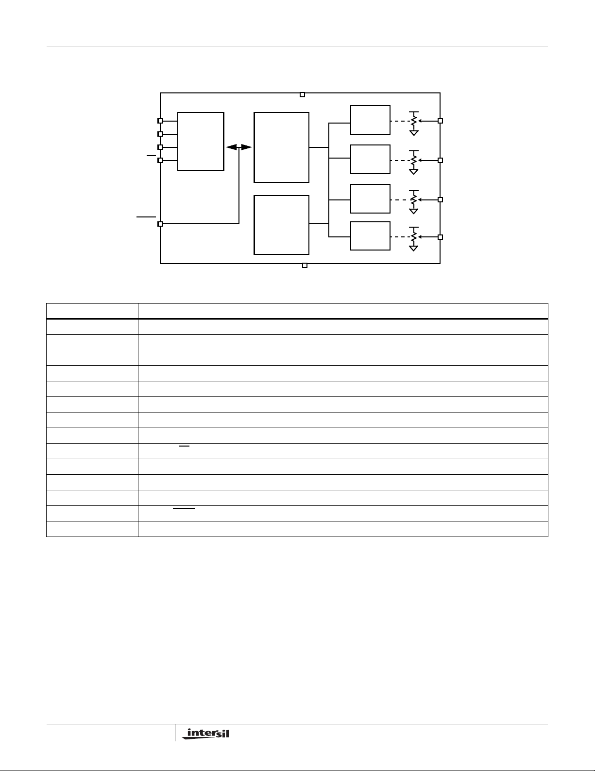
Block Diagram
www.BDTIC.com/Intersil
SCK
SDI
SDO
CS
SPI
INTERFACE
ISL22449
POWER UP
INTERFACE,
CONTROL
AND STA TUS
LOGIC
V
CC
V
CC
WR3
WR2
WR1
V
CC
V
CC
RW3
RW2
RW1
SHDN
NON-
VOLATILE
REGISTERS
GND
Pin Descriptions
TSSOP PIN SYMBOL DESCRIPTION
1 RW3 “Wiper” terminal of DCP3
2NC
3 SCK SPI clock input
4 SDO SPI open drain data output
5 GND Device ground pin and the RL connection for each DCP
6 RW2 “Wiper” terminal of DCP2
7 RW1 “Wiper” terminal of DCP1
8NC
9CS
10 SDI SPI data input
11 NC
12 VCC Power supply pin and the R H connection for each DCP
13 SHDN
14 RW0 “Wiper” terminal of DCP0
SPI Chip Select active low input
Shutdown active low input
WR0
V
CC
RW0
2
FN6333.2
September 15, 2006

ISL22449
www.BDTIC.com/Intersil
Absolute Maximum Ratings Thermal Information
Storage Temperature. . . . . . . . . . . . . . . . . . . . . . . .-65°C to +150°C
Voltage at any Digital Interface Pin
with Respect to GND . . . . . . . . . . . . . . . . . . . . . -0.3V to V
. . . . . . . . . . . . . . . . . . . . . . . . . . . . . . . . . . . . . . . .-0.3V to +6V
V
CC
Voltage at any DCP pin with Respect to GND. . . . . . . -0.3V to V
Lead Temperature (Soldering, 10s) . . . . . . . . . . . . . . . . . . . .+300°C
(10s) . . . . . . . . . . . . . . . . . . . . . . . . . . . . . . . . . . . . . . . . . . ±6mA
I
W
Latchup (Note 4) . . . . . . . . . . . . . . . . . . Class II, Level B @ +125°C
ESD (HBM) . . . . . . . . . . . . . . . . . . . . . . . . . . . . . . . . . . . . . . . 2.5kV
(CDM) . . . . . . . . . . . . . . . . . . . . . . . . . . . . . . . . . . . . . . . . .1kV
CAUTION: Stresses above those listed in “Absolute Maximum Ratings” may cause permanent damage to the device. This is a stress only rating and operation of the
device at these or any other conditions above those indicated in the operational sections of this specification is not implied.
NOTES:
θ
is measured with the component mounted on a high effective thermal conductivity test board in free air. See Tech Brief TB379 for details.
3.
JA
4. Jedec Class II pulse conditions and failure criterion used. Level B exceptions are: using a max positive pulse of 6.5V on the SHDN pin, and using
a max negative pulse of -0.8V for all pins.
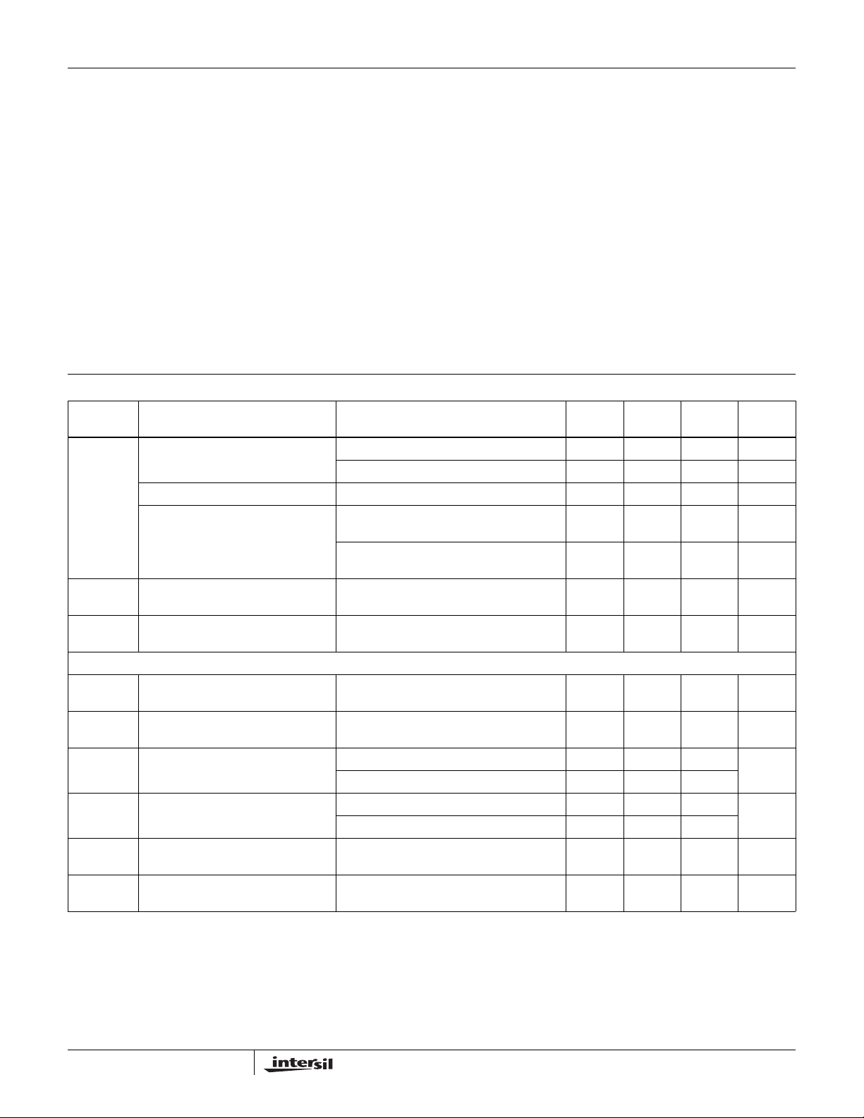
Analog Specifications Over recommended operating conditions unless otherwise stated.
SYMBOL PARAMETER TEST CONDITIONS MIN
R
TOTAL
R
C
(Note 15)
VOLTAGE DIVIDER MODE (measured at R
INL
(Note 10)
DNL
(Note 9)
ZSerror
(Note 7)
FSerror
(Note 8)
V
MATCH
(Note 11)
TC
(Note 12)
End-to-End resistance W option 10 kΩ
U option 50 kΩ
End-to-End resistance tolerance W and U option -20 +20 %
End-to-End Temperature Coefficient W option ±50 ppm/°C
U option ±80 ppm/°C
Wiper resistance VCC = 3.3V @ +25°C,
W
Wiper capacitance
W
Integral non-linearity -1 1 LSB
Differential non-linearity Monotonic over all tap positions -0.5 0.5 LSB
Zero-scale error W option 0 1 5 LSB
Full-scale error W option -5 -1 0 LSB
DCP to DCP matching Any two DCPs at same tap position -2 2 LSB
Ratiometric temperature coefficient DCP register set to 40 hex ±4 ppm/°C
V
W
wiper current = V
i, unloaded; i = 0, 1, 2 or 3)
U option 0 0.5 2
U option -2 -1 0
CC
+0.3
CC
Thermal Resistance (Typical, Note 3) θ
14 Ld TSSOP. . . . . . . . . . . . . . . . . . . . . . . . . . . . . . +100
Maximum Junction Temperature (Plastic Package) . . . . . . . .+150°C
Recommended Operating Conditions
Ambient Temperature . . . . . . . . . . . . . . . . . . . . . . .-40°C to +12 5°C
Voltage for DCP Operation . . . . . . . . . . . . . . . . . . 2.7V to 5.5V
V
CC
Wiper Current . . . . . . . . . . . . . . . . . . . . . . . . . . . . . . . -3mA to 3mA
Power Rating. . . . . . . . . . . . . . . . . . . . . . . . . . . . . . . . . . . . . . .5mW
TYP
(NOTE 5) MAX UNIT
70 200 Ω
CC/RTOTAL
25 pF
(°C/W)
JA
(Note 15)
(Note 15)
(Note 6)
(Note 6)
(Note 6)
(Note 6)
(Note 6)
3
FN6333.2
September 15, 2006

ISL22449
www.BDTIC.com/Intersil
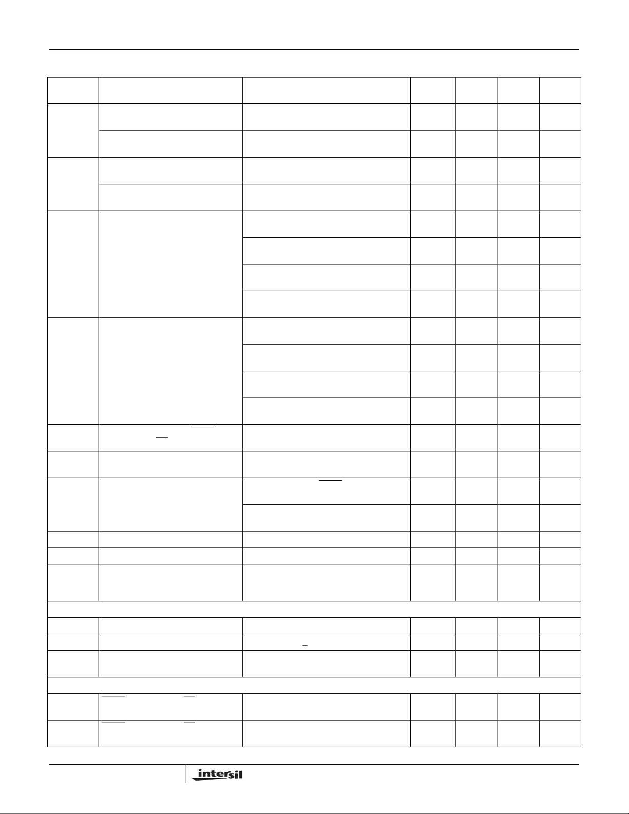
Operating Specifications Over the recommended operating conditions unless otherwise specified.
TYP
SYMBOL PARAMETER TEST CONDITIONS MIN
I
CC1
I
CC2
I
SB
I
SD
I
LkgDig
t
WRT
(Note 15)
t
ShdnRec
(Note 15)
Vpor Power-on recall voltage Minimum V
VccRamp Vcc ramp rate 0.2 V/ms
t
EEPROM SPECIFICATION
t
WC
(Note 13)
SERIAL INTERFACE SPECIFICATIONS
V
V
VCC Supply Current (volatile
write/read)
V
Supply Current (volatile
CC
write/read)
VCC Supply Current ( non-volatile
write/read)
Supply Current ( non-volatile
V
CC
write/read)
VCC Current (standby) V
VCC Current (shutdown) V
Leakage current, at pins SHDN, SCK,
SDI, SDO and CS
DCP wiper response time SCK falling edge of last bit of DCP data byte
DCP recall time from shutdown mode From rising edge of SHDN
Power-up delay VCC above Vpor, to DCP Initial Value
D
EEPROM Endurance 1,000,000 Cycles
EEPROM Retention Temperature
Non-volatile Write cycle time 12 20 ms
SHDN, SCK, SDI, and CS input buffer
IL
LOW voltage
SHDN, SCK, SDI, and CS input buffer
IH
HIGH voltage
V
= +3.6V , 10k DCP , f
CC
active, read and write states)
V
= +3.6V , 50k DCP , f
CC
active, read and write states)
V
= +5.5V , 10k DCP , f
CC
active, read and write states)
V
= +5.5V , 50k DCP , f
CC
active, read and write states)
= +5.5V, 10k DCP, SPI interface in
CC
standby state
= +5.5V, 50k DCP, SPI interface in
V
CC
standby state
= +3.6V, 10k DCP, SPI interface in
V
CC
standby state
V
= +3.6V, 50k DCP, SPI interface in
CC
standby state
= +5.5V @ +85°C, SPI interface in
CC
standby state
V
= +5.5V@ +125°C, SPI interface in
CC
standby state
= +3.6V @ +85°C, SPI interface in
V
CC
standby state
= +3.6V @ +125°C, SPI interface in
V
CC
standby state
Voltage at pin from GND to V
to wiper new position
stored position and RH connection
SCK rising edge of last bit of ACR data byte
to wiper stored position and RH connection
at which memory recall occurs 2.0 2.6 V
CC
Register recall completed, and SPI Interface
in standby state
= 5MHz; (for SPI
SPI
= 5MHz; (for SPI
SPI
= 5MHz; (for SPI
SPI
= 5MHz; (for SPI
SPI
CC
signal to wiper
T < +55°C 50 Years
-0.3 0.3*V
0.7*V
(NOTE 5) MAX UNIT
2.5 mA
0.65 mA
4.0 mA
3.0 mA
2.4 mA
525 µA
1.6 mA
350 µA
5µA
6.5 µA
4µA
5.5 µA
-1 1 µA
1.5 µs
1.5 µs
1.5 µs
3ms
CC
CC
VCC+0.3 V
V
4
FN6333.2
September 15, 2006
 Loading...