®
www.BDTIC.com/Intersil
Quad Digitally Controlled Potentiometers (XDCP™)
ISL22346
Data Sheet February 29, 2008
Low Noise, Low Power I2C® Bus, 128 Taps
The ISL22346 integrates four digitally controlled potentiometers
(DCP) and non-volatile memory on a monolithic CMOS
integrated circuit.
The digitally controlled potentiometers are implemented with
a combination of resistor elements and CMOS switches. The
position of the wipers are controlled by the user through the
2
I
C bus interface. Each potentiometer has an associated
volatile Wiper Register (WR) and a non-volatile Initial Value
Register (IVR) that can be directly written to and read by the
user. The contents of the WR controls the position of the
wiper. At power-up the device recalls the contents of the two
DCP’s IVR to the corresponding WRs.
The DCPs can be used as a three-terminal potentiometers
or as a two-terminal variable resistors in a wide variety of
applications including control, parameter adjustments, and
signal processing.
FN6177.1
Features
• Four potentiometers in one package
• 128 resistor taps
•I2C serial interface
- Three address pins, up to eight devices/bus
• Non-volatile storage of wiper position
• Wiper resistance: 70Ω typical @ V
• Shutdown mode
• Shutdown current 5µA max
• Power supply: 2.7V to 5.5V
•50kΩ or 10kΩ total resistance
• High reliability
- Endurance: 1,000,000 data changes per bit per register
- Register data retention: 50 years @ T <
• 20 Ld TSSOP or 20 Ld TQFN package
• Pb-free (RoHS compliant)
CC
= 3.3V
+55°C
Pinouts
RH3
RL3
RW3
A2
SCL
SDA
GND
RW2
RL2
RH2
ISL22346
(20 LD TSSOP)
TOP VIEW
1
2
3
4
5
6
7
8
9
10
20
19
18
17
16
15
14
13
12
11
RW0
RL0
RH0
SHDN
VCC
A1
A0
RH1
RL1
RW1
RL0
RW0
RH3
RL3
RW3
ISL22346
(20 LD TQFN)
TOP VIEW
RH0
O
20 19
1
2
3
4
5
6
A2
SHDN
7
SCL
VCC
18
8179
SDA
A1
GND
A0
16
RH1
15
RL1
14
13
RW1
RH2
12
RL2
11
10
RW2
Ordering Information
PART NUMBER (Note) PART MARKING RESISTANCE OPTION (kΩ) TEMP. RANGE (°C) PACKAGE (Pb-free) PKG. DWG. #
ISL22346UFV20Z* 22346 UFVZ 50 -40 to +125 20 Ld TSSOP M20.173
ISL22346UFRT20Z* 223 46UFZ 50 -40 to +125 20 Ld 4x4 TQFN L20.4x4A
ISL22346WFV20Z* 22346 WFVZ 10 -40 to +125 20 Ld TSSOP M20.173
ISL22346WFRT20Z* 223 46WFZ 10 -40 to +125 20 Ld 4x4 TQFN L20.4x4A
*Add “-TK” suffix for tape and reel. Please refer to TB347 for details on reel specifications.
NOTE: These Intersil Pb-free plastic packaged products employ special Pb-free material sets; molding compounds/die attach materials and 100%
matte tin plate PLUS ANNEAL - e3 termination finish, which is RoHS compliant and compatible with both SnPb and Pb-free soldering operations.
Intersil Pb-free products are MSL classified at Pb-free peak reflow temperatures that meet or exceed the Pb-free requirements of IPC/JEDEC J
STD-020.
1
1-888-INTERSIL or 1-888-468-3774
CAUTION: These devices are sensitive to electrostatic discharge; follow proper IC Handling Procedures.
| Intersil (and design) and XDCP are registered trademarks of Intersil Americas Inc.
All other trademarks mentioned are the property of their respective owners.
Copyright Intersil Americas Inc. 2006, 2008. All Rights Reserved

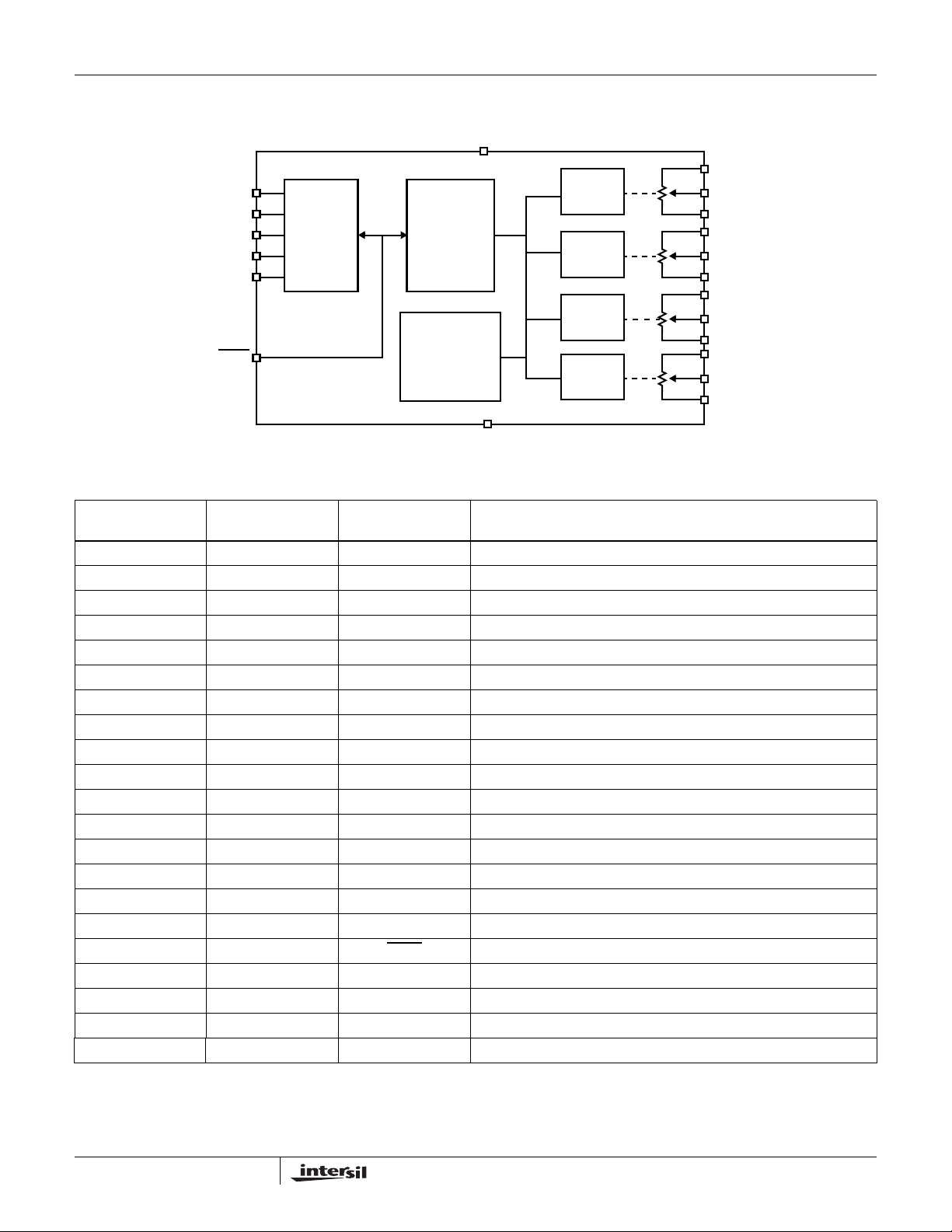
Block Diagram
www.BDTIC.com/Intersil
Pin Descriptions
SCL
SDA
A0
A1
A2
SHDN
I2C
INTERFACE
ISL22346
V
POWER-UP
INTERFACE,
CONTROL
AND STA TUS
LOGIC
NON-
VOLATILE
REGISTERS
CC
GND
WR3
WR2
WR1
WR0
RH3
RW3
RL3
RH2
RW2
RL2
RH1
RW1
RL1
RH0
RW0
RL0
TSSOP PIN
NUMBER
TQFN PIN
NUMBER PIN NAME DESCRIPTION
1 3 RH3 “High” terminal of DCP3
2 4 RL3 “Low” terminal of DCP3
3 5 RW3 “Wiper” terminal of DCP3
2
4 6 A2 Device address input for the I
2
5 7 SCL Open drain I
C interface clock input
C interface
6 8 SDA Open drain Serial data I/O for the I2C interface
7 9 GND Device ground pin
8 10 RW2 “Wiper” terminal of DCP2
9 11 RL2 “Low” terminal of DCP2
10 12 RH2 “High” terminal of DCP2
11 13 RW1 “Wiper” terminal of DCP1
12 14 RL1 “Low” terminal of DCP1
13 15 RH1 “High” terminal of DCP1
2
14 16 A0 Device address input for the I
15 17 A1 Device address input for the I
C interface
2
C interface
16 18 VCC Power supply pin
17 19 SHDN
Shutdown active low input
18 20 RH0 “High” terminal of DCP0
19 1 RL0 “Low” terminal of DCP0
20 2 RW0 “Wiper” terminal of DCP0
EPAD* Exposed Die Pad internally connected to GND
*Note: PCB thermal land for QFN EPAD should be connected to GND plane or left floating. For more information refer to
http://www.intersil.com/data/tb/TB389.pdf
2
FN6177.1
February 29, 2008

ISL22346
www.BDTIC.com/Intersil
Absolute Maximum Ratings Thermal Information
Storage Temperature. . . . . . . . . . . . . . . . . . . . . . . .-65°C to +150°C
Voltage at any Digital Interface Pin
with Respect to GND . . . . . . . . . . . . . . . . . . . . -0.3V to V
. . . . . . . . . . . . . . . . . . . . . . . . . . . . . . . . . . . . . . . .-0.3V to +6V
V
CC
Voltage at any DCP Pin with Respect to GND. . . . . . . -0.3V to V
IW (10s) . . . . . . . . . . . . . . . . . . . . . . . . . . . . . . . . . . . . . . . . . . ±6mA
Latchup (Note 3) . . . . . . . . . . . . . . . . . . Class II, Level B @ +125°C
ESD Ratings
Human Body Model . . . . . . . . . . . . . . . . . . . . . . . . . . . . . . . 2.5kV
Machine Model. . . . . . . . . . . . . . . . . . . . . . . . . . . . . . . . . . . .350V
CAUTION: Do not operate at or near the maximum ratings listed for extended periods of time. Exposure to such conditions may adversely impact product reliability and
result in failures not covered by warranty.
NOTES:
1.
θ
is measured with the component mounted on a high effective thermal conductivity test board in free air. See Tech Brief TB379 for details.
JA
2. For θ
3. Jedec Class II pulse conditions and failure criterion used. Level B exceptions are: using a max positive pulse of 6.5V on the SHDN
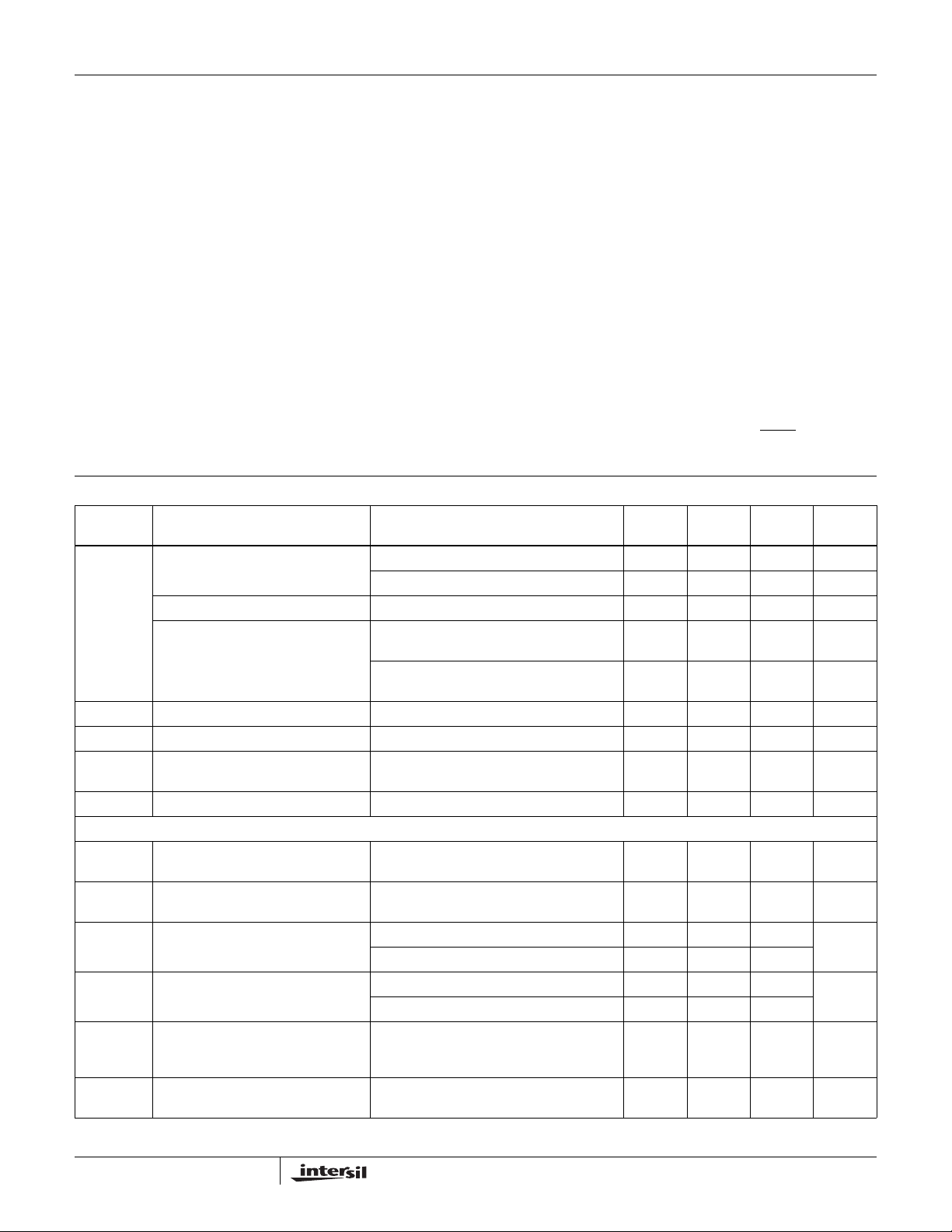
Analog Specifications Over recommended operating conditions, unless otherwise stated.
SYMBOL PARAMETER TEST CONDITIONS
R
V
C
H/CL/CW
(Note 19)
I
VOLTAGE DIVIDER MODE (0V @ R
(Note 9)
(Note 8)
ZSerror
(Note 6)
FSerror
(Note 7)
V
(Note 10)
(Note 11)
, the “case temp” location is the center of the exposed metal pad on the package underside.
JC
a max negative pulse of -0.8V for all pins.
TOTAL
RH
R
LkgDCP
INL
DNL
MATCH
TC
RH to RL Resistance W option 10 kΩ
to RL Resistance Tolerance W and U option -20 +20 %
R
H
End-to-End Temperature Coefficient W option ±50 ppm/°C
, VRLVRH and VRL Terminal Voltages VRH and VRL to GND 0 V
Wiper Resistance VCC = 3.3V, wiper current = VCC/R
W
Potentiometer Capacitance 10/10/25 pF
Leakage on DCP Pins Voltage at pin from GND to V
i; VCC @ RHi; measured at RWi, unloaded; i = 0, 1, 2, or 3)
L
Integral Non-linearity Monotonic over all tap positions -1 1 LSB
Differential Non-linearity Monotonic over all tap positions -0.5 0.5 LSB
Zero-scale Error W option 0 1 5 LSB
Full-scale error W option -5 -1 0 LSB
DCP to DCP Matching Any two DCPs at same tap position, same
Ratiometric Temperature Coefficient DCP register set to 40 hex ±4 ppm/°C
V
+ 0.3
CC
CC
U option 50 kΩ
U option ±80 ppm/°C
U option 0 0.5 2
U option -2 -1 0
voltage at all RH terminals, and same voltage
terminals
at all R
L
Thermal Resistance (Typical, Notes 1, 2) θ
20 Lead TSSOP. . . . . . . . . . . . . . . . . . 95 N/A
20 Lead TQFN . . . . . . . . . . . . . . . . . . 40 3.0
Maximum Junction Temperature (Plastic Package). . . . . . . .+150°C
Pb-free reflow profile . . . . . . . . . . . . . . . . . . . . . . . . . .see link below
http://www.intersil.com/pbfree/Pb-FreeReflow.asp
Recommended Operating Conditions
Temperature Range (Extended Industrial). . . . . . . .-40°C to +125°C
. . . . . . . . . . . . . . . . . . . . . . . . . . . . . . . . . . . . . . . . 2.7V to 5.5V
V
CC
Power Rating. . . . . . . . . . . . . . . . . . . . . . . . . . . . . . . . . . . . . .15mW
Wiper Current . . . . . . . . . . . . . . . . . . . . . . . . . . . . . . . . . . . .±3.0mA
MIN
(Note 20)
TOTAL
CC
-2 2 LSB
TYP
(Note 4)
70 200 Ω
0.1 1 µA
(°C/W) θJC (°C/W)
JA
pin, and using
MAX
(Note 20) UNIT
(Note 17)
(Note 17)
CC
(Note 5)
(Note 5)
(Note 5)
(Note 5)
(Note 5)
V
3
FN6177.1
February 29, 2008

ISL22346
www.BDTIC.com/Intersil
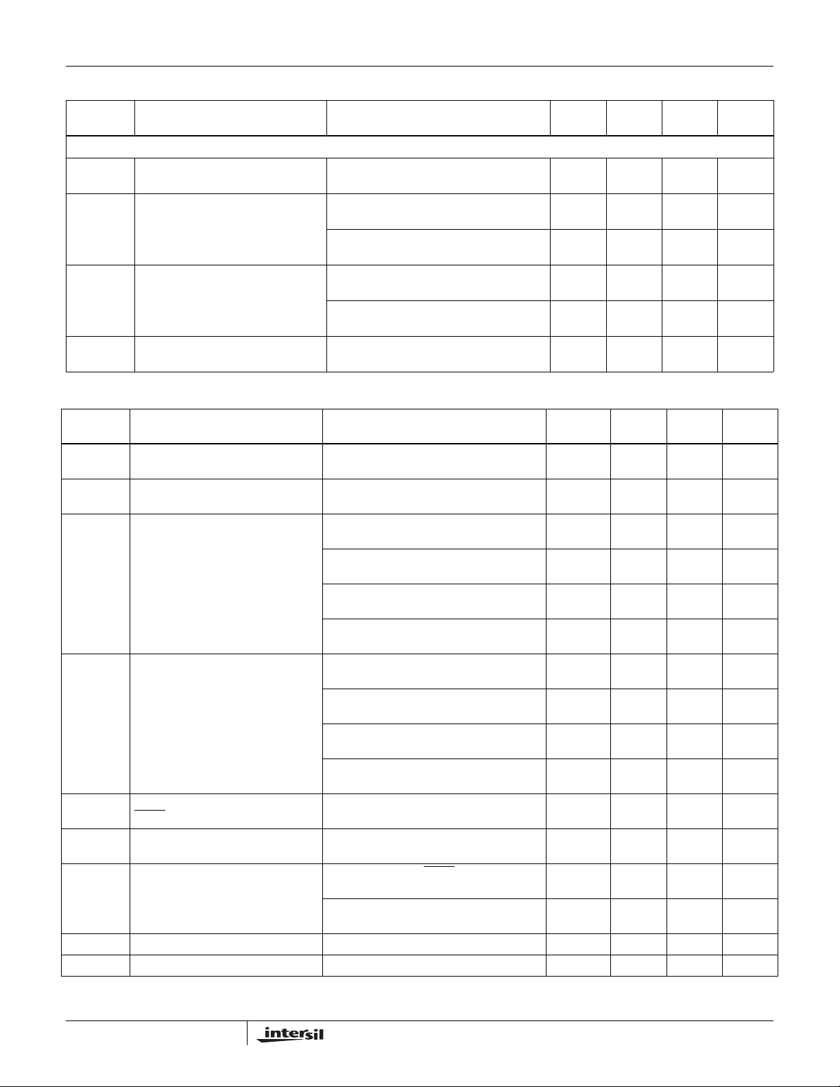
Analog Specifications Over recommended operating conditions, unless otherwise stated. (Continued)
SYMBOL PARAMETER TEST CONDITIONS
RESISTOR MODE (Measurements between RWi and RLi with RHi not connected, or between RWi and RHi with RLi not connected. i = 0, 1, 2 or 3)
RINL
(Note 15)
RDNL
(Note 14)
Roffset
(Note 13)
R
MATCH
(Note 16)
Integral Non-linearity DCP register set between 10h and 7Fh;
Differential Non-linearity DCP register set between 10h and 7Fh;
Offset W option 0 1 5 MI
DCP to DCP Matching Any two DCPs at the same tap position with
monotonic over all tap positions
monotonic over all tap positions, W option
DCP register set between 10h and 7Fh;
monotonic over all tap positions, U option
U option 0 0.5 2 MI
the same terminal voltages
MIN
(Note 20)
-1 1 MI
-1 1 MI
-0.5 0.5 MI
-2 2 MI
Operating Specifications Over the recommended operating conditions, unless otherwise specified.
MIN
SYMBOL PARAMETER TEST CONDITIONS
I
CC1
I
CC2
I
SB
I
SD
I
LkgDig
t
WRT
(Note 19)
t
ShdnRec
(Note 19)
Vpor Power-on Recall Voltage Minimum V
Ramp VCC Ramp Rate 0.2 V/ms
V
CC
VCC Supply Current (Volatile
Write/Read)
VCC Supply Current (Non-volatile
Write/Read)
VCC Current (Standby) V
VCC Current (Shutdown) V
Leakage Current, at Pins A0, A1, A2,
SHDN
, SDA and SCL
DCP Wiper Response Time SCL falling edge of last bit of DCP data byte
DCP Recall Time from Shutdown
Mode
f
= 400kHz; SDA = Open; (for I2C, active,
SCL
read and write states)
f
= 400kHz; SDA = Open; (for I2C, active,
SCL
read and write states)
= +5.5V @ +85°C, I2C interface in
CC
standby state
= +5.5V @ +125°C, I2C interface in
V
CC
standby state
= +3.6V @ +85°C, I2C interface in
V
CC
standby state
= +3.6V @ +125°C, I2C interface in
V
CC
standby state
= +5.5V @ +85°C, I2C interface in
CC
standby state
= +5.5V @ +125°C, I2C interface in
V
CC
standby state
= +3.6V @ +85°C, I2C interface in
V
CC
standby state
= +3.6V @ +125°C, I2C interface in
V
CC
standby state
Voltage at pin from GND to V
to wiper new position
From rising edge of SHDN
stored position and RH connection
SCL falling edge of last bit of ACR data byte
to wiper stored position and RH connection
at which memory recall occurs 2.0 2.6 V
CC
CC
signal to wiper
(Note 20)
-1 1 µA
TYP
(Note 4)
TYP
(Note 4)
1.5 µs
1.5 µs
1.5 µs
MAX
(Note 20) UNIT
MAX
(Note 20) UNIT
0.5 mA
3mA
5µA
7µA
3µA
5µA
3µA
5µA
2µA
4µA
(Note 12)
(Note 12)
(Note 12)
(Note 12)
(Note 12)
(Note 12)
4
FN6177.1
February 29, 2008

ISL22346
www.BDTIC.com/Intersil
Operating Specifications Over the recommended operating conditions, unless otherwise specified. (Continued)
SYMBOL PARAMETER TEST CONDITIONS
t
Power-up Delay VCC above Vpor, to DCP Initial Value
D
Register recall completed, and I
in standby state
EEPROM SPECIFICATION
EEPROM Endurance 1,000,000 Cycles
+55°C 50 Years
t
WC
EEPROM Retention Temperature T <
Non-volatile Write Cycle Time 12 20 ms
(Note 18)
SERIAL INTERFACE SPECIFICATIONS
V
V
Hysteresis
V
OL
Cpin
(Note 19)
f
SCL
t
sp
t
AA
t
BUF
A2, A1, A0, SHDN, SDA, and SCL
IL
Input Buffer LOW Voltage
A2, A1, A0, SHDN, SDA, and SCL
IH
Input Buffer HIGH Voltage
SDA and SCL Input Buffer Hysteresis 0.05*V
SDA Output Buffer LOW Voltage,
Sinking 4mA
A2, A1, A0, SHDN
, SDA, and SCL Pin
Capacitance
SCL Frequency 400 kHz
Pulse Width Suppression Time at SDA
and SCL Inputs
SCL Falling Edge to SDA Output Data
Valid
Time the Bus Must be Free Before the
Start of a New Transmission
Any pulse narrower than the max spec is
suppressed
SCL falling edge crossing 30% of VCC, until
SDA exits the 30% to 70% of V
SDA crossing 70% of VCC during a STOP
condition, to SDA crossing 70% of V
during the following START condition
t
LOW
t
HIGH
t
SU:STA
t
HD:STA
t
SU:DAT
t
HD:DAT
Clock LOW Time Measured at the 30% of VCC crossing 1300 ns
Clock HIGH Time Measured at the 70% of VCC crossing 600 ns
START Condition Setup Time SCL rising edge to SDA falling edge; both
crossing 70% of V
CC
STAR T Condition Hold Time From SDA falling edge crossing 30% of VCC
to SCL falling edge crossing 70% of V
Input Data Setup Time From SDA exiting the 30% to 70% of VCC
window, to SCL rising edge crossing 30% of
V
CC
Input Data Hold Time From SCL rising edge crossing 70% of VCC
to SDA entering the 30% to 70% of V
window
t
SU:STO
STOP Condition Setup Time From SCL rising edge crossing 70% of VCC,
to SDA rising edge crossing 30% of V
t
HD:STO
t
DH
STOP Condition Hold Time for Read,
or Volatile Only Write
Output Data Hold Time From SCL falling edge crossing 30% of VCC,
From SDA rising edge to SCL falling edge;
both crossing 70% of V
CC
until SDA enters the 30% to 70% of V
window
t
t
SDA and SCL Rise Time From 30% to 70% of V
R
SDA and SCL Fall Time From 70% to 30% of V
F
CC
CC
2
C Interface
window
CC
CC
CC
CC
CC
CC
MIN
(Note 20)
-0.3 0.3*V
0.7*V
CC
00.4V
1300 ns
600 ns
600 ns
100 ns
0ns
600 ns
1300 ns
0ns
20 +
0.1*Cb
20 +
0.1*Cb
TYP
(Note 4)
CC
10 pF
MAX
(Note 20) UNIT
3ms
V
V
+ 0.3 V
CC
CC
V
50 ns
900 ns
250 ns
250 ns
5
FN6177.1
February 29, 2008
 Loading...