

®
www.BDTIC.com/Intersil
Dual Digitally Controlled Potentiometers (XDCP™)
ISL22326WMVEP
Data Sheet December 17, 2007
Low Noise, Low Power, I2C® Bus, 128 T a ps
The ISL22326WMVEP integrates two digitally controlled
potentiometers (XDCP) and non-volatile memory on a
monolithic CMOS integrated circuit.
The digitally controlled potentiometers are implemented with
a combination of resistor elements and CMOS switches. The
position of the wipers are controlled by the user through the
2
I
C bus interface. Each potentiometer has an associated
volatile Wiper Register (WR) and a non-volatile Initial Value
Register (IVR) that can be directly written to and read by the
user. The contents of the WR controls the position of the
wiper . At power-up, the device reca lls the content s of the two
DCP’s IVR to the corresponding WRs.
The DCPs can be used as three-terminal potentiometers or
as two-terminal variable resistors in a wide variety of
applications including control, parameter adjustments and
signal processing.
Device Information
The specifications for an Enhanced Product (EP) device are
defined in a Vendor Item Drawing (VID), which is controlled
by the Defense Supply Center in Columbus (DSCC).
“Hot-links” to the applicable VID and other supporting
application information are provided on our website.
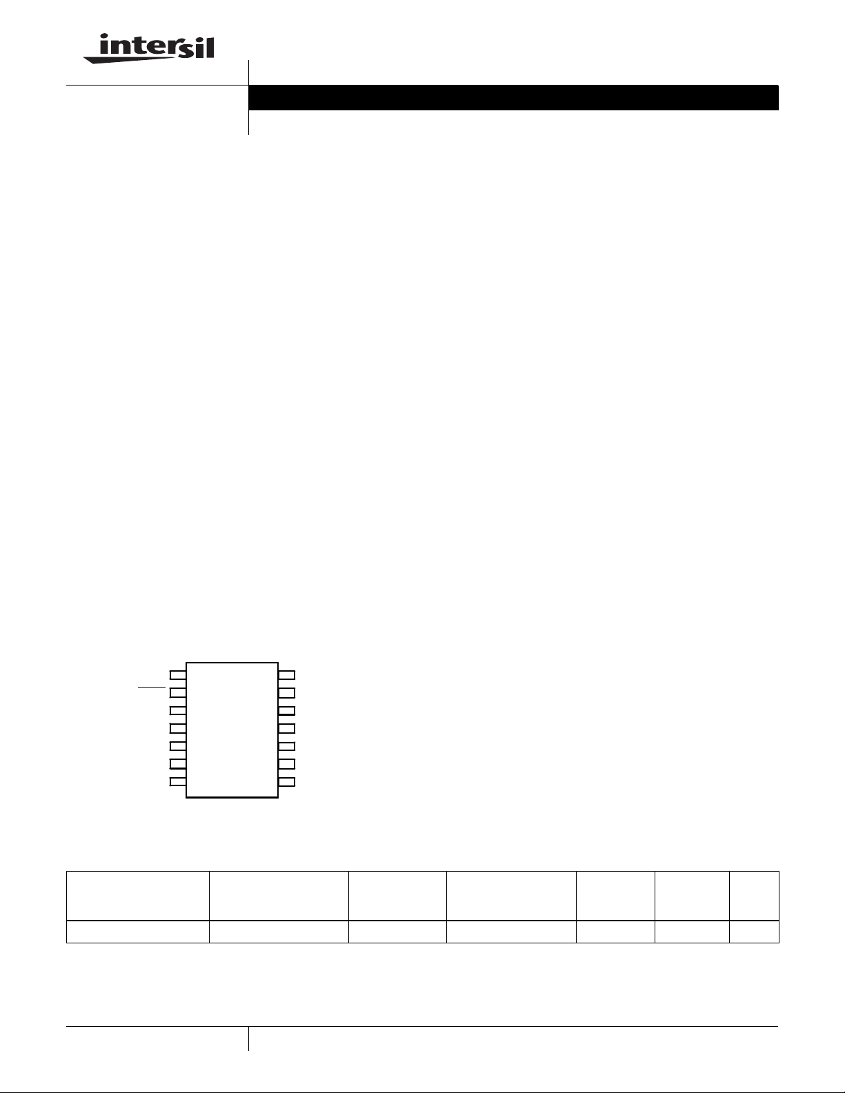
Pinout
ISL22326WMVEP
(14 LD TSSOP)
TOP VIEW
V
CC
SHDN
RH0
RL0
RW0
A2
SCL
1
2
3
4
5
6
7
14
A1
13
A0
RH1
12
11
RL1
RW1
10
9
GND
SDA
8
FN6623.0
Features
• Specifications per DSCC VID V62/08604-01XE
• Full Mil-Temp Electrical Performance from -55°C to +125°C
• Controlled Baseline with One Wafer Fabrication Site and
One Assembly/Test Site
• Full Homogeneous Lot Processing in Wafer Fab
• No Combination of Wafer Fabrication Lots in Assembly
• Full Traceability Through Assembly and Test by
Date/Trace Code Assignment
• Enhanced Process Change Notification
• Enhanced Obsolescence Management
• Eliminates Need for Up-Screening a COTS Component
• Two Potentiometers in One Package
• 128 Resistor Taps
2
C Serial Interface
•I
- Three Address Pins, Up To Eight Devices/Bus
• Non-volatile Storage of Wiper Position
• Wiper Resistance: 70Ω Typical @ 3.3V
• Shutdown Mode
• Shutdown Current 5µA Max
• Power Supply: 2.7V to 5.5V
•10kΩ Total Resistance
• High Reliability
- Endurance: 1,000,000 Data Changes Per Bit Per
Register
- Register Data Retention:
- 10 years @ T ≤ +125°C
- 15 years @ T ≤ +90°C
- 50 years @ T ≤ +55°C
• 14 Ld TSSOP
Ordering Information
VENDOR PART NUMBER
(Notes 1, 2) VENDOR ITEM DRAWING PART MARKING
ISL22326WMVEP V62/08604-01XE 22326 WMVEP 10 -55 to +125 14 Ld TSSOP M14.173
NOTES:
1. Add “-TK” suffix for tape and reel. Please refer to TB347 for details on reel specifications.
2. Devices must be procured to the VENDOR PART NUMBER.
1
1-888-INTERSIL or 1-888-468-3774
CAUTION: These devices are sensitive to electrostatic discharge; follow proper IC Handling Procedures.
RESISTANCE OPTION
(kΩ)
| Intersil (and design) and XDCP are registered trademarks of Intersil Americas Inc.
All other trademarks mentioned are the property of their respective owners.
TEMP.
RANGE
(°C) PACKAGE
Copyright Intersil Americas Inc. 2007. All Rights Reserved
PKG.
DWG. #
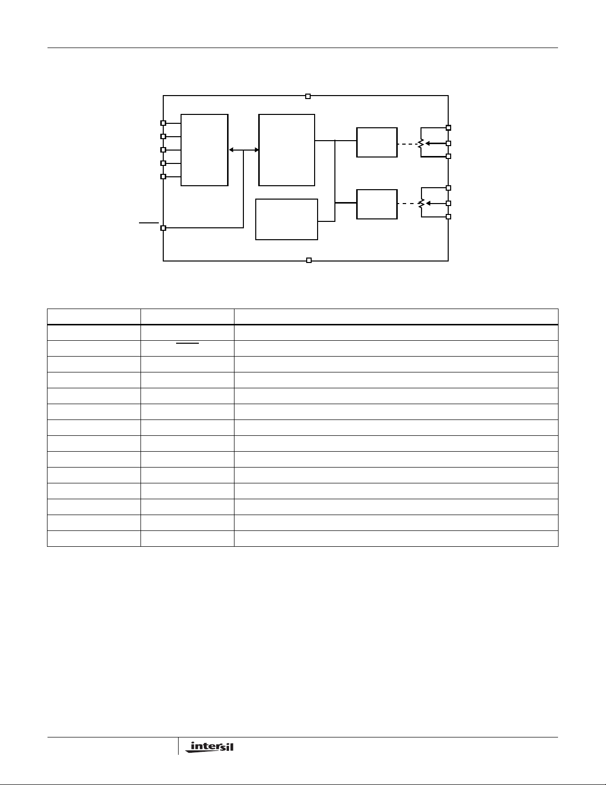
Block Diagram
www.BDTIC.com/Intersil
ISL22326WMVEP
V
CC
SCL
SDA
A0
A1
A2
SHDN
I2C
INTERFACE
POWER-UP
INTERFACE,
CONTROL
AND STA TUS
LOGIC
NON-
VOLATILE
REGISTERS
GND
Pin Descriptions
TSSOP PIN SYMBOL DESCRIPTION
1V
2SHDNShutdown active low input
3 RH0 “High” terminal of DCP0
4 RL0 “Low” terminal of DCP0
5 RW0 “Wiper” terminal of DCP0
6 A2 Device address input for the I
7 SCL Open drain I
8 SDA Open drain Serial data I/O for the I2C interface
9 GND Device ground pin
10 RW1 “Wiper” terminal of DCP1
11 RL1 “Low” terminal of DCP1
12 RH1 “High” terminal of DCP1
13 A0 Device address input for the I
14 A1 Device address input for the I
CC
Power supply pin
2
C interface clock input
2
C interface
2
C interface
2
C interface
WR1
WR0
RH1
RW1
RL1
RH0
RW0
RL0
2
FN6623.0
December 17, 2007

ISL22326WMVEP
www.BDTIC.com/Intersil
Thin Shrink Small Outline Plastic Packages (TSSOP)
N
INDEX
AREA
123
0.05(0.002)
-AD
e
b
0.10(0.004) C AM BS
NOTES:
1. These package dimensions are within allowable dimensions of
JEDEC MO-153-AC, Issue E.
2. Dimensioning and tolerancing per ANSI Y14.5M-1982.
3. Dimension “D” does not include mold flash, protrusions or gate burrs.
Mold flash, protrusion and gate burrs shall not exceed 0.15mm
(0.006 inch) per side.
4. Dimension “E1” does not include interlead flash or protrusions. Interlead flash and protrusions shall not exceed 0.15mm (0.006 inch) per
side.
5. The chamfer on the body is optional. If it is not present, a visual index
feature must be located within the crosshatched area.
6. “L” is the length of terminal for soldering to a substrate.
7. “N” is the number of terminal positions.
8. Terminal numbers are shown for reference only.
9. Dimension “b” does not include dambar protrusion. Allowable dambar
protrusion shall be 0.08mm (0.003 inch) total in excess of “b” dimension at maximum material condition. Minimum space between protrusion and adjacent lead is 0.07mm (0.0027 inch).
10. Controlling dimension: MILLIMETER. Converted inch dimensions
are not necessarily exact. (Angles in degrees)
E1
-B-
SEATING PLANE
A
-C-
M
0.25(0.010) BM M
E
α
A1
0.10(0.004)
GAUGE
PLANE
0.25
0.010
A2
L
c
M14.173
14 LEAD THIN SHRINK SMALL OUTLINE PLASTIC
PACKAGE
INCHES MILLIMETERS
SYMBOL
A - 0.047 - 1.20 -
A1 0.002 0.006 0.05 0.15 -
A2 0.031 0.041 0.80 1.05 -
b 0.0075 0.0118 0.19 0.30 9
c 0.0035 0.0079 0.09 0.20 -
D 0.195 0.199 4.95 5.05 3
E1 0.169 0.177 4.30 4.50 4
e 0.026 BSC 0.65 BSC -
E 0.246 0.256 6.25 6.50 -
L 0.0177 0.0295 0.45 0.75 6
N14 147
o
α
0
o
8
o
0
o
8
NOTESMIN MAX MIN MAX
-
Rev. 2 4/06
All Intersil U.S. products are manufactured, assembled and tested utilizing ISO9000 quality systems.
Intersil Corporation’s quality certifications can be viewed at www.intersil.com/design/quality
Intersil products are sold by description only. Intersil Corporation reserves the right to make changes in circuit design, software and/or specifications at any time without
notice. Accordingly, the reader is cautioned to verify that data sheets are current before placing orders. Information furnished by Intersil is believed to be accurate and
reliable. However, no responsibility is assumed by Intersil or its subsidiaries for its use; nor for any infringements of patents or other rights of third parties which may result
from its use. No license is granted by implic atio n or other wise u nde r any p a tent or patent rights of Intersil or its subsidiaries.
For information regarding Intersil Corporation and its products, see www.intersil.com
3
FN6623.0
December 17, 2007
 Loading...