

®
ISL21400
Data Sheet April 24, 2007
Programmable Temperature Slope
Voltage Reference
The ISL21400 features a precision voltage reference
combined with a temperature sensor whose output voltage
varies linearly with temperature. The precision 1.20V
reference has a very low temperature coefficient (tempco),
and its output voltage is scaled by an internal DAC (V
REF
) to
produce a temperature stable output voltage that is
programmable from 0V to 1.20V. The output voltage from the
temperature sensor (V
) is summed with V
TS
to produce
REF
a temperature dependent output voltage.
The slope of the V
portion of the output voltage can be
TS
programmed to be positive or negative in the range
-2.1mV/°C to +2.1mV/°C. A programmable gain amplifier
(PGA) sums the V
and the V
TS
voltages and provides
REF
gains of 1x, 2x, and 4x to scale the output up to 4.8V and the
slope to ±8.4mV/°C.
The V
resolution via an I
non-volatile registers. The PGA gain is also set via the I
REF
and V
terms are programmable with 8 bits of
TS
2
C bus and the values are stored in
2
C
bus and the value is stored in a non-volatile register.
Non-volatile memory storage assures the programmed
settings are retained on power-down, eliminating the need
for software initialization at device power-up.
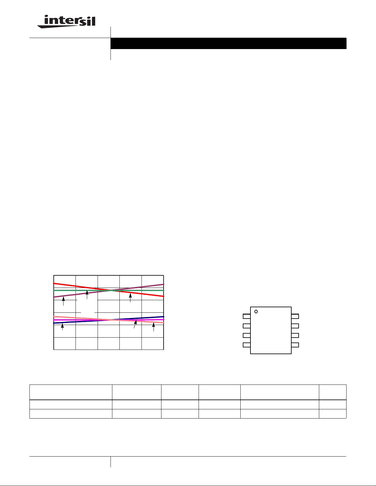
Temperature Characteristics Curve
3.0
2.5
2.0
TS = 0
1.5
VREF (V)
1.0
TS = 0
0.5
0.0
-40 -15 10 35 60 85
AV = 2
TS = 127
= 1
A
V
TEMPERATURE (°C)
TS = 255
TS = 255
TS = 127
FN8091.1
Features
• Programmable reference voltage
• Programmable temperature slope
• Programmable Gain Amplifier
• Non-volatile storage of programming registers
•I2C serial interface
• 2% total accuracy over temperature and V
CC
range
• 200µA typical active supply current
• Operating temperature range = -40°C to +85°C
• 8 Ld MSOP package
• Pb-free plus anneal available (RoHS compliant)
Applications
• RF power amplifier bias compensation
• LCD bias compensation
• Laser diode bias compensation
• Sensor bias and linearization
• Data acquisition systems
• Variable DAC reference
• Amplifier biasing
Pinout
ISL21400
(8 LD MSOP)
TOP VIEW
A2
V
A1
A0
SS
1
2
3
4
V
CC
8
V
7
OUT
6
SDA
SCL
5
Ordering Information
RANGE
V
DD
PART NUMBER (Note) PART MARKING
ISL21400IU8Z DEW 2.7 to 5.5 -40 to +85 8 Ld MSOP (3.0mm), green mtl M8.118
ISL21400IU8Z-TK DEW 2.7 to 5.5 -40 to +85 8 Ld MSOP (3.0mm), green mtl M8.118
NOTE: Intersil Pb-free products employ special Pb-free ma terial sets; molding compou nds/die att ach materials an d 100% matte tin plate termination
finish, which are RoHS compliant and compatible with both SnPb and Pb-free soldering operations. Intersil Pb-free products are MSL classified at
Pb-free peak reflow temperatures that meet or exceed the Pb-free requirements of IPC/JEDEC J STD-020.
1
(V)
CAUTION: These devices are sensitive to electrostatic discharge; follow proper IC Handling Procedures.
1-888-INTERSIL or 1-888-468-3774
TEMP RANGE
(°C)
| Intersil (and design) is a registered trademark of Intersil Americas Inc.
Copyright Intersil Americas Inc. 2006, 2007. All Rights Reserved
All other trademarks mentioned are the property of their respective owners.
PACKAGE
(Pb-free)
PKG.
DWG. #
ISL21400
Pin Description
MSOP SYMBOL DESCRIPTION
1 A2 Hardwire slave address pin for I
2 A1 Hardwire slave address pin for I
3 A0 Hardwire slave address pin for I
4V
SS
Ground pin
2
C serial bus
2
C serial bus
2
C serial bus
5 SCL Serial bus clock input
6 SDA Serial bus data input/output
7 VOUT Output voltage
8V
CC
Device power supply
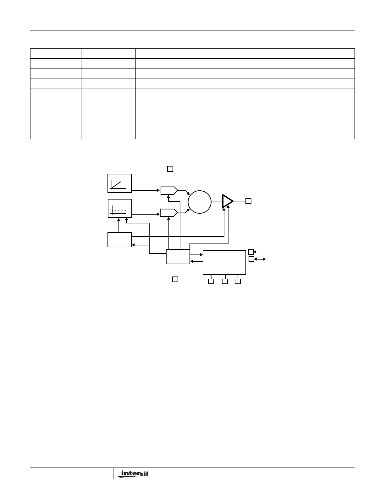
Block Diagram
VCC
TEMP
SENSE
V
BIAS
n = 0 to 255
m = 0 to 255
REF
V
V
REF
(n)
TS
DAC
(m)
DAC
EEPROM
5 BYTES
VSS
S
COMMUNICATIONS
A
AND
REGISTERS
A0 A1 A2
GAIN
SELECT
AV = 1, 2, 4
V
OUT
SCL
SDA
2
FN8091.1
April 24, 2007
ISL21400
Absolute Maximum Ratings Thermal Information
Supply Voltage Range. . . . . . . . . . . . . . . . . . . . . . . . . . .-1V to 6.5V
Storage Temperature Range . . . . . . . . . . . . . . . . . .-65°C to +150°C
Voltage on V
Pin . . . . . . . . . . . . . . . . . . . . . . . . . . . . .0V to V
OUT
CC
Voltage on All Other Pins . . . . . . . . . . . . . . . . . .-0.3V to VCC+0.3V
Lead Temperature (Soldering, 10s) . . . . . . . . . . . . . . . . . . . .+300°C
ESD Rating
Human Body Model . . . . . . . . . . . . . . . . . . . . . . . . . . . . . . . . .2kV
Machine Model. . . . . . . . . . . . . . . . . . . . . . . . . . . . . . . . . . . 200V
CAUTION: Stresses above those listed in “Absolute Maximum Ratings” may cause permanent damage to the device. This is a stress only rating and operation of the
device at these or any other conditions above those indicated in the operational sections of this specification is not implied.
Thermal Resistance (Typical) θ
(°C/ W)
JA
8 Ld MSOP Package . . . . . . . . . . . . . . . . . . . . . . . . 130
Moisture Sensitivity for MSOP Package
(See Technical Brief TB363) . . . . . . . . . . . . . . . . . . . . . . . Level 2
Maximum Junction Temperature (Plastic Package). . . . . . . .+150°C
Pb-free reflow profile . . . . . . . . . . . . . . . . . . . . . . . . . .see link below
http://www.intersil.com/pbfree/Pb-FreeReflow.asp
Recommended Operating Conditions
Temperature. . . . . . . . . . . . . . . . . . . . . . . . . . . . . . . .-40°C to +85°C
Supply Voltage. . . . . . . . . . . . . . . . . . . . . . . . . . . . . . . . 2.7V to 5.5V
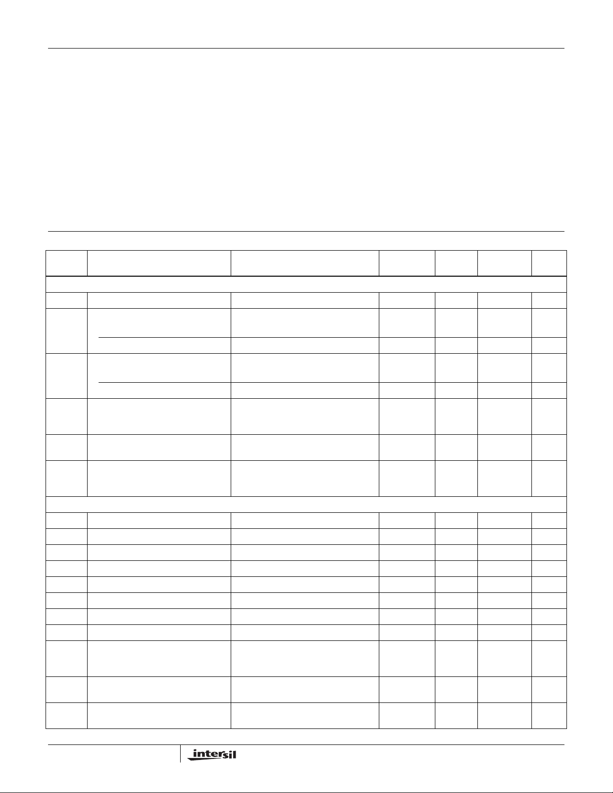
Analog Specifications V
= 5.5V, TA= +25°C to +85°C, Unless Otherwise Noted
CC
TYP
SYMBOL PARAMETER TEST CONDITIONS MIN
(Note 2) MAX UNITS
POWER SUPPLY
V
I
Q(NV)
Vpor Power-on Recall Voltage
V
Ramp
Supply Voltage Range 2.7 3.0 5.5 V
CC
I
Supply
Q
= 2.7V Standby, SDA = SCL = V
V
CC
V
= 5.5V Standby, SDA = SCL = V
CC
CC
CC
200 400 µA
235 500 µA
Non-Volatile Supply
= 2.7V Nonvolatile write 500 750 µA
V
CC
V
= 5.5V Nonvolatile write 1.3 1.6 mA
CC
2.0 2.6 V
CC
t
D
Minimum V
occurs
Ramp Rate 0.2 V/ms
V
CC
Power-Up Delay
V
above Vpor, time delay to Register
CC
recall, and I
at which memory recall
CC
2
C Interface in standby state
3ms
OUTPUT VOLTAGE PERFORMANCE SPECIFICATIONS
G
G
Gain Error AV = 2 (Notes 1, 3, 12) -1 +1 %
E1
Gain Error AV = 4 (Notes 1, 3, 12) -1 +1 %
E2
K Temperature Sensor Coefficient (Notes 1, 8) -2.2 -2.1 -2.0 mV/°C
Absolute Output Voltage (Swing) Range Unloaded, T
Absolute Output Voltage (Swing) Range Loaded, I
TS1 Temperature Sensor Slope A
TS2 Temperature Sensor Slope A
TS3 Temperature Sensor Slope A
TS4 Incremental Temperature Sensor Slope A
= 1, n = 255, m = 255 (Notes 1, 6) -2.1 mV/°C
V
= 2, n = 255, m = 255 (Notes 1, 6) -4.2 mV/°C
V
= 4, n = 255, m = 255 (Notes 1, 6) -8.4 mV/°C
V
= 1, n = 255, m = 0 to 255 (Notes 1,
V
= +25°C (Note 3) VCC - 0.100 GND + 0.100 V
A
= ±500µA (Note 3) VCC - 0.250 GND + 0.250 V
OUT
8.2 μV/°C
10)
TSNL Temperature Slope Non-Linearity n = 255, m = 0 to 255, T = -40°C to +85°C
±0.5 ±1.0 %
(Notes 1, 11)
DNL DAC Relative Linearity
(V
= 2.7 to 5.5V)
CC
and Temp Sense; AV = 1 (Note 13) -1.0 +1.0 LSB
V
REF
per
Code
3
FN8091.1
April 24, 2007
ISL21400
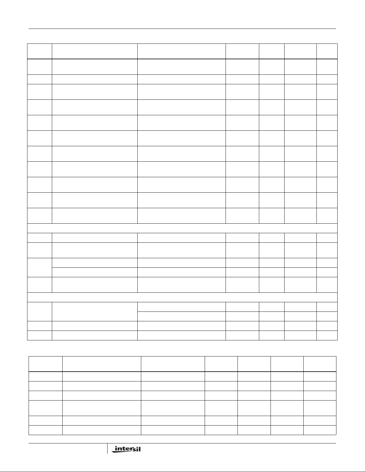
Analog Specifications V
= 5.5V, TA= +25°C to +85°C, Unless Otherwise Noted
CC
SYMBOL PARAMETER TEST CONDITIONS MIN
INL DAC Absolute Linearity (VCC = 2.7 to
V
and Temp Sense; AV = 1 (Note 13) -3.0 +3.0 LSB
REF
5.5V)
V
OUT(TE)
V
V
V
V
OUT1
OUT2
OUT3
OUT4
Total Error for V
Output Voltage V
Output Voltage V
Output Voltage V
Output Voltage V
OUT
, Gain = 1 AV = 1, n = 255, m = 128, TA=+25°C,
REF
, Gain = 2 AV = 2, n = 255, m = 128, TA=+25°C,
REF
, Gain = 4 AV = 4, n = 255, m = 128, TA=+25°C,
REF
+ TS AV = 1, n = 255, m = 0, TA = +85°C
REF
(Notes 1, 8, 9) ±1 ±2 %
V
=5.5V
CC
V
=5.5V
CC
V
=5.5V
CC
1.189 1.2 1.211 V
2.378 2.40 2.422 V
4.756 4.80 4.844 V
1.315 1.326 1.337 V
(Note 3)
V
V
V
OUT5
OUT6
OUT7
Output Voltage V
Output Voltage V
Output Voltage V
+ TS AV = 1, n = 255, m = 128, TA=+85°C
REF
+ TS AV = 1, n = 255, m = 255, TA=+85°C
REF
+ TS AV = 1, n = 255, m = 0, TA= -40°C,
REF
(Note 3)
(Note 3)
1.188 1.199 1.210 V
1.063 1.074 1.085 V
1.052 1.063 1.074 V
(Note 3)
V
V
OUT8
OUT9
Output Voltage V
Output Voltage V
+ TS AV = 1, n = 255, m = 128, TA= -40°C,
REF
+ TS AV = 1, n = 255, m = 255, TA= -40°C,
REF
(Note 3)
1.189 1.200 1.211 V
1.336 1.325 1.347 V
(Note 3)
OUTPUT VOLTAGE DC SPECIFICATIONS
PSRR Power Supply Rejection Ratio A
R
Output Impedance (load regulation) Given by R
OUT
I
Short Circuit, Sourcing V
SC
Short Circuit, Sinking V
C
Load Capacitance Reference output stable for all CL up to
L
= 1, n = 255, m = 128, (Note 7) 50 60 dB
V
T
= +25°C, I
A
= 5.5V, V
CC
= 5.5V, V
CC
OUT
= (ΔV
OUT
OUT
OUT
/ΔI
OUT
),
OUT
= ±500µA
= 0V 5 9 mA
= 5.5V 6 9 mA
specifications
OUTPUT VOLTAGE AC SPECIFICATIONS
Output Voltage Noise 0.1Hz to 10Hz, AV =1 90 µV
V
N
10Hz to 10kHz, CL = 0, AV = 1 TBD mV
Power On Response 1% Settling 500 µs
Line Ripple Rejection V
= 5V ±100mV, f = 120Hz 60 dB
CC
TYP
(Note 2) MAX UNITS
25Ω
5nF
P-P
RMS
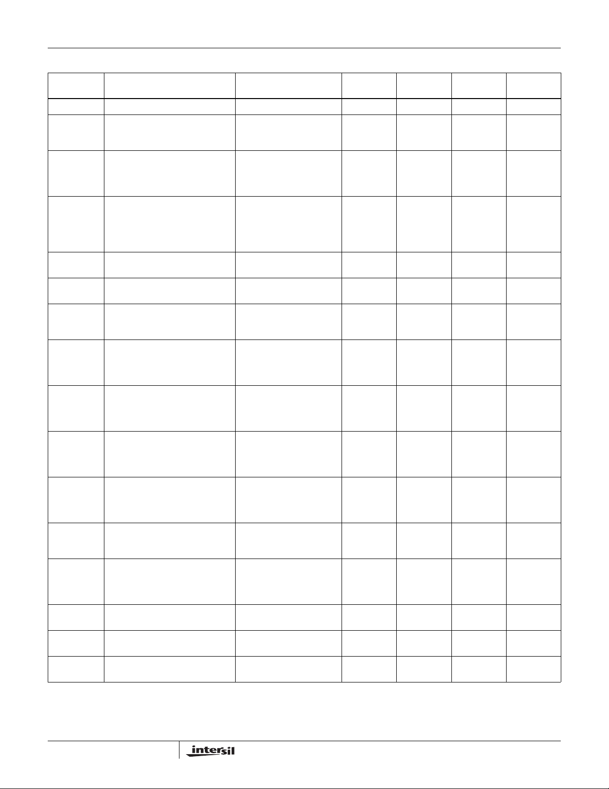
Serial Interface Specification (for SCL, SDA, A0, A1, A2 unless specified otherwise)
SYMBOL PARAMETER TEST CONDITIONS MIN
I
LI
V
IL
V
IH
Hysteresis SDA and SCL Input Buffer
V
OL
C
pin
Input Leakage VIN = GND to V
CC
Input LOW Voltage -0.3 0.3 x V
Input HIGH Voltage 0.7 x V
0.05 x V
Hysteresis
SDA Output Buffer LOW Voltage IOL = 3mA 0 0.4 V
Pin Capacitance (Note 3) 10 pF
4
CC
CC
TYP
(Note 2) MAX UNITS
1V
CC
V
+ 0.3 V
CC
V
V
FN8091.1
April 24, 2007
ISL21400
Serial Interface Specification (for SCL, SDA, A0, A1, A2 unless specified otherwise) (Continued)
SYMBOL PARAMETER TEST CONDITIONS MIN
f
SCL
t
sp
SCL Frequency (Note 3) 400 kHz
Pulse Width Suppression Time at
SDA and SCL Inputs
Any pulse narrower than the
max spec is suppressed
(Note 3)
t
AA
SCL Falling Edge to SDA Output
Data Valid
SCL falling edge crossing
30% of V
the 30% to 70% of V
, until SDA exits
CC
CC
window (Note 3)
t
BUF
Time the Bus Must be Free Before
the Start of a New Transmission
SDA crossing 70% of VCC
during a STOP condition, to
SDA crossing 70% of V
during the following START
CC
1300 ns
condition (Note 3)
t
LOW
t
HIGH
Clock LOW Time Measured at the 30% of VCC
crossing (Note 3)
Clock HIGH Time Measured at the 70% of VCC
1300 ns
600 ns
crossing (Note 3)
t
SU:STA
t
HD:STA
t
SU:DAT
START Condition Setup Time SCL rising edge to SDA
falling edge; both crossing
70% of V
(Note 3)
CC
START Condition Hold Time From SDA falling edge
crossing 30% of V
falling edge crossing 70% of
V
(Note 3)
CC
CC
to SCL
Input Data Setup Time From SDA exiting the 30% to
70% of V
window, to SCL
CC
600 ns
600 ns
100 ns
rising edge crossing 30% of
V
(Note 3)
CC
t
HD:DAT
t
SU:STO
t
HD:STO
t
DH
Input Data Hold Time From SCL rising edge
crossing 70% of V
entering the 30% to 70% of
V
window (Note 3)
CC
CC
STOP Condition Setup Time From SCL rising edge
STOP Condition Hold Time for
Read, or Volatile Only Write
crossing 70% of V
rising edge crossing 30% of
V
(Note 3)
CC
From SDA rising edge to SCL
falling edge; both crossing
70% of V
(Note 3)
CC
, to SDA
CC
Output Data Hold Time From SCL falling edge
crossing 30% of V
CC
to SDA
, until
0ns
600 ns
1300 ns
0ns
SDA enters the 30% to 70%
of V
window (Note 3)
CC
t
R
SDA and SCL Rise Time From 30% to 70% of VCC
20 + 0.1 x Cb 250 ns
(Note 3)
t
F
Cb Capacitive Loading of SDA or SCL Total on-chip and off-chip
SDA and SCL Fall Time From 70% to 30% of VCC
(Note 3)
20 + 0.1 x Cb 250 ns
10 400 pF
(Note 4)
(Note 2) MAX UNITS
TYP
50 ns
900 ns
5
FN8091.1
April 24, 2007
ISL21400
Serial Interface Specification (for SCL, SDA, A0, A1, A2 unless specified otherwise) (Continued)
SYMBOL PARAMETER TEST CONDITIONS MIN
1kΩ
Rpu SDA and SCL Bus Pull-up Resistor
Off-chip
Maximum is determined by t
and t
F
For Cb = 400pF , max is about
R
2~2.5kΩ
For Cb = 40pF, max is about
15~20kΩ
I
V
V
LO
IL
IH
Output Leakage Current (SDA only) V
A1, A0, SHDN, SDA, and SCL Input
Buffer LOW Voltage
A1, A0, SHDN, SDA, and SCL Input
= GND to V
OUT
CC
-0.3 VCC x 0.3 V
VCC x 0.7 V
Buffer HIGH Voltage
V
OL
C
SDA Output Buffer LOW Voltage IOL = 100µA (Note 3), at 3mA
sink
Capacitive Loading of SDA or SCL Total on-chip and off-chip
L
(Note 3)
00.4V
10 400 pF
EEPROM Endurance 1,000,000 Cycles
t
WC
(Note 14)
EEPROM Retention Temperature T
Non-Volatile Write Cycle Time 12 20 ms
≤ +55°C 50 Years
(Note 2) MAX UNITS
TYP
1µA
CC
V
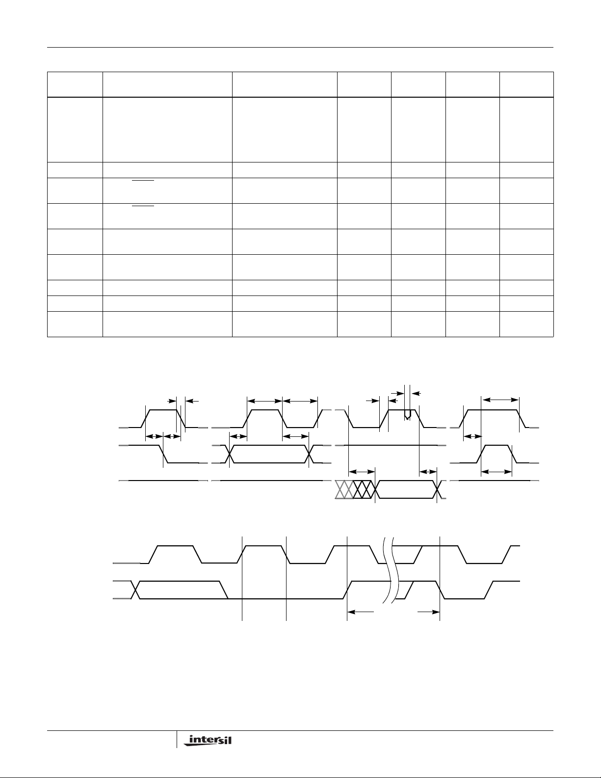
Timing Diagrams
Bus Timing
t
F
SCL
(INPUT TIMING)
(OUTPUT TIMING)
SDA
SDA
t
SU:STA
t
HD:STA
t
SU:DAT
Write Cycle Timing
SCL
SDA
NOTES:
1. Equation 1 governs the output voltage and is stated as follows:
V
2. Typical values are for T
8th BIT OF LAST BYTE ACK
⎧⎫
• n = 0 to 255, m = 0 to 255, K = -2.1mV/C(typ), T0 = +25°C,=
OUTAVVREF
⎨⎬
⎩⎭
= +25°C and VCC = 5.5V.
A
n
--------- -
• KT T
+
255
t
HIGH
2m•()255–
--------------------------------
–()
0
255
t
LOW
t
HD:DAT
STOP
CONDITION
t
t
DH
sp
START
CONDITION
t
BUF
t
HD:STO
t
SU:STO
t
R
t
AA
t
WC
6
FN8091.1
April 24, 2007

ISL21400
3. This parameter is not 100% tested.
4. Cb = total capacitance of one bus line in pF.
is the time from a valid stop condition at the end of a write sequence to the end of the self-timed internal nonvolatile write cycle. It is the
5. t
WC
minimum cycle time to be allowed for any nonvolatile write by the user.
6. Over the specified temperature range. Temperature slope (TS) is measured by the box method whereby the change in V
temperature range; in this case, -40°C to +85°C = +125°C. TS
V
------------------------------------------------------------------------------- -
TS
=
OUT
, TS2, TS3 =.
1
Tmin()V
Tmin Tmax–
OUT
Tmax()–
OUT
is divided by the
7. Given by PSRR (dB) = 20 * log
(ΔVout/ΔVCC) at DC.
10
8. Test +25°C and +85°C only.
9. Total error of Equation 1 @ A
=1, K = -2.1mV/°C, V
V
TE()
V
OUT
10. Over the specified temperature range. Temperature slope (TS) is measured by the box method whereby the change in V
temperature range. Incremental TS is the temperature slope at m = 255 minus the temperature slope at m = 0 divided by 255 with A
Tmin()V
V
⎛⎞
OUT
TS4
------------------------------------------------------------------------------- -
⎜⎟
⎝⎠
Tmin Tmax–()
= 1.20V, m = 255, n = 255 to 0, VCC = 3.0V.
REF
measured()V
V
OUT
-------------------------------------------------------------------------------------------------------------
Tmax()–
OUT
m 255=
V
Equation1()
OUT
⎛⎞
– 255÷=
⎜⎟
⎝⎠
Equation1()–
OUT
V
Tmin()V
OUT
------------------------------------------------------------------------------- -
Tmin Tmax–()
OUT
x100%=
is divided by the
OUT
= 1, n = 255
V
Tmax()–
m0=
11. Temperature Slope Non- linearity is measured over the specified temperature range. The actual change in output voltage is subtracted from the
expected change in output voltage, and then divided by the expected change to normalize before converting to percent.
ΔT )()ΔVOUT–
T( S
y
TSNL
----------------------------------------------------------
TS
ΔT×
y
x100%; y 123,,==
12. For codes n = 8 to 255
13. Guaranteed monotonic
is the time from a valid STOP condition at the end of a Write sequence of I2C serial interface, to the end of the self-timed internal nonvolatile
14. t
WC
write cycle.
15. θ
is measured with the component mounted on a high effective thermal conductivity test board in free air. See Tech Brief TB379 for details.
JA
Typical Performance Curves
3.0
2.5
2.0
TS = 0
(V)
1.5
REF
V
1.0
TS = 0
0.5
0.0
-40 -15 10 35 60 85
FIGURE 1. V
AV = 2
TS = 127
= 1
A
V
TEMPERATURE (°C)
vs TEMPERATURE (AV = 1, 2) FIGURE 2. V
OUT
TS = 255
TS = 255
TS = 127
6.0
5.5
5.0
(V)
4.5
REF
V
4.0
3.5
3.0
-40 -15 10 35 60 85
AV = 4
TS = 127
TS = 0
TEMPERATURE (°C)
vs TEMPERATURE (AV = 4)
OUT
TS = 255
7
FN8091.1
April 24, 2007

Typical Performance Curves (Continued)
ISL21400
1.22
V
REGISTER = 255d
REF
TS REGISTER = 127d
1.21
1.20
VREF (V)
1.19
1.18
2.0 2.5 3.0 3.5 4.0 4.5 5.0 5.5 6.0
V
(V)
CC
FIGURE 3. V
NO LOAD
A
= 1
V
100µV/DIV (V
OUT
vs V
OUT
x 1000)
CC (VCC
= +2.7V to +5.5V) FIGURE 4. SUPPLY VOLTAGE vs SUPPLY CURRENT
0.40
0.35
0.30
0.25
0.20
(mA)
CC
I
0.15
0.10
0.05
NO LOAD
= 4
A
V
50µV/DIV (V
REGISTER = 255d
V
REF
TS REGISTER = 127d
0
2456
OUT
3
x 1000)
+85°C
+25°C
-40×C
-40°C
(V)
V
CC
7
FIGURE 5. V
1.22
1.21
(V)
1.20
REF
V
1.19
1.18
-40 -15 10 35 60 85
VOLTAGE NOISE (AV = 1, NO LOAD) FIGURE 6. V
OUT
V
REGISTER = 255d
REF
TS REGISTER = 127d
TEMPERATURE (°C)
VOLTAGE NOISE (AV = 4, NO LOAD)
OUT
FIGURE 7. ACCURACY vs TEMPERATURE (-40°C TO +85°C) FIGURE 8. POWER ON
8
CH1 = V
CH2 = V
CC
OUT
FN8091.1
April 24, 2007

Typical Performance Curves (Continued)
5
ISL21400
3
2
1
0
-1
INL IN LSB
-2
-3
0 15 30 45 60 75 90 105 120 135 150 165 180195210 225 240 255
FIGURE 9. INL, V
1.4
AT +25°C
TS REGISTER = 127d
1.2
1.0
0.8
(V)
REF
0.6
V
0.4
0.2
0.0
0 15 30 45 60 75 90 105120 135 150 165 180 195 210 225 240 25
FIGURE 11. V
REF
V
REGISTER CODE (m)
REF
OUT
AT +25°C
CODE
AND TEMP SLOPE DAC FIGURE 10. DNL, V
vs V
CODE (m) FIGURE 12. V
REF
1.0
0.8
0.6
0.4
0.2
0.0
-0.2
DNL IN LSB
-0.4
-0.6
-0.8
-1.0
1.40
1.35
1.30
1.25
(V)
1.20
REF
V
1.15
1.10
1.05
1.00
0 15 30 45 60 75 90 105120135 15 0165 180195 210 225240 255
AT +25° C
0 15 30 45 60 75 90 105120 135150 165180 195210225 240255
V
+85°C
vs TEMP SENSE CODE (n), TA = -40°C AND
OUT
+85°C
CODE
AND TEMP SLOPE DAC
REF
REGISTER = 255d
REF
-40°C
TS REGISTER CODE (n)
1.209
1.208
1.207
1.206
1.205
(V)
1.204
REF
V
1.203
1.202
1.201
9
V
REGISTER = 255d
REF
TS REGISTER = 127d
AT +25°C
1.2
-1 -0.5 0 0.5 1
FIGURE 13. V
OUT
I
OUT
vs I
(mA)
OUT
(±1mA)
FN8091.1
April 24, 2007

ISL21400
Pin Descriptions
V
OUT
Programmable voltage output pin. Absolute voltage is
determined by device temperature and Equation 1. Drive
capability is limited to ±500μA output current and 5000pF
output capacitance.
A2, A1, A0
Hardware slave address pins that can be used to provide
several ISL21400 with a unique physical address to allow for
multiple devices off one I
2
C bus.
GND
This is the circuit ground pin. It is common for the V
control signal inputs.
OUT
and
SDA
Serial Data Input/Output. Bidirectional pin used for serial
data transfer. As an output, it is open drain and may be
wire-ored with any number of open drain or open collector
outputs. A pullup resistor is required and the value is
dependent on the speed of the serial data bus and the
number of outputs tied together.
SCL
Serial Clock Input. Accepts a clock signal for clocking serial
data into and out of the device. The SCL line requires a
pull-up resistor whose value is dependent on the speed of
the serial clock bus and the number of inputs tied together.
V
CC
Positive Power Supply. Connect to a voltage supply in the
range of 2.7V<V
best performance, bypass with a 0.1µF capacitor to ground.
If the A
V
gain is set to 4 and V
V
must be set to >5.2V for best output performance.
CC
<5.5V, with minimum noise and ripple. For
CC
approaches 5.0V, then
OUT
Functional Description
Functional Overview
Refer to the Functional Block Diagram on page 2. The
ISL21400 provides a programmable output voltage which
combines both a temperature independent term and a
temperature dependent term. The temperature independent
term uses a bandgap voltage reference, and the
temperature dependent term uses a Proportional To
Absolute Temperature (PTA T) reference, or Temperature
Sensor. Each voltage source is scalable using two DACs via
2
the I
C serial bus. The resulting output voltage can vary from
0V to over 5V and has a variable, programmable
Temperature Slope (TS).
Reference Sections
Referring to the Block Diagram on page 2, the V
Temperature Sense (V
) outputs are summed together (Σ)
TS
and then passed through the output gain stage (A). The
voltage output is programmable and is determined by the
Equation 1:
V
OUTAVVREF
⎧⎫
•=
⎨⎬
⎩⎭
n
--------- -
• V
+
255
2m•()255–
--------------------------------
TS
255
where
•A
= 1, 2, 4
V
•V
= 1.200 (not temperature dependent)
REF
•0 ≤ n ≤ 255 (setting contained in Register 0, V
•V
= K(T - T0)
TS
•K = dV
/ dT = -2.1mV/C
TS
• T = device temperature
•T0 = +25°C
•0 ≤ m ≤ 255 (setting contained in Register 1, TS)
See “Applications Information” on page 14 for ways to use
Equation 1 and methods for output voltage calculations.
REF
REF
and
(EQ. 1)
)
DACs Section
The ISL21400 contains two 8-bit DACs whose registers can
be programmed via the I
are non-volatile such that the values are restored during the
V
power-up cycle of the device. One DAC (V
CC
dedicated to scale the bandgap voltage reference
(Temperature invariant) and the other DAC (V
dedicated to scale the Temperature Sensor. Both of these
DACs can determine the output voltage as defined by
Equation 1 (See “Register Descriptions” on page 11.).
2
C serial bus. The DAC registers
) is
REF
) is
TS
Output Gain Amplifier Section
The ISL21400 contains an output gain amplifier (A) that is
programmed via the I
last stage before the output and therefore controls the
overall gain for the device. The gain can be programmed for
1x, 2x, or 4x amplification. This gain factor is used to
program the output voltage as determined by Equation 1
(See “Register Descriptions” on page 11.).
There are 5 registers in the ISL21400 device, all nonvolatile
(see Table 2). All register s are accessible for reading or
writing through the I
2
C serial bus. The gain amplifier is the
2
C serial bus.
10
FN8091.1
April 24, 2007

ISL21400
Register Descriptions
TABLE 1. ISL21400 REGISTER BIT MAP
D7
Addr
0V
1 TS7 TS6 TS5 TS4 TS3 TS2 TS1 TS0
2 D7D6D5D4D3D2GAIN1GAIN0
3 D7D6D5D4D3D2D1D0
4 D7D6D5D4D3D2D1D0
(MSB)D6D5D4D3D2D1D0(LSB)
7V
REF
6V
REF
5V
REF
4V
REF
3V
REF
2V
REF
1V
REF
REF
0
TABLE 2. REGISTER DESCRIPTIONS
REG NONVOLATILE DESCRIPTION
0 Y Reference setting
1 Y Temperature Sensor setting
2 Y Gain and storage
3 Y Storage
4 Y Storage
Register 0: Bandgap Reference Gain (Nonvolatile)
Register 0 sets the output voltage of the bandgap reference
(V
). Referring to Equation 1, the number “n” is the setting
REF
from Register 0 as follows:
n
--------- -
V
• , for n = 0 to 255
REF
255
This term of Equation 1 can vary from 0V to 1.20V.
Register 1: Temperature Slope Gain (Nonvolatile)
Register 1 sets the Temperature Slope (TS) of the
temperature sensor. Referring to Equation 1, the number “m”
is the setting from Register 1 as follows:
2m•()255–
--------------------------------
V
TS
255
V
is the temperature dependent term and varies from
TS
+136mV at -40°C to -126mV at +85°C. The other term varies
from -1 to +1 and scales the temp erature t erm before add ing
to the V
REF
portion.
Register 2: Device Gain and Storage (nonvolatile)
TABLE 3. REGISTER 2 OUTPUT GAIN (NONVOLA TILE):
GAIN1 GAIN0 OUTPUT GAIN, A
Register 2 contains 2 bits (2 LSB’s) which control the output
gain of the device. Table 3 shows the state of these two bits
OUTPUT GAIN
V
00 x 1
01 x 2
10 x 2
11 x 4
and the resulting output gain. Note that two states produce
the same gain (Gain 1:0 set to 01b and 10b) of x2.
The other 6-bits in the register can be used for general
purpose memory (nonvolatile) or left alone.
Registers 3 and 4: general purpose data
(nonvolatile)
These two registers are one byte each and can be used for
general purpose nonvolatile memory.
I2C Serial Interface
The ISL21400 supports a bidirectional bus oriented protocol.
The protocol defines any device that sends data onto the
bus as a transmitter and the receiving device as the receiver.
The device controlling the transfer is the master and the
device being controlled is the slave. The master always
initiates data transfers and provides the clock for both
transmit and receive operations. Therefore, the ISL21400
operates as a slave device in all applications.
All communication over the I
sending the MSB of each byte of data first.
Protocol Conventions
Data states on the SDA line can change only during SCL
LOW periods. SDA state changes during SCL HIGH are
reserved for indicating START and STOP conditions (See
Figure 10). On power-up of the ISL21400 the SDA pin is in
the input mode.
2
All I
C interface operations must begin with a START
condition, which is a HIGH to LOW transition of SDA while
SCL is HIGH. The ISL21400 continuously monitors the SDA
and SCL lines for the START condition and does not
respond to any command until this condition is met (See
Figure 10). A START condition is ignored during the powerup sequence and during non-volatile write cycles for the
device.
2
All I
C interface operations must be terminated by a STOP
condition, which is a LOW to HIGH transition of SDA while
SCL is HIGH (See Figure 10) A STOP condition at the end of
a read operation, or at the end of a write operation places
the device in its standby mode. A STOP condition at the end
of a write operation to a non-volatile byte initiates an internal
2
C interface is conducted by
11
FN8091.1
April 24, 2007

ISL21400
non-volatile write cycle. The device enters its standby state
when the internal, non-volatile write cycle is completed.
An ACK, Acknowledge, is a software convention used to
indicate a successful data transfer. The transmitting device,
either master or slave, releases the SDA bus after
transmitting eight bits. During the ninth clock cycle, the
receiver pulls the SDA line LOW to acknowledge the
reception of the eight bits of data (See Figure 11).
The ISL21400 responds with an ACK after recognition of a
START condition followed by a valid Identification Byte, and
once again after successful receipt of an Address Byte. The
ISL21400 also responds with an ACK after receiving a Data
Byte of a write operation. The master must respond with an
ACK after receiving a Data Byte of a read operation.
A valid Identification Byte contains 0101 A2 A1 A0 as the
seven MSBs. The A2 A1 A0 bits must correspond to the
logic levels at those pins of the ISL21400 device. The LSB in
the Read/Write
bit. Its value is “1” for a Read operation, and
“0” for a Write operation (See Table 4).
Write Operation
TABLE 4. IDENTIFICATION BYTE FORMAT
0 1 0 1 A2 A1 A0 R/W
(MSB) (LSB)
A Write operation requires a START condition, followed by a
valid Identification Byte, a valid Address Byte, a Data Byte,
and a STOP condition. After each of the three bytes, the
ISL21400 responds with an ACK. The master will then send
a STOP and at this time the device begins its internal
non-volatile write cycle. During this time, the device ignores
transitions at the SDA and SCL pins, and the SDA output is
at a high impedance state. When the internal non-volatil e
write cycle is completed, the ISL21400 enters its standby
state (see Figure 12).
Read Operation
A Current Address Read operation is shown in Figure 13. It
consists of a minimum 2 bytes: a START followed by the ID
byte from the master with the R/W
followed by the data byte or bytes sent by the slave. The
master terminates the Read operation by not responding
with an ACK and then issuing a STOP condition. This
operation is useful if the master knows the current address
and desires to read one or more data bytes.
A Random Address Read operation consists of a three byte
“dummy write” instruction followed by a Current Address
Read operation (See Figure 14). The master initiates the
operation issuing the following sequence: a START, the
identification byte with the R/W
Byte, a second START, and a second Identification byte with
the R/W
bit set to "1". After each of the three bytes, the
ISL21400 responds with an ACK. The ISL21400 then
transmits Data Bytes as long as the master responds with an
ACK during the SCL cycle following the eighth bit of each
byte. The master terminates the Read operation (issuing a
STOP condition) following the last bit of the last Data Byte
(See Figure 13).
The Data Bytes are from the registers indicated by an
internal pointer. This pointer initial’s value is determined by
the Address Byte in the Read operation instruction, and
increments by one during transmission of each Data Byte.
Address 04h is the last valid data byte, higher addresses are
not available. Data from addresses higher than memory
location 04h will be invalid.
bit set to 1, then an ACK
bit set to "0", an Address
STOP conditions that terminate write operations must be
sent by the master after sending at least 1 full data byte and
its associated ACK signal. If a STOP byte is issued in the
middle of a data byte, or before 1 full data byte + ACK is
sent, then the ISL21400 resets itself without performing the
write. The contents of the array are not affected.
Data Protection
A valid Identification Byte, Address Byte, and total number of
SCL pulses act as a protection for the registers. A STOP
condition also acts as a protection for non-volatile memory.
During a Write sequence, the Data Byte is loaded into an
internal shift register as it is received. The presence of the
STOP condition after the rest of the bits are received then
triggers the non-volatile write.
12
FN8091.1
April 24, 2007

SCL
SDA
ISL21400
SCL FROM
MASTER
SDA OUTPUT FROM
TRANSMITTER
SDA OUTPUT
FROM RECEIVER
SIGNALS FROM THE
MASTER
START DATA DATA STOP
STABLE CHANGE
DATA
STABLE
FIGURE 14. VALID DATA CHANGES, START AND STOP CONDITIONS
81 9
HIGH
HIGH
START ACK
FIGURE 15. ACKNOWLEDGE RESPONSE FROM RECEIVERFIGURE 15. ACKNOWLEDGE RESPONSE FROM RECEIVER
WRITE
S
T
IDENTIFICATION
A
BYTE WITH R/W
R
T
= 0
ADDRESS
BYTE
DATA
BYTE
S
T
O
P
SIGNAL AT SDA
SIGNALS FROM THE
ISL21400
00011
A
C
K
000
A0A1A2
0
000
A
C
K
A
C
K
FIGURE 16. BYTE WRITE SEQUENCE
A1 A0
= 1
READ
A
C
FIRST READ DATA
K
BYTE
A
C
K
A
C
K
LAST READ DATA
BYTE
S
T
O
P
FN8091.1
April 24, 2007
SIGNALS
FROM THE
MASTER
SIGNAL AT SDA
SIGNALS FROM
THE SLAVE
S
T
IDENTIFICATION
A
BYTE WITH R/W
R
T
01011
A2
FIGURE 17. ADDRESS READ SEQUENCE
13

V
ISL21400
SIGNALS
FROM THE
MASTER
SIGNAL AT SDA
SIGNALS FROM
THE SLAVE
S
T
A
IDENTIFICATION
R
BYTE WITH R/W
T
00011
= 0
AAA0000 0
ADDRESS
BYTE
A
C
K
FIGURE 18. RANDOM ADDRESS READ SEQUENCE
A
C
K
Applications Information
Power-Up Considerations
The ISL21400 has on-chip EEPROM memory storage for
the DAC and gain settings of the device. These settings
must be recalled correctly on power-up for proper operation.
Normally there are no issues with recall, although it is always
best to provide a smooth, glitch-free power-up waveform on
V
. Adding a small 0.1μF capacitor at the device VCC will
CC
help with power-up as well as V
Noise Performance
The output noise voltage in a 0.1Hz to 10Hz bandwidth is
typically 90µV
. The noise measurement is made with a
P-P
bandpass filter made of a 1 pole high-pass filter with a corner
frequency at 0.1Hz and a 2-pole low-pass filter with a corner
frequency at 12.6Hz to create a filter with a 9.9Hz
bandwidth. Load capacitance up to 5000pF can be added
but will result in only marginal improvements in output noise
and transient response. The output stage of the ISL21400 is
not designed to drive heavily capacitive loads. For high
impedance loads, an R-C network can be added to filter high
frequency noise and preserve DC control.
Output Voltage Programming Considerations
Setting and controlling the output voltage of the ISL21400
can be done easily by breaking down the components into
temperature variant and invariant, and setting them
separately. Let’s use Equation 1 to derive separate
Reference Output and Output Temp Slope equations:
V
⎧⎫
AVV
•
⎨⎬
OUT
⎩⎭
• A
A
VVREF
Reference Term Temp Slope Term+
The first term controls the output DC value, and the second
term controls the Temp slope, where
n
A
A
--------- -
= (ranges from 0 to 1)
REF
255
2m•()255–
⎛⎞
----------------------------------
TS
⎝⎠
255
n
--------- -
•
REF
255
•{}= AVV•
REF
(ranges from -1 to +1)=
+=
load changes.
OUT
⎧⎫
A
⎨⎬
V
⎩⎭
2m•()255–
⎛⎞
----------------------------------
V•
•
⎝⎠
TS
TS
255
ATS•{}""+
S
T
A
IDENTIFICATION
R
BYTE WITH R/W
T
01011
S
T
O
P
AAA
= 1
A
C
FIRST READ
K
DATA BYTE
A
A
C
C
K
K
LAST READ
DATA BYTE
DC OUTPUT CONTROL DISCUSSION
The reference term yields Equation 2 for Reference Output:
V
OUT
(DC) A=
V
• A
REF
V
•
REF
(EQ. 2)
Note that the DC term is dependent on the 1.20V reference
voltage, which is constant, the overall gain, A
Reference gain, A
. Since the product AV * A
REF
, and the
V
REF
ranges
from 0 to 4, the total reference DC output can range from
0.0V to 4.8V. In order to get the 4.8V output, V
must be
CC
greater than 4.8V by the output dropout plus any overhead
for output loading (the specification for V
with V
changes with A
(A
V
A
V
= 5.5V). The Resolution of V
CC
, so that with a 4.80V full scale output
V
= 4), the resolution is 4.80/255 or 18.8mV/bit. With
= 1, the resolution is 4.7mV/bit.
= 5.0V is listed
OUT
(DC) control
OUT
TEMP SENSE CONTROL DISCUSSION
Equation 2 yields this expression, Equation 3, for Temp
Slope:
OUT
Since V
TS() AVVTS• ATS•=
= K(T - T0), the slope term is dependent on the
TS
(EQ. 3)
base temp slope of the device, K (-2.1mV/°C), and the gain
terms A
portion of V
V
OUT
The product A
and ATS. This gives a formula (Equation 4) for the
V
TS()AVK• ATS• TT0–()•=
at a specific temperature:
OUT
ranges from -4 to 4, so the T emperature
V*ATS
(EQ. 4)
Slope can range from -8.4 to +8.4mV/°C, which is
independent of the output DC voltage. The resolution of
Slope control is determined by this range (±8.4mV/°C) and
the gain terms, and will vary from 65.8μV/°C/bit (A
down to 16.2μV/°C/bit (A
At T = T0 = +25°C, V
cause a change in V
V
(DC) control. As temperature increases or decreases,
OUT
from T = +25°C, V
OUT
= 1).
V
(TS) = 0, no changes in ATS will
OUT
OUT
, and V
will only vary with the
OUT
will then change according to the
= 4)
V
programmed Temp Slope.
14
FN8091.1
April 24, 2007

ISL21400
In many cases a form of Equation 4 is needed which yields a
V
change with respect to temperature. By rearranging,
OUT
we get:
TS()
V
OUT
V
OUT
-----------------------------
T()
= A
TT
–()
0
K• ATS• ,(in mV/° C)=
V
(EQ. 5)
EXAMPLE 1: PROGRAMMED TEMPERATURE
COMPENSATION EXAMPLE
The ISL21400 can easily compensate for known
temperature drift by programming the device for the initial
V
setting and Tempco using standard equations and
OUT
some simple steps. The accuracy of the final programmed
output will be limited to the data sheet specs (typically 1%
accuracy for V
and Slope).
OUT
In this example, an N-Channel MOSFET gate has a
-2.8mV/°C Tempco from -10°C to +85°C. A constant bias
drain current is desired, with a target Vgs range derived from
the data sheet of 2.5V to 3.5V at +25°C.
Offset Setting: Using Equation 2 and targeting
V
= 3.0VDC:,
OUT
V
DC()AVV
OUT
Note that A
AREF()
n 159 decimal=
== =
9F hex=
• A
•()= 3.00V=
REF
REF
V
A
VAREF
REF
2.50
-----------
4
1.20V=
REF
• 2.50=
varies from 0 to 1, so to get 2.40, AV = 4.
n
0.625
--------- -
255
Temperature Slope Setting: Using Equation 5, which can
solve for Slope directly:
T() AVK• ATS•= 2.8mV °C⁄–=
V
OUT
2.8–
--------------------
A
=
TS
42.1–•
2m•()255–
0.333
A
==
TS
m 170 decimal=
A9 hex =
----------------------------------
255
The ISL21400 device can be programmed with these
calculated parameters and perform temperature
compensation or direct control in the target circuit. If
parameters change for some reason, then the device can be
reprogrammed with new values and the circuit retested.
EXAMPLE 2. CALCULATING THE V
TEMPERATURE
OUT
SLOPE
In some applications, it may be desirable to calculate what
the output voltage and temp slope are, given the
programmed register settings. Such an application could be
a closed loop system with internal calibration procedure. By
reading the registers of the ISL21400, then calculating the
V
parameters, the system characteristics can be
OUT
recorded.
For the example below, let’s determine the voltage output,
V
(DC) at +25°C, and also the change due to
OUT
temperature variation (ppm) from +25°C to +85°C.
Equations 2 and 5 will be used to calculate the answers.
Given, the contents of the registers:
A
= 1
V
n = 178 decimal
m = 74 decimal
Using Equation 2:
V
OUT
DC()AVV
=
• A
•()=
REF
REF
⎛⎞
11.20•
⎝⎠
178
--------- -
•
255
0.8376V=
Using Equation 5:
T() AVK• ATS•() mV °C⁄=
V
OUT
274•()255–
12.1
0.8812mV °C⁄=
------------------------------------
•–•=
255
Also, to solve for overall temp slope of the output:
0.8812mV °C⁄
---------------------------------------
872.5mV
6
• 1010ppm °C⁄=
10
Note that Equation 1 can be used directly to solve for output
voltage at a given temperature, in this case +85°C:
⎧⎫
V
OUTAVVREF
V
OUT
•=
⎨⎬
⎩⎭
+85°C()=
=
n
--------- -
• KT T
+
255
1
⎧⎫
178
--------- -
1.20
• 0.0021–()85 25–()
•
⎨⎬
⎩⎭
0.8905V=
255
+
2m•()255–
--------------------------------
–()
0
255
274•()255–
----------------------------------
255
Typical Applications Circuits
LDMOS RF Power Amplifier (RFPA). The ISL21400 is used
to set the gate bias for the LDMOS transistor in a single
stage of an RFPA. Normally this is done with a DAC or digital
potentiometer with some discrete temperature
compensation circuitry. The ISL21400 simplifies this control
and allows a full range of DC bias and tempco control.
A typical circuit can be calibrated for correct bias at room
temperature (+25°C) on power-up using a microcontroller or
2
direct I
increased to the highest operating range, and the
Temperature Slope setting can then be adjusted to bring the
amplifier back to correct bias. Since the Temp Slope setting
has a negligible effect on the room temperature setting, the
amplifier will be biased correctly over the operating
temperature of the unit.
C control. The temperature of the unit can then be
15
FN8091.1
April 24, 2007

ISL21400
2
I
C BUS
+28V
U2
1
IN OUT
2
GND
+5V REGULATOR
5
6
1
2
3
SCL
SDA
A0
A1
A2
A2
ISL21400
VCC
VOUT
GND
3
8
7
4
R1
1k
C1
100pF
RF INPUT
R2
100
C2
FIGURE 19. LDMOS RFPA BIAS CONTROL
+28V
L1
RF OUTPUT
Q1
LDMOS
16
FN8091.1
April 24, 2007

ISL21400
Mini Small Outline Plastic Packages (MSOP)
N
EE1
INDEX
AREA
AA1A2
-H-
SIDE VIEW
12
TOP VIEW
b
e
D
NOTES:
1. These package dimensions are within allowable dimensions of
JEDEC MO-187BA.
2. Dimensioning and tolerancing per ANSI Y14.5M-1994.
3. Dimension “D” does not include mold flash, protrusions or gate
burrs and are measured at Datum Plane. Mold flash, protrusion
and gate burrs shall not exceed 0.15mm (0.006 inch) per side.
4. Dimension “E1” does not include interlead flash or protrusions
and are measured at Datum Plane. Interlead flash and
protrusions shall not exceed 0.15mm (0.006 inch) per side.
5. Formed leads shall be planar with respect to one another within
0.10mm (0.004) at seating Plane.
6. “L” is the length of terminal for soldering to a substrate.
7. “N” is the number of terminal positions.
8. Terminal numbers are shown for reference only.
9. Dimension “b” does not include dambar protrusion. Allowable
dambar protrusion shall be 0.08mm (0.003 inch) total in excess
of “b” dimension at maximum material condition. Minimum space
between protrusion and adjacent lead is 0.07mm (0.0027 inch).
- H -
-A -
.
10. Datums and to be determined at Datum plane
11. Controlling dimension: MILLIMETER. Converted inch dimensions are for reference only.
-B-
0.20 (0.008) A
GAUGE
PLANE
SEATING
PLANE
0.10 (0.004) C
-A-
0.20 (0.008) C
- B -
0.25
(0.010)
-C-
SEATING
PLANE
a
0.20 (0.008) C
- H -
B
4X θ
C
D
4X θ
L1
C
C
L
E
1
END VIEW
R1
R
L
-B-
M8.118 (JEDEC MO-187AA)
8 LEAD MINI SMALL OUTLINE PLASTIC PACKAGE
INCHES MILLIMETERS
SYMBOL
A 0.037 0.043 0.94 1.10 -
A1 0.002 0.006 0.05 0.15 -
A2 0.030 0.037 0.75 0.95 -
b 0.010 0.014 0.25 0.36 9
c 0.004 0.008 0.09 0.20 -
D 0.116 0.120 2.95 3.05 3
E1 0.116 0.120 2.95 3.05 4
e 0.026 BSC 0.65 BSC -
E 0.187 0.199 4.75 5.05 -
L 0.016 0.028 0.40 0.70 6
L1 0.037 REF 0.95 REF -
N8 87
R 0.003 - 0.07 - -
R1 0.003 - 0.07 - -
05
α
o
o
0
15
o
o
6
o
5
o
0
15
o
o
6
Rev. 2 01/03
NOTESMIN MAX MIN MAX
-
-
All Intersil U.S. products are manufactured, assembled and tested utilizing ISO9000 quality systems.
Intersil Corporation’s quality certifications can be viewed at www.intersil.com/design/quality
Intersil products are sold by description only. Intersil Corporation reserves the right to make changes in circuit design, software and/or specifications at any time without
notice. Accordingly, the reader is cautioned to verify that data sheets are current before placing orders. Information furnished by Intersil is believed to be accurate and
reliable. However, no responsibility is assumed by Intersil or its subsidiaries for its use; nor for any infringements of patents or other rights of third parties which may result
from its use. No license is granted by implicat ion or oth erwise u nde r any p a tent or p at ent r ights of Intersil or its subsidiaries.
For information regarding Intersil Corporation and its products, see www.intersil.com
17
FN8091.1
April 24, 2007
 Loading...