

Page 1
查询ISL21007CFB812Z供应商
®
ISL21007
Data Sheet April 12, 2007
Precision, Low Noise FGA™ Voltage
References
The ISL21007 FGA™ voltage references are extremely low
power, high precision, and low noise voltage references
fabricated on Intersil’s proprietary Floating Gate Analog
technology. The ISL21007 features very low noise (4µV
P-P
for 0.1Hz to 10Hz) and very low operating current (150µA,
Max). In addition, the ISL21007 family features guaranteed
initial accuracy as low as ±0.5mV.
This combination of high initial accuracy, low drift, and low
output noise performance of the ISL21007 enables versatile
high performance control and data acquisition applications
with low power consumption.
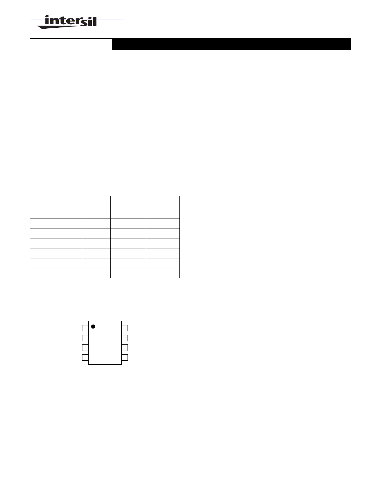
Available Options
ACCURACY
INITIAL
(mV)
TEMPCO.
(ppm/°C)
V
OUT
OPTION
PART NUMBER
ISL21007BFB812Z 1.250 ±0.5 3
ISL21007CFB812Z 1.250 ±1.0 5
ISL21007DFB812Z 1.250 ±2.0 10
ISL21007BFB825Z 2.500 ±0.5 3
ISL21007CFB825Z 2.500 ±1.0 5
ISL21007DFB825Z 2.500 ±2.0 10
(V)
FN6326.1
Features
• Reference Output Voltage . . . . . . . . . . . . . . .1.25V, 2.50V
• Initial Accuracy. . . . . . . . . . . . . . . . . . . .±0.5mV (B grade)
• Input Voltage Range: . . . . . . . . . . . . . . . . . . . 2.7V to 5.5V
• Low Output Voltage Noise . . . . . . 4µV
(0.1Hz to 10Hz)
P-P
• Supply Current. . . . . . . . . . . . . . . . . . . . . . . .150µA (Max)
• Temperature Coefficient. . . . . . . . . . . .3ppm/°C (B grade)
• Operating Temperature Range. . . . . . . . .-40°C to +125°C
• Package. . . . . . . . . . . . . . . . . . . . . . . . . . . . . . 8 Ld SOIC
• Pb-Free Plus Anneal Available (RoHS Compliant)
Applications
• High Resolution A/Ds and D/As
• Digital Meters
• Bar Code Scanners
• Basestations
• Battery Management/Monitoring
• Industrial/Instrumentation Equipment
Pinout
GND or NC
VIN
DNC
GND
ISL21007
(8 LD SOIC)
TOP VIEW
1
2
3
4
8
DNC
7
DNC
6
VOUT
5
TRIM
1
CAUTION: These devices are sensitive to electrostatic discharge; follow proper IC Handling Procedures.
1-888-INTERSIL or 1-888-468-3774
| Intersil (and design) is a registered trademark of Intersil Americas Inc.
All other trademarks mentioned are the property of their respective owners.
Copyright Intersil Americas Inc. 2007. All Rights Reserved
Page 2
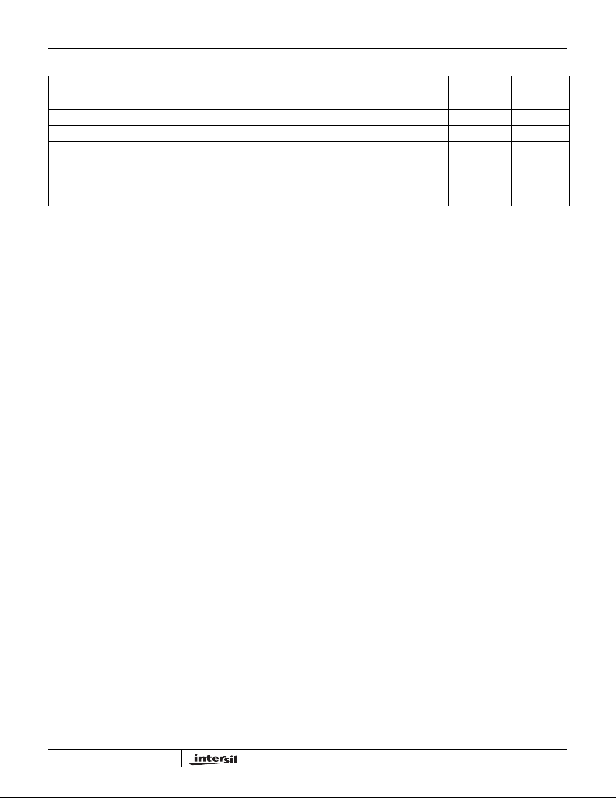
Ordering Information
ISL21007
PART NUMBER
(Note) PART MARKING
ISL21007BFB812Z 21007BF Z12 1.250 ±0.5mV, 3ppm/°C -40 to +125 8 Ld SOIC M8.15
ISL21007CFB812Z 21007CF Z12 1.250 ±1.0mV, 5ppm/°C -40 to +125 8 Ld SOIC M8.15
ISL21007DFB812Z 21007DF Z12 1.250 ±2.0mV, 10ppm/°C -40 to +125 8 Ld SOIC M8.15
ISL21007BFB825Z 21007BF Z25 2.500 ±0.5mV, 3ppm/°C -40 to +125 8 Ld SOIC M8.15
ISL21007CFB825Z 21007CF Z25 2.500 ±1.0mV, 5ppm/°C -40 to +125 8 Ld SOIC M8.15
ISL21007DFB825Z 21007DF Z25 2.500 ±2.0mV, 10ppm/°C -40 to +125 8 Ld SOIC M8.15
NOTE: Intersil Pb-free plus anneal products employ special Pb-free material sets; molding compounds/die attach materials and 100% matte tin plate
termination finish, which are RoHS compliant and compatible with both SnPb and Pb-free soldering operations. Intersil Pb-free products are MSL
classified at Pb-free peak reflow temperatures that meet or exceed the Pb-free requirements of IPC/JEDEC J STD-020.
*Add “-TK” suffix for tape and reel
V
OPTION
OUT
(V) GRADE
TEMP. RANGE
(°C)
PACKAGE
(Pb-Free) PKG. DWG. #
2
FN6326.1
April 12, 2007
Page 3
Pin Descriptions
PIN NUMBER PIN NAME DESCRIPTION
1 GND or NC Ground Connection
2 VIN Power Supply Input Connection
4 GND Voltage Reference Output Connection
5 TRIM Allows user trim ±2.5%
6 VOUT Do Not Connect; Internal Connection – Must Be Left Floating
3, 7, 8 DNC Do Not Connect; Internal Connection - Must Be Left Floating
Typical Application Circuit
ISL21007
SPI BUS
1
+3V
C1
10µF
X79000
1
SCK
2
A0
3
A1
4
A2
5
SI
6
SO
7
/RDY
8
UP
9
DOWN
10
OE
/CS
CLR
VCC
VH
VL
VREF
VSS
VOUT
VBUF
VFB
20
19
18
17
16
15
14
13
12
11
LOW NOISE DAC OUTPUT
GND
2
VIN
3
NC
4
GND
ISL21007-12, 25
FIGURE 1. TYPICAL APPLICATION PRECISION 12-BIT SUBRANGING DAC
NC
NC
VOUT
NC
8
7
6
5
C1
0.001µF
3
FN6326.1
April 12, 2007
Page 4
ISL21007
Absolute Voltage Ratings Thermal Information
Storage Temperature Range . . . . . . . . . . . . . . . . . .-65°C to +150°C
Max Voltage V
Max Voltage V
to Gnd. . . . . . . . . . . . . . . . . . . . . . . -0.5V to +6.5V
IN
to Gnd (10s). . . . . . . . . . . . . . .-0.5V to V
OUT
OUT
+ 1
Voltage on “DNC” pins. . . . No connections permitted to these pins.
Lead Temperature, soldering (10s) . . . . . . . . . . . . . . . . . . . .+260°C
ESD Rating
Human Body Model (HBM) . . . . . . . . . . . . . . . . . . . . . . . . . . .6kV
Machine Model . . . . . . . . . . . . . . . . . . . . . . . . . . . . . . . . . . .600V
Charged Device Model (CDM). . . . . . . . . . . . . . . . . . . . . . . . .2kV
Recommended Operating Conditions
Temperature Range (Industrial). . . . . . . . . . . . . . . .-40°C to +125°C
CAUTION: Stresses above those listed in “Absolute Maximum Ratings” may cause permanent damage to the device. This is a stress only rating and operation of the
device at these or any other conditions above those indicated in the operational sections of this specification is not implied.
IMPORT ANT NOTE: A ll p arameters having Min/Max specificati ons are gua ranteed. Typ values are for informati on purposes only. Unless otherwise noted, all test s are at
the specified temperature and are pulsed tests, theref ore: T
NOTE:
is measured with the component mounted on a high effective thermal conductivity test board in free air. See Tech Brief TB379 for details.
1. θ
JA
= TC = T
J
A
Continuous Power Dissipation (T
8 Lead SOIC derate 5.88mW/°C above +70°C . . . . . . 471mW
= +70°C) (Note 1)
A
Pb-free reflow profile. . . . . . . . . . . . . . . . . . . . . . . . . . see link below
http://www.intersil.com/pbfree/Pb-FreeReflow.asp
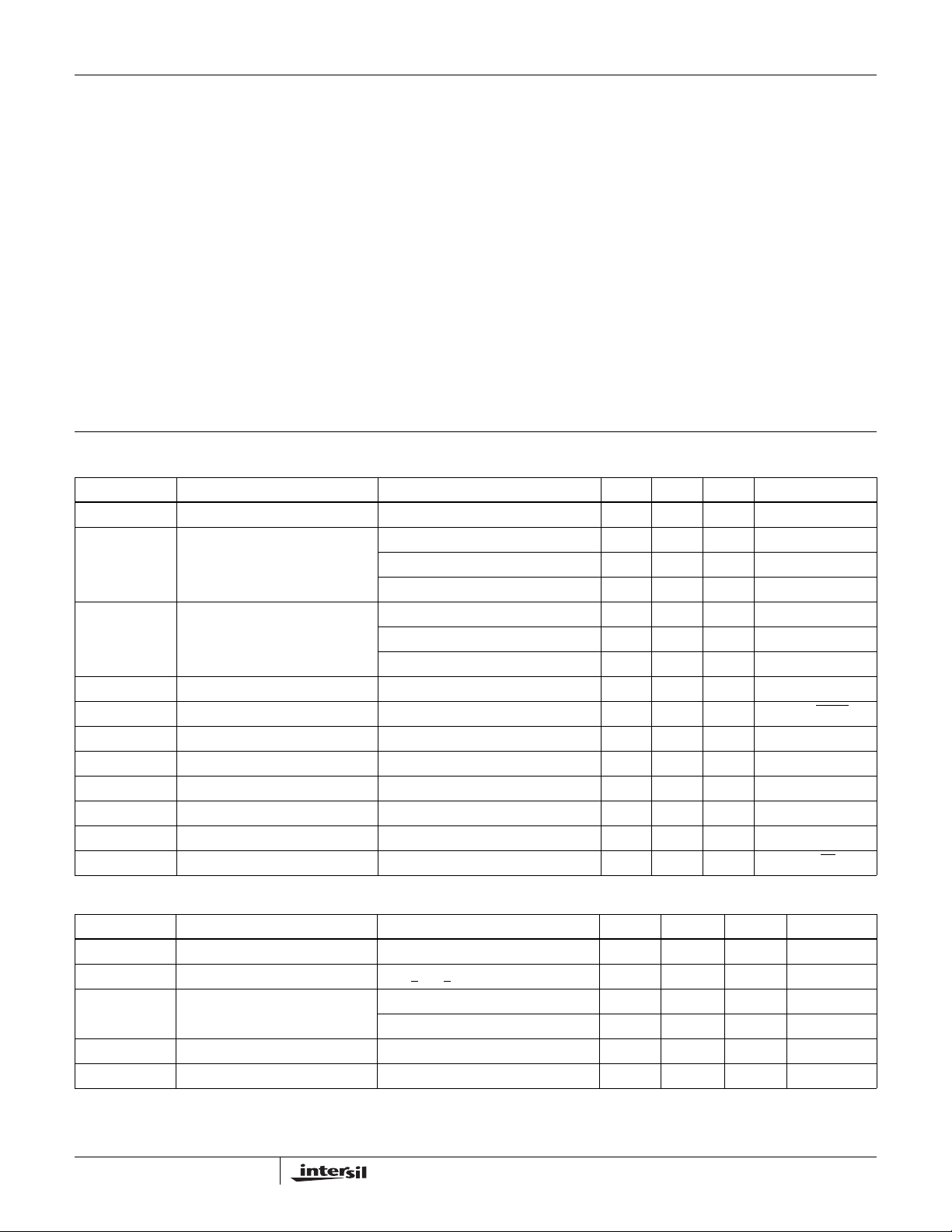
Common Electrical Specifications (ISL21007-12 , -25)T
= -40°C to +125°C, unless otherwise specified.
A
PARAMETER DESCRIPTION CONDITIONS MIN TYP MAX UNIT
V
IN
V
OA
Input Voltage Range 2.7 5.5 V
V
Accuracy @ TA = +25°C ISL21007B -0.5 +0.5 mV
OUT
ISL21007C -1.0 +1.0 mV
ISL21007D -2.0 +2.0 mV
TC V
OUT
Output Voltage Temperature
Coefficient (Note 2)
ISL21007B 3 ppm/°C
ISL21007C 5 ppm/°C
ISL21007D 10 ppm/°C
I
IN
ΔV
/Δt Long Term Stability (Note 4) TA = +25°C TBD ppm/√1kHr s
OUT
Supply Current 75 150 µA
Trim Range ±2.0 ±2.5 %
t
R
Turn on Settling Time V
= ±0.1% 120 µs
OUT
Ripple Rejection f = 10kHz 60 dB
e
N
V
N
Output Voltage Noise 0.1Hz ≤ f ≤ 10Hz 4 µV
Broadband Voltage Noise 10Hz ≤ f ≤ 1kHz 2.2 µV
RMS
Noise Density f = 1kHz 60 nV/√Hz
Electrical Specifications (ISL21007-12, V
= 1.250V) V
OUT
= 3.0V, TA = -40°C to +125°C, unless otherwise specified.
IN
PARAMETER DESCRIPTION CONDITIONS MIN TYP MAX UNIT
V
ΔV
ΔV
I
SC
ΔV
OUT
OUT
OUT
OUT
/ΔV
/ΔI
/ΔT
OUT
A
Output Voltage 1.250 V
Line Regulation 2.7V < VIN < 5.5V 100 700 µV/V
IN
Load Regulation Sourcing: 0mA ≤ I
Sinking: -7mA ≤ I
Short Circuit Current TA = +25°C, V
≤ 7mA 10 100 µV/mA
OUT
≤ 0mA 20 150 µV/mA
OUT
tied to GND 40 mA
OUT
Thermal Hysteresis (Note 3) ΔTA = +165°C 50 ppm
P-P
4
FN6326.1
April 12, 2007
Page 5
ISL21007
Electrical Specifications (ISL21007-25, V
= 2.50V) V
OUT
= 3.0V, TA = -40°C to +125°C, unless otherwise specified
IN
PARAMETER DESCRIPTION CONDITIONS MIN TYP MAX UNIT
V
ΔV
ΔV
I
SC
ΔV
OUT
OUT
OUT
OUT
/ΔV
/ΔI
/ΔT
OUT
Output Voltage 2.500 V
Line Regulation 2.7V < VIN < 5.5V 50 200 µV/V
IN
Load Regulation Sourcing: 0mA ≤ I
Sinking: -5mA ≤ I
Short Circuit Current TA = +25°C, V
Thermal Hysteresis (Note 3) ΔTA = +165°C 50 ppm
A
≤ 5mA 10 100 µV/mA
OUT
≤ 0mA 20 150 µV/mA
OUT
tied to GND 50 mA
OUT
NOTES:
2. Over the specified temperature range. Temperature coefficient is measured by the box method whereby the change in V
is divided by the
OUT
temperature range; in this case, -40°C to +125°C = +165°C.
3. Thermal Hysteresis is the change of V
at T
= +25°C for the device under test. The device is temperature cycled and a second V
A
between the initial V
from +25°C to +125°C to -40°C to +25°C.
reading and the second V
OUT
measured @ TA = +25°C after temperature cycling over a specified range, ΔTA. V
OUT
reading is then expressed in ppm. For Δ TA = +165°C, the device under test is cycled
OUT
measurement is taken at +25°C. The difference
OUT
is read initially
OUT
4. FGA voltage reference long term drift is a logarithmic characteristic. Changes that occur after the first few hundred hours of operation are
significantly smaller with time, asymptotically approaching zero beyond 1,000 hours. Because of this decreasing characteristics, long term drift
is specified in ppm/√1kHrs.
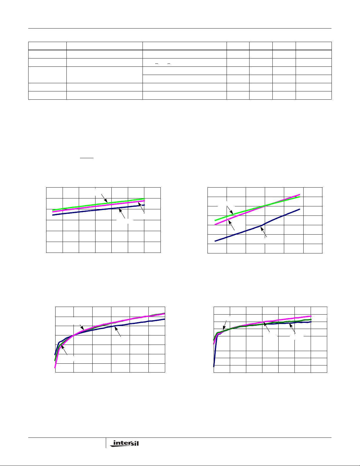
Typical Performance Curves (ISL21007-12) (R
120
100
80
60
(µA)
IN
I
40
20
0
2.5 3.0 3.5 4.0 4.5 5.0 5.5 6.0
FIGURE 2. IIN vs VIN (3 UNITS)
UNIT 3
V
IN
UNIT 1
UNIT 2
(V)
= 100kΩ)
EXT
95
90
+125°C
85
80
75
(µA)
IN
I
70
65
60
2.5 3.0 3.5 4.0 4.5 5.0 5.5
FIGURE 3. I
+25°C
-40°C
V
(V)
IN
vs VIN OVER TEMPERATURE
IN
(V)
OUT
V
1.25015
= 3.0V)
1.25010
IN
1.25005
1.25000
1.24995
1.24990
1.24985
1.24980
(NORMALIZED TO 1.25V A T V
UNIT 3
UNIT 1
2.5 3.0 3.5 4.0 4.5 5.0 5.5
VIN (V)
FIGURE 4. LINE REGULATION (3 UNITS)
5
UNIT 2
150
100
+125°C
50
= 3.0V)
0
IN
-50
-100
(µV)
O
-150
ΔV
-200
-250
(NORMALIZED TO V
-300
2.5 3.0 3.5 4.0 4.5 5.0 5.5 6.0
+25°C
V
-40°C
(V)
IN
FIGURE 5. LINE REGULATION OVER TEMPERATURE
FN6326.1
April 12, 2007
Page 6

ISL21007
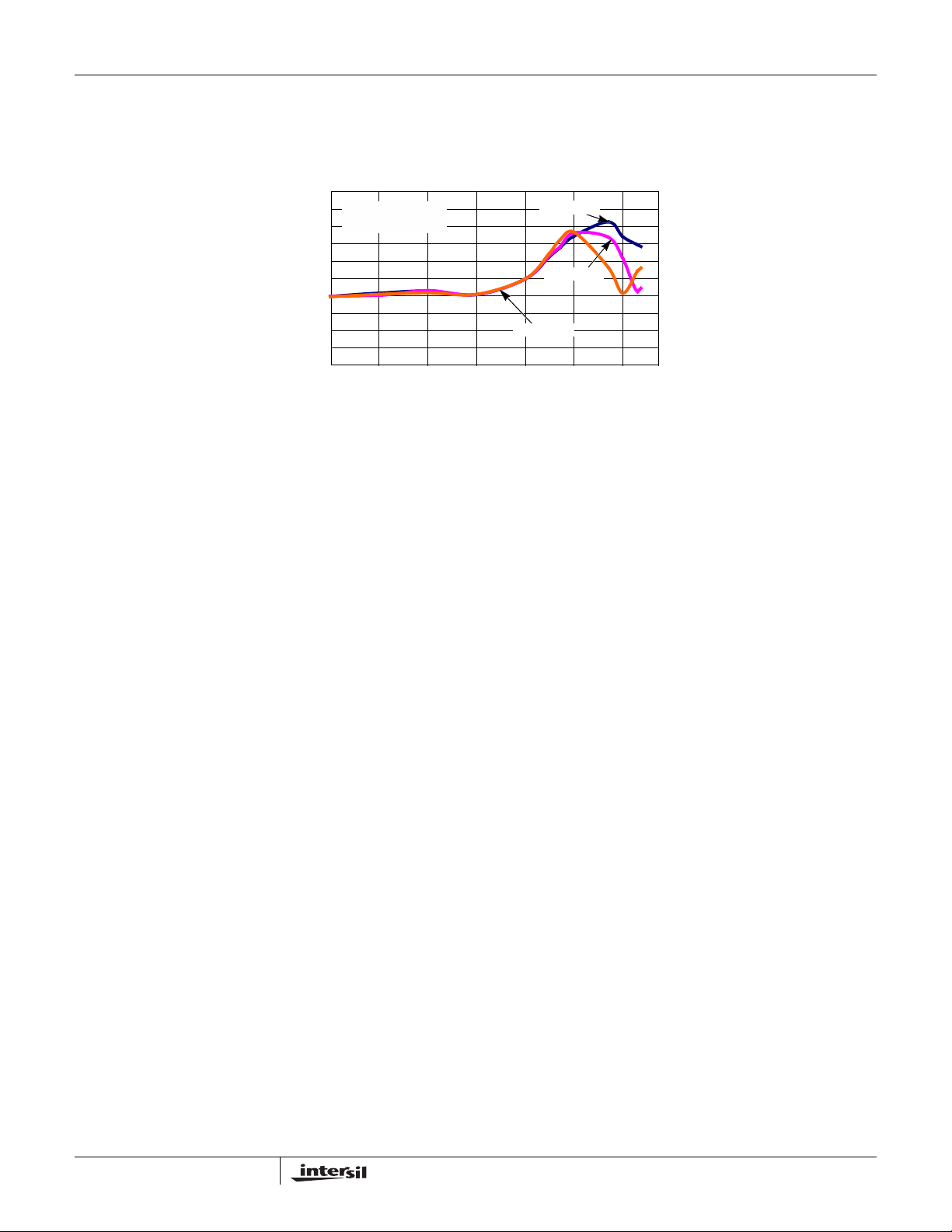
Typical Performance Curves (ISL21007-12) (R
(mV)
OUT
ΔV
0.15
0.10
0.05
0.00
-0.05
-0.10
-0.15
+25°C
-40°C
-7 -6 -5 -4 -3 -2 -1 0 1
SINKING SOURCING
OUTPUT CURRENT (mA)
FIGURE 6. LOAD REGULATION OVER TEMPERATURE
X: 5µs/DIV
Y: 500mV/DIV
+125°C
234567
= 100kΩ) (Continued)
EXT
1.25010
1.25005
1.25000
1.24995
(V)
1.24990
OUT
V
1.24985
1.24980
1.24975
-40 -20 0 20 40 60 80 100 120 140
FIGURE 7. V
UNIT 1
UNIT 3
OUT
X: 5µs/DIV
Y: 500mV/DIV
UNIT 2
TEMPERATURE (°C)
vs TEMPERATURE (3 UNITS)
FIGURE 8. LINE TRANSIENT RESPONSE, NO CAPACITIVE
LOAD
X: 20µs/DIV
Y: 1V/DIV
V
IN
V
= 1.25V (FOR TYP IIN)
OUT
FIGURE 10. TURN ON TIME
FIGURE 9. LINE TRANSIENT RESPONSE, 0.001µF LOAD
CAPACITANCE
120
100
80
(Ω)
60
OUT
Z
40
20
0
1 10 100 1k 10k 100k 1M
FIGURE 11. Z
100100
FREQUENCY (Hz)
OUT
1nF LOAD
10nF LOAD
vs FREQUENCY
NO LOAD
6
FN6326.1
April 12, 2007
Page 7

ISL21007
Typical Performance Curves (ISL21007-12) (R
GAIN IS x1000,
NOISE IS 4µV
2mV/DIV
FIGURE 12. V
p-p
NOISE, 0.1Hz to 10Hz
OUT
0
V
-10
-20
-30
-40
-50
PSRR (dB)
-60
-70
-80
-90
-100
(DC) = 3V
IN
V
(AC) = 50mV
IN
1 10 100 1k 10k 100k 1M
P-P
FREQUENCY (Hz)
FIGURE 14. PSRR vs CAPACITIVE LOADS
= 100kΩ) (Continued)
EXT
NO OUTPUT CAPACITANCE
X: 50µs/DIV
Y: 1V/DIV
FIGURE 13. LOAD TRANSIENT RESPONSE
NO LOAD
1nF LOAD
10nF LOAD
+7mA
-7mA
7
FN6326.1
April 12, 2007
Page 8

ISL21007
Typical Performance Curves (ISL21007-25) (R
120
100
80
60
(µA)
IN
I
40
20
0
2.5 3.0 3.5 4.0 4.5 5.0 5.5 6.0
2.50020
2.50010
2.50000
(V)
2.49990
OUT
V
2.49980
2.49970
2.49960
(NORMALIZED TO 2.5V AT VIN = 3V)
2.5 3.0 3.5 4.0 4.5 5.0 5.5
FIGURE 17. LINE REGULATION (3 UNITS)
UNIT 3
UNIT 1
V
(V)
IN
FIGURE 15. IIN vs VIN (3 UNITS)
UNIT 1
UNIT 3
VIN (V)
UNIT 2
UNIT 2
= 100kΩ)
EXT
100
95
+125°C
90
85
80
(µA)
IN
75
I
70
65
60
2.5 3.0 4.0 4.5 5.0 5.5
FIGURE 16. I
100
50
0
-50
-100
-150
(µV)
-200
O
ΔV
-250
-300
-350
(NORMALIZED TO VIN = 3.0V)
-400
+25°C
2.5 3.0 3.5 4.5 5.0 5.5
-40°C
+25°C
3.5
V
(V)
IN
vs VIN OVER TEMPERATURE
IN
4.0 6.0
V
IN
-40°C
+125°C
(V)
FIGURE 18. LINE REGULATION OVER TEMPERATURE
0.60
0.40
0.20
0.00
-0.20
(mV)
-0.40
OUT
ΔV
-0.60
-0.80
-1.00
-7-6-5-4-3-2-10123456
SINKING SOURCING
+25°C
OUTPUT CURRENT (mA)
+125°C
-40°C
FIGURE 19. LOAD REGULATION OVER TEMPERATURE
8
2.5003
2.5002
2.5001
2.5000
2.4999
(V)
2.4998
OUT
2.4997
V
2.4996
2.4995
2.4994
2.4993
7
-40 -20 0 20 40 60 80 100 120 140
FIGURE 20. V
UNIT 2
TEMPERATURE (°C)
vs TEMPERATURE (3 UNITS)
OUT
NORMALIZED TO +25°C
UNIT 3
UNIT 1
FN6326.1
April 12, 2007
Page 9

ISL21007
Typical Performance Curves (ISL21007-25) (R
X: 5µs/DIV
Y: 500mV/ DIV
FIGURE 21. LINE TRANSIENT RESPONSE, NO CAPACITIVE
LOAD
X: 20µs/DIV
Y: 1V/DIV
V
IN
V
= 2.5V (FOR TYP IIN)
OUT
= 100kΩ) (Continued)
EXT
X: 5µs/DIV
Y: 500mV/DIV
FIGURE 22. LINE TRANSIENT RESPONSE, 0.001µF LOAD
CAPACITANCE
160
140
120
100
(Ω)
80
OUT
Z
60
40
20
0
1 10 1k 10k 100k 1M
100
1nF LOAD
10nF LOAD
FREQUENCY (Hz)
NO LOAD
2mV/DIV
FIGURE 23. TURN ON TIME
GAIN IS x1000,
NOISE IS 4µV
FIGURE 25. V
P-P
NOISE, 0.1Hz to 10Hz FIGURE 26. LOAD TRANSIENT RESPONSE
OUT
FIGURE 24. Z
NO OUTPUT CAPACITANCE
X: 50µs/DIV
Y: 500mV/DIV
-5mA
9
vs FREQUENCY
OUT
+5mA
FN6326.1
April 12, 2007
Page 10
ISL21007
Typical Performance Curves (ISL21007-25) (R
0
V
-10
-20
-30
-40
-50
PSRR (dB)
-60
-70
-80
-90
-100
(DC) = 3V
IN
(AC) = 50mV
V
IN
1 10 100 1k 10k 100k 1M
FIGURE 27. PSRR vs CAPACITIVE LOADS
P-P
FREQUENCY (Hz)
Applications Information
FGA Technology
The ISL21007 voltage reference uses floating gate
technology to create references with very low drift and
supply current. Essentially the charge stored on a floating
gate cell is set precisely in manufacturing. The reference
voltage output itself is a buffered version of the floating gate
voltage. The resulting reference device has excellent
characteristics which are unique in the industry: very low
temperature drift, high initial accuracy, and almost zero
supply current. Also, the reference voltage itself is not limited
by voltage bandgaps or zener settings, so a wide range of
reference voltages can be programmed (standard voltage
settings are provided, but customer-specific voltages are
available).
The process used for these reference devices is a floating
gate CMOS process, and the amplifier circuitry uses CMOS
transistors for amplifier and output transistor circuitry. While
providing excellent accuracy, there are limitations in output
noise level and load regulation due to the MOS device
characteristics. These limitations are addressed with circuit
techniques discussed in other sections.
Micropower Operation
The ISL21007 consumes extremely low supply current due
to the proprietary FGA technology. Low noise performance is
achieved using optimized biasing techniques. Supply current
is typically 75µA and noise is 4µV
low noise portable applications such as handheld meters
and instruments.
Data Converters in particular can utilized the ISL21007 as an
external voltage reference. Low power DAC and ADC
circuits will realize maximum resolution with lowest noise.
benefitting precision,
P-P
= 100kΩ) (Continued)
EXT
NO LOAD
1nF LOAD
10nF LOAD
Board Mounting Considerations
For applications requiring the highest accuracy, board
mounting location should be reviewed. The device uses a
plastic SOIC package which will subject the die to mild
stresses when the PC board is heated and cooled and
slightly changes shape. Placing the device in areas subject
to slight twisting can cause degradation of the accuracy of
the reference voltage due to these die stresses. It is normally
best to place the device near the edge of a board, or the
shortest side, as the axis of bending is most limited at that
location. Mounting the device in a cutout also minimizes flex.
Obviously mounting the device on flexprint or extremely thin
PC material will likewise cause loss of reference accuracy.
Noise Performance and Reduction
The output noise voltage in a 0.1Hz to 10Hz bandwidth is
typically 4µV
bandpass filter made of a 1 pole high-pass filter with a corner
frequency at 0.1Hz and a 2-pole low-pass filter with a corner
frequency at 12.6Hz to create a filter with a 9.9Hz bandwidth.
Noise in the 10kHz to 1MHz bandwidth is approximately
40µV
P-P
measurement is made with a 2 decade bandpass filter made
of a 1 pole high-pass filter with a corner frequency at 1/10 of
the center frequency and 1-pole low-pass filter with a corner
frequency at 10 times the center frequency. Load capacitance
up to 1000pF can be added but will result in only marginal
improvements in output noise and transient response. The
output stage of the ISL21007 is not design ed to drive heavily
capactive loads, so for load capacitances above 0.00 1µF the
noise reduction network shown in Figure 28 is recommended.
This network reduces noise significantly over the full
bandwidth. Noise is reduced to less than 20µV
1MHz using this network with a 0.01µF capacitor and a 2kΩ
resistor in series with a 10µF capacitor. Also, transient
response is improved with higher value output capacitor. The
. The noise measurement is made with a
P-P
with no capacitance on the output. This noise
P-P
from 1Hz to
10
FN6326.1
April 12, 2007
Page 11

0.01µF value can be increased for better load transient
response with little sacrifice in output stability.
VIN = 3.0V
10µF
0.1µF
FIGURE 28. HANDLING HIGH LOAD CAPACITANCE
V
IN
ISL21007
GND
V
O
2kΩ
0.01µF
10µF
Turn-On Time
The ISL21007 devices have low supply current and thus the
time to bias up internal circuitry to final values will be longer
than with higher power references. Normal turn-on time is
typically 120µs. This is shown in Figure 10. Circuit design
must take this into account when looking at power up delays
or sequencing.
Temperature Coefficient
The limits stated for temperature coefficient (tempco) are
governed by the method of measurement. The overwhelming
standard for specifying the temperature drift of a reference is to
measure the reference voltage at two temperatures, take the
total variation, (V
extremes of measurement (T
divided by the nominal reference voltage (at T = +25°C) and
multiplied by 10
specifying temperature coefficient.
– V
HIGH
6
to yield ppm/°C. This is the “Box” method for
), and divide by the temperature
LOW
HIGH–TLOW
). The result is
ISL21007
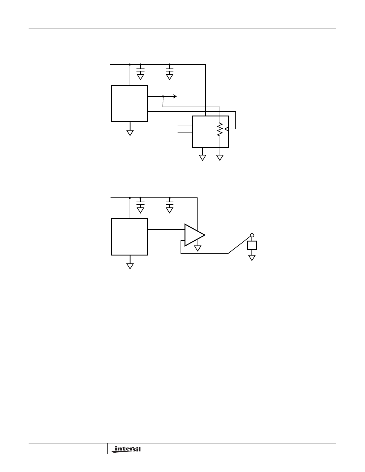
Output Voltage Adjustment
The output voltage can be adjusted up or down by 2.5% by
placing a potentiometer from Vout to ground, and connecting
the wiper to the TRIM pin. The TRIM input is high impedance,
so no series resistance is needed. The resistor in the
potentiometer should be a low tempco (<50ppm/°C) and the
resulting voltage divider should have very low tempco
<5ppm/°C. A digital potentiometer such as the ISL95810
provides a low tempco resistance and excellent resistor and
tempco matching for trim applications.
11
FN6326.1
April 12, 2007
Page 12

Typical Application Circuits
VIN = +5.0V
ISL21007
R = 200Ω
V
IN
2N2905
+2.7 to 5.5V
2-WIRE BUS
ISL21007
V
= 2.50V
OUT
GND
V
OUT
2.5V/50mA
0.001µF
FIGURE 29. PRECISION 2.5V 50mA REFERENCE
0.001µF
+
–
10µF
V
(UNBUFFERED)
EL8178
OUT
V
IN
ISL21007-25
V
= 2.50V
OUT
GND
V
SDA
SCL
V
OUT
CC
V
X9119
SS
0.1µF
R
H
R
L
V
OUT
(BUFFERED)
FIGURE 30. 2.5V FULL SCALE LOW-DRIFT, LOW NOISE, 10-BIT ADJUSTABLE VOLTAGE SOURCE
12
FN6326.1
April 12, 2007
Page 13
Typical Application Circuits
ISL21007
+2.7 to 5.5V
+2.7 to 5.5V
10µF
0.1µF
V
IN
V
ISL21007-12
TRIM
GND
OUT
2.5V ±2.5%
I2C BUS
V
SDA
SCL
ISL95810
V
SS
CC
R
H
R
L
FIGURE 31. OUTPUT ADJUSTMENT USING THE TRIM PIN
V
IN
V
ISL21007-12
GND
0.1µF
OUT
10µF
EL8178
+
–
V
OUT
SENSE
LOAD
FIGURE 32. KELVIN SENSED LOAD
13
FN6326.1
April 12, 2007
Page 14

Small Outline Plastic Packages (SOIC)
ISL21007
N
INDEX
AREA
123
-A-
E
-B-
SEATING PLANE
D
A
-C-
0.25(0.010) BM M
H
L
h x 45°
α
e
B
0.25(0.010) C AM BS
M
NOTES:
1. Symbols are defined in the “MO Series Symbol List” in Section 2.2 of
Publication Number 95.
2. Dimensioning and tolerancing per ANSI Y14.5M-1982.
3. Dimension “D” does not include mold flash, protrusions or gate burrs.
Mold flash, protrusion and gate burrs shall not exceed 0.15mm (0.006
inch) per side.
4. Dimension “E” does not include interlead flash or protrusions. Interlead flash and protrusions shall not exceed 0.25mm (0.010 inch) per
side.
5. The chamfer on the body is optional. If it is not present, a visual index
feature must be located within the crosshatched area.
6. “L” is the length of terminal for soldering to a substrate.
7. “N” is the number of terminal positions.
8. Terminal numbers are shown for reference only.
9. The lead width “B”, as measured 0.36mm (0.014 inch) or greater
above the seating plane, shall not exceed a maximum value of
0.61mm (0.024 inch).
10. Controlling dimension: MILLIMETER. Converted inch dimensions
are not necessarily exact.
A1
C
0.10(0.004)
M8.15 (JEDEC MS-012-AA ISSUE C)
8 LEAD NARROW BODY SMALL OUTLINE PLASTIC PACKAGE
INCHES MILLIMETERS
SYMBOL
A 0.0532 0.0688 1.35 1.75 -
A1 0.0040 0.0098 0.10 0.25 -
B 0.013 0.020 0.33 0.51 9
C 0.0075 0.0098 0.19 0.25 -
D 0.1890 0.1968 4.80 5.00 3
E 0.1497 0.1574 3.80 4.00 4
e 0.050 BSC 1.27 BSC -
H 0.2284 0.2440 5.80 6.20 -
h 0.0099 0.0196 0.25 0.50 5
L 0.016 0.050 0.40 1.27 6
N8 87
α
0° 8° 0° 8° -
NOTESMIN MAX MIN MAX
Rev. 1 6/05
All Intersil U.S. products are manufactured, assembled and tested utilizing ISO9000 quality systems.
Intersil Corporation’s quality certifications can be viewed at www.intersil.com/design/quality
Intersil products are sold by description only. Intersil Corporation reserves the right to make changes in circuit design, software and/or specifications at any time without
notice. Accordingly, the reader is cautioned to verify that data sheets are current before placing orders. Information furnished by Intersil is believed to be accurate and
reliable. However, no responsibility is assumed by Intersil or its subsidiaries for its use; nor for any infringements of patents or other rights of third parties which may result
from its use. No license is granted by implicat ion or oth erwise u nde r any p a tent or p at ent r ights of Intersil or its subsidiaries.
For information regarding Intersil Corporation and its products, see www.intersil.com
14
FN6326.1
April 12, 2007
 Loading...