

Page 1
查询ISL12029IV27AZ供应商
®
ISL1540
PRELIMINARY
Data Sheet February 21, 2006
-52V Dual Channel Differential DSL Line
Driver
The ISL1540 is a -52V dual channel differential amplifier
designed for driving full rate ADSL signals at very low power
dissipation. The high supply voltage allows operation from a
single standard -52V negative battery supply. It contains two
pairs of wideband, high voltage, current mode feedback
amplifiers optimized for lower power consumption and
highest performance in ADSL and ADSL2+ systems. The
line drivers have fixed gain A
= 48 with integrated feedback
V
and gain resistors. Its output clamping circuit eliminates the
requirement for the Zener protection diodes.
These drivers achieve an MTPR distortion measurement of
better than 70dB while consuming typically 3mA per DSL
channel of total supply current.
The ISL1540 is supplied in a thermally-enhanced 8mm x
8mm 32-pin QFN package and is specified for operating
over the full -40°C to +85°C temperature range.
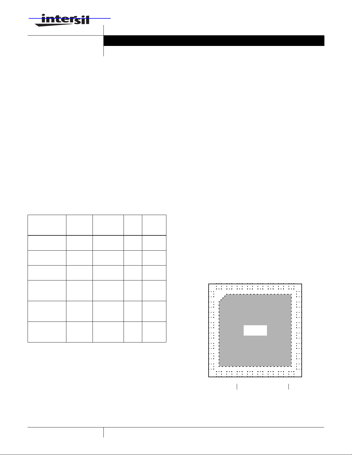
Ordering Information
TAPE
&
PART
NUMBER
ISL1540IR 1540IR 32-Pin QFN
ISL1540IR-T7 1540IR 32-Pin QFN
ISL1540IR-T13 1540IR 32-Pin QFN
ISL1540IRZ
(See Note)
ISL1540IRZ-T7
(See Note)
ISL1540IRZ-T13
(See Note)
NOTE: Intersil Pb-free plus anneal products employ special Pb-free
material sets; molding compounds/die attach materials and 100%
matte tin plate termination finish, which are RoHS compliant and
compatible with both SnPb and Pb-free soldering operations. Intersil
Pb-free products are MSL classified at Pb-free peak reflow
temperatures that meet or exceed the Pb-free requirements of
IPC/JEDEC J STD-020.
PART
MARKING PACKAGE
(8mm x 8mm)
(8mm x 8mm)
(8mm x 8mm)
1540IRZ 32-Pin QFN
(8mm x 8mm)
(Pb-Free)
1540IRZ 32-Pin QFN
(8mm x 8mm)
(Pb-Free)
1540IRZ 32-Pin QFN
(8mm x 8mm)
(Pb-Free)
REEL
13” MDP0046
13” MDP0046
PKG.
DWG. #
- MDP0046
7” MDP0046
- MDP0046
7” MDP0046
FN6113.0
Features
• 200mA output current driving capability
• Operates from a single -40V to -60V power supply
• 800mW per channel total power dissipation
• MTPR of -70dB
•96V
differential output swing
P-P
• Fixed gain, integrated gain resistors
• Current control pins
• Output clamp for lightning and surge protection
• Channel separation
-75dB @ 1MHz
• Pb-free plus anneal available (RoHS compliant)
Applications
• Dual port ADSL and ADSL2+ line drivers
• HDSL, HDSL2, HDSL 4 and SHDSL line drivers
• DSLAM, DLC, MDU/MTU line drivers
• Performance upgrade to Le87213 and Le87213A
Pinout
ISL1540
[32-PIN QFN (8mm x 8mm)]
TOP VIEW
OUTA
VBAT
GND
OUTB
NC
OUTC
NC
32
31
30
29
28
15 26
16ENCD 25 NC
MONCD
24
23
22
21
20
19
18
17
NC
NC
NC
NC
NC
INA
INB
NC
1
2
3
4
5
6
7
8
9
NC
10
11
AB
EN
MONAB
THERMAL
PAD
12
NC
13
GND
14 27
VCC
OUTD
NC
NC
NC
NC
NC
IND
INC
1
CAUTION: These devices are sensitive to electrostatic discharge; follow proper IC Handling Procedures.
1-888-INTERSIL or 321-724-7143
| Intersil (and design) is a registered trademark of Intersil Americas Inc.
All other trademarks mentioned are the property of their respective owners.
Copyright © Intersil Americas Inc. 2006. All Rights Reserved.
Page 2
ISL1540
Absolute Maximum Ratings (T
V
Voltage to GND . . . . . . . . . . . . . . . . . . . . . . . . . . -0.3V to 6.0V
CC
V
Voltage to GND. . . . . . . . . . . . . . . . . . . . . . . . . . . -65V to 0.3V
BAT
Driver V
+ Voltage . . . . . . . . . . . . . . . . . . . . . . . . . . . V
IN
ENA Voltage to GND . . . . . . . . . . . . . . . . . . . . . . . . . . -0.3V to V
I
Voltage to GND . . . . . . . . . . . . . . . . . . . . . . . . -0.3V to VCC-2V
ADJ
CAUTION: Stresses above those listed in “Absolute Maximum Ratings” may cause permanent damage to the device. This is a stress only rating and operation of the
device at these or any other conditions above those indicated in the operational sections of this specification is not implied.
IMPORTANT NOTE: All parameters having Min/Max specifications are guaranteed. Typical values are for information purposes only. Unless otherwise noted, all tests
are at the specified temperature and are pulsed tests, therefore: T
Electrical Specifications V
= 25°C)
A
to 0.0V
BAT
CC
= TC = T
J
= -52V, RF = 10kΩ, RL = 300Ω, VCC = 3.3V, I
BAT
A.
Current into any Input . . . . . . . . . . . . . . . . . . . . . . . . . . . . . . . . 8mA
Output Current from Driver (Static) . . . . . . . . . . . . . . . . . . . . . 50mA
Power Dissipation . . . . . . . . . . . . . . . . . . . . . . . . . . . . . See Curves
Storage Temperature Range . . . . . . . . . . . . . . . . . .-65°C to +150°C
Operating Temperature Range . . . . . . . . . . . . . . . . . -40°C to +85°C
Operating Junction Temperature . . . . . . . . . . . . . . .-40°C to +150°C
= EN = 0V, TA = 25°C. Amplifiers tested separately.
ADJ
PARAMETER DESCRIPTION CONDITIONS MIN TYP MAX UNIT
SUPPLY CHARACTERISTICS
I
(Full IS) Negative Supply Current per Amplifier All outputs at 0V, EN = 0V -3 mA
BAT
I
(Power-down) Negative Supply Current per Amplifier All outputs at 0V, EN = 3.3V 50 µA
BAT
INPUT CHARACTERISTICS
V
∆V
OS
OS
Input Offset Voltage -50 +10 +50 mV
VOS Mismatch -5 1 +5 mV
IB+ Non-Inverting Input Bias Current -15 +14 µA
I
- Inverting Input Bias Current -30 +30 µA
B
∆I
-I
B
R
OL
e
N
i
N
V
IH
V
IL
I
IH1
I
IH0
I
IL
- Mismatch -25 0 +25 µA
B
Transimpedance TBD TBD TBD MΩ
Input Noise Voltage TBD nV/√Hz
-Input Noise Current TBD pA/√Hz
Input High Voltage EN & MON inputs, with signal 2 V
Input Low Voltage EN & MON inputs 0.8 V
Input High Current for MON MON = 3.3V 0.05 0.25 5 µA
Input High Current for EN EN = 3.3V 0.05 0.5 5 µA
Input Low Current for C0 or MON EN = 0V, MON = 0V -0.3 0 +0.3 µA
OUTPUT CHARACTERISTICS
V
OUT-Headroom
I
OL
I
OUT
Loaded Output Headroom
(R
Single-ended to GND)
L
V
- V
BAT
OUT
RL = 300Ω 1.5 V
R
= 100Ω (+) 2.3 V
L
R
= 100Ω (-) 3.4 V
L
Linear Output Current AV = 5, RL = 100Ω, f = 100kHz,
THD = -60dBc (10Ω single-ended)
Output Current V
= 1V, RL = 1Ω 1A
OUT
200 mA
DYNAMIC PERFORMANCE
A
V
BW -3dB Bandwidth A
HD2 2nd Harmonic Distortion f
HD3 3rd Harmonic Distortion f
Gain 25kHz to 4MHz 48 V/V
= +48 14 MHz
V
= 1MHz, RL = 300Ω, V
C
f
= 1MHz, RL = 100Ω, V
C
= 1MHz, RL = 300Ω, V
C
= 1MHz, RL = 100Ω, V
f
C
OUT
OUT
OUT
OUT
= 2V
= 2V
= 2V
= 2V
P-P
P-P
P-P
P-P
TBD dBc
TBD dBc
TBD dBc
TBD dBc
2
FN6113.0
February 21, 2006
Page 3
ISL1540
Electrical Specifications V
PARAMETER DESCRIPTION CONDITIONS MIN TYP MAX UNIT
MTPR Multi-Tone Power Ratio 26kHz to 1.1MHz, R
SR Slewrate (single-ended) V
= -52V, RF = 10kΩ, RL = 300Ω, VCC = 3.3V, I
BAT
P
= 20.4dBM
LINE
from -24V to +24V measured at ±12V 750 V/µs
OUT
= EN = 0V, TA = 25°C. Amplifiers tested separately.
ADJ
LINE
= 600Ω,
-70 dBc
Pin Descriptions
PIN NUMBER PIN NAME PIN DESCRIPTION
1, 2, 3, 4, 5, 8, 9, 12, 19, 20,
21, 22, 23, 25, 26, 28
6 INA Input A
7 INB Input B
10 MONAB Full bias/half bias current control for AB amps
11 EN
13, 30 GND Ground
14 VCC 3.3V supply for bias and logic
15 MONCD Full bias/half bias current control for CD amps
16 EN
17 INC Input C
18 IND Input D
24 OUTD Output D
27 OUTC Output C
29 OUTB Output B
31 VBAT -52 battery voltage
32 OUTA Output A
NC Not connected
AB Enable/disable for AB amps
CD Enable/disable for CD amps
3
FN6113.0
February 21, 2006
Page 4

Block Diagram
ISL1540
INA
VBAT/2
INB
INC
VBAT/2
IND
10K
10K
10K
10K
LOGIC
CONTROL
AB
EN
MONAB
425
425
+
A
10K
10K
-
B
+
+
C
10K
10K
-
D
+
CONTROL
LOGIC
CD
EN
MONCD
OUTA
OUTB
OUTC
OUTD
4
FN6113.0
February 21, 2006
Page 5

Typical Performance Curves
ISL1540
VCC= +3.3V
= -52V
V
BAT
= +48
A
V
RL=1kΩ
RL=200Ω
FIGURE 1. FREQUENCY RESPONSE FOR VARIOUS R
VCC=+3.3V
=-50V
V
BAT
=500Ω
R
L
3rd HD
VCC= +3.3V
V
= -52V
BAT
=500Ω
R
L
CL=15pF
L
FIGURE 2. FREQUENCY RESPONSE FOR VARIOUS C
(EACH OUTPUTS TO GROUND)
VCC=+3.3V
=-50V
V
BAT
=500Ω
R
L
3rd HD
CL=39pF
CL=22pF
L
2nd HD
FIGURE 3. 1MHz 2nd & 3rd HARMONIC DISTORTION vs
OUTPUT VOLTAGE
VCC=+3.3V
=-50V
V
BAT
=500Ω
R
L
3rd HD
2nd HD
FIGURE 5. 3.75MHz 2nd & 3rd HARMONIC DISTORTION vs
OUTPUT VOLTAGE
2nd HD
FIGURE 4. 2.2MHz 2nd & 3rd HARMONIC DISTORTION vs
OUPUT VOLTAGE
VCC=+3.3V
=-50V
V
BAT
=500Ω
R
L
3.75 MHz
2.2 MHz
1MHz
FIGURE 6. TOTAL HARMONIC DISTORTION FOR VARIOUS
FREQUENCIES
5
FN6113.0
February 21, 2006
Page 6

Typical Performance Curves (Continued)
ISL1540
VCC=+3.3V
= -52V
V
BAT
AB ==> CD
CD ==> AB
VCC=+3.3V
V
= -25V
BAT
V
CC
FIGURE 7. CROSSTALK vs FREQUENCY FIGURE 8. PSRR vs FREQUENCY
JEDEC JESD51-7 HIGH EFFECTIVE
JEDEC JESD51-3 LOW EFFECTIVE
THERMAL CONDUCTIVITY TEST BOARD
1.2
947mW
1
0.8
0.6
0.4
0.2
POWER DISSIPATION (W)
0
0 255075100 150
AMBIENT TEMPERATURE (°C)
QFN32
θJA=132°C/W
12585
THERMAL CONDUCTIVITY TEST BOARD LPP EXPOSED DIEPAD SOLDERED TO
PCB PER JESD51-5
4.5
3.571W
4
3.5
3
2.5
2
1.5
1
POWER DISSIPATION (W)
0.5
0
0 255075100 150
AMBIENT TEMPERATURE (°C)
QFN32
θJA=35°C/W
12585
FIGURE 9. PACKAGE POWER DISSIPATION vs AMBIENT
TEMPERATURE
6
FIGURE 10. PACKAGE POWER DISSIPATION vs AMBIENT
TEMPERATURE
FN6113.0
February 21, 2006
Page 7

Application Information
PCB Layout Considerations for QFN Package
The ISL1540 die is packaged in a thermally efficient 32-pins
QFN leadless plastic package (8mm x 8mm). A thermal pad
is underneath the package and can use PCB surface metal
vias areas and internal ground planes to spread heat away
from the package. The larger the PCB area, the lower the
junction temperature of the device will be. In ADSL
applications, multiple layer circuit boards with internal
ground plane are generally used. 13 mil vias are
recommended to connect the metal area under the device
with internal ground plane.
Power Control Function
The ISL1540 contains four forms of power control operation.
The two inputs, MON1 and MON2, can be used to control
the supply current of the ISL1540 drive amplifiers. ENAB
and ENCD can be used to enable and disable the device.
Below is the table showing the power modes.
TABLE 1. POWER MODES FOR ISL1541
MON1 MON2 ENAB ENCD OPERATION
000 0I
1 1 0 0 1/2-IS Power Mode
X X 1 1 Power Down
Full Power Mode
S
ISL1540
7
FN6113.0
February 21, 2006
Page 8

Package Outline Drawing
ISL1540
All Intersil U.S. products are manufactured, assembled and tested utilizing ISO9000 quality systems.
Intersil Corporation’s quality certifications can be viewed at www.intersil.com/design/quality
Intersil products are sold by description only. Intersil Corporation reserves the right to make changes in circuit design, software and/or specifications at any time without
notice. Accordingly, the reader is cautioned to verify that data sheets are current before placing orders. Information furnished by Intersil is believed to be accurate and
reliable. However, no responsibility is assumed by Intersil or its subsidiaries for its use; nor for any infringements of patents or other rights of third parties which may result
from its use. No license is granted by implication or otherwise under any patent or patent rights of Intersil or its subsidiaries.
For information regarding Intersil Corporation and its products, see www.intersil.com
8
FN6113.0
February 21, 2006
 Loading...