

®
ISL1539
Data Sheet February 12, 2007
Dual Channel Differential VDSL2 Line
Driver
The ISL1539 is to be used for high performance long reach
and high speed applications, including ADSL2, ADSL2+, and
VDSL2 20dBm.
The ISL1539 is an integral part of the signal chain. The
driver has been optimized for flat gain response and reduced
harmonic distortion and noise in the bands of interest to
improve the overall signal to noise in the system.
These drivers achieve a total harmonic distortion (THD)
measurement of typically -60dB MTPR @ 1.1MHz, while
consuming typically 10mA per DSL channel of total supply
current. This supply current can be set using a resistor on
the I
adjust supply current to one of four pre-set modes (full-I
3/4-I
on ±5V to ±15V supplies and retains its bandwidth and
linearity over the complete supply range.
The device is supplied in the small fo otpri nt (4mmx5mm)
24 Ld QFN package and is specified for operation over the full
-40°C to +85°C temperature range.
pin. Two other pins (C0 and C1) can also be used to
ADJ
, 1/2-IS, and full power-down). The ISL1539 operates
S
,
S
FN7516.2
Features
• 450mA output drive capability
•44.1V
• -85dBc THD @ 1MHz 2V
differential output drive into 100Ω
P-P
P-P
• High slew rate of 1200V/µs differential
• Bandwidth - 80MHz @ A
= 10
V
• Current control pins
• Channel separation
- 80dB @ 500kHz
-75dB @ 1MHz
-60dB @ 4MHz
• Pb-free plus anneal available (RoHS compliant)
Applications
• VDSL2 20dBm
•ADSL2++
Pinouts
VS-
C0AB
C1AB
VINA+
VINB+
GND
IADJ
VINC+
VIND+
C1CD
C0CD
VS-
1
2
3
4
5
6
7
8
9
10
11
12
ISL1539
(24 LD HTSSOP)
TOP VIEW
THERMAL
PAD
24
23
22
21
20
19
18
17
16
15
14
13
VS+
VOUTA
VINA-
VINB-
VOUTB
NC
NC
VOUTC
VINC-
VIND-
VOUTD
VS+
VINA+
VINB+
GND
IADJ
NC
VINC+
VIND+
1
2
3
4
5
6
7
ISL1539
(24 LD QFN)
TOP VIEW
C1AB
C0AB
24
23
THERMAL
PAD
8
9
C1CD
C0CD
VS-
VS+
VOUTA
22
21
20
19
VINA-
18
VINB-
17
VOUTB
16
NC/SHIELD
15
VOUTC
14
VINC-
13
VIND-
10
11
12
VS-
VS+
VOUTD
1
CAUTION: These devices are sensitive to electrostatic discharge; follow proper IC Handling Procedures.
1-888-INTERSIL or 1-888-468-3774
| Intersil (and design) is a registered trademark of Intersil Americas Inc.
Copyright © Intersil Americas Inc. 2006-2007. All Rights Reserved.
All other trademarks mentioned are the property of their respective owners.
Ordering Information
ISL1539
PART NUMBER
(Note) PART MARKING TAPE & REEL
ISL1539IRZ 1539 IRZ - 24 Ld QFN MDP0046
ISL1539IRZ-T7 1539 IRZ 7” 24 Ld QFN MDP0046
ISL1539IRZ-T13 1539 IRZ 13” 24 Ld QFN MDP0046
ISL1539IVEZ 1539 IVEZ - 24 Ld HTSSOP MDP0048
ISL1539IVEZ-T7 1539 IVEZ 7” 24 Ld HTSSOP MDP0048
ISL1539IVEZ-T13 1539 IVEZ 13” 24 Ld HTSSOP MDP0048
NOTE: Intersil Pb-free plus anneal products employ special Pb-free material sets; molding compounds/die attach materials and 100% matte tin plate
termination finish, which are RoHS compliant and compatible with both SnPb and Pb-free soldering operations. Intersil Pb-free products are MSL
classified at Pb-free peak reflow temperatures that meet or exceed the Pb-free requirements of IPC/JEDEC J STD-020.
PACKAGE
(Pb-free) PKG. DWG. #
2
FN7516.2
February 12, 2007
ISL1539
Absolute Maximum Ratings (T
V
+ to VS- Supply Voltage. . . . . . . . . . . . . . . . . . . . . .-0.3V to +30V
S
V
+ Voltage to GND . . . . . . . . . . . . . . . . . . . . . . . . . .-0.3V to +30V
S
V
- Voltage to GND. . . . . . . . . . . . . . . . . . . . . . . . . . .-30V to +0.3V
S
Driver V
C
0
I
ADJ
+ Voltage . . . . . . . . . . . . . . . . . . . . . . . . . . . . . VS- to VS+
IN
, C1 Voltage to GND . . . . . . . . . . . . . . . . . . . . . . . . .-0.3V to +6V
Voltage to GND . . . . . . . . . . . . . . . . . . . . . . . . . . .-0.3V to +4V
= +25°C)
A
Current into any Input . . . . . . . . . . . . . . . . . . . . . . . . . . . . . . . . 8mA
Output Current from Driver (Static) . . . . . . . . . . . . . . . . . . . . . 50mA
Power Dissipation . . . . . . . . . . . . . . . . . . . . . . . . . . . . . See Curves
Storage Temperature Range . . . . . . . . . . . . . . . . . .-65°C to +150°C
Operating Temperature Range . . . . . . . . . . . . . . . . .-40°C to +85°C
Operating Junction Temperature . . . . . . . . . . . . . . .-40°C to +150°C
ESD Rating
Human Body Model (Per MIL-STD-883 Method 3015.7). . . . .3kV
Machine Model (Per EIAJ ED-4701 Method C-111). . . . . . . .250V
CAUTION: Stresses above those listed in “Absolute Maximum Ratings” may cause permanent damage to the device. This is a stress only rating and operation of the
device at these or any other conditions above those indicated in the operational sections of this specification is not implied.
IMPORT ANT NOTE: A ll p arameters having Min/Max specificati ons are gua ranteed. Typ values are for information purposes only. Unless otherwise n oted, all test s ar e at
the specified temperature and are pulsed tests, theref ore: T
Electrical Specifications V
= ±12V, RF = 3kΩ, RL= 65Ω, I
S
= TC = T
J
A
= C0 = C1 = 0V, TA = +25°C. Amplifiers tested separately.
ADJ
PARAMETER DESCRIPTION CONDITIONS MIN TYP MAX UNIT
SUPPLY CHARACTERISTICS
I
+ (Full IS) Positive Supply Current per Amplifier All outputs at 0V, C0 = C1 = 0V, R
S
I
- (Full IS) Negative Supply Current per Amplifier All outputs at 0V, C0 = C1 = 0V, R
S
IS+ (3/4 IS) Positive Supply Current per Amplifier All outputs at 0V, C0 = 5V, C1 = 0V, R
I
- (3/4 IS) Negative Supply Current per Amplifier All outputs at 0V, C0 = 5V, C1 = 0V, R
S
I
+ (1/2 IS) Positive Supply Current per Amplifier All outputs at 0V, C0 = 0V, C1 = 5V, R
S
I
- (1/2 IS) Negative Supply Current per Amplifier All outputs at 0V, C0 = 0V, C1 = 5V, R
S
IS+ (Power-down) Positive Supply Current per Amplifier All outputs at 0V, C0 = C1 = 5V, R
I
- (Power-down) Negative Supply Current per Amplifier All outputs at 0V, C0 = C1 = 5V, R
S
I
GND
GND Supply Current per Amplifier All outputs at 0V 0.1 mA
= 0 7.5 10 12.5 mA
ADJ
= 0 -12.4 -9.9 -7.4 mA
ADJ
= 0 7.5 mA
ADJ
= 0 -7.4 mA
ADJ
= 0 3.7 5.1 6.3 mA
ADJ
= 0-6.2-5-3.5mA
ADJ
= 0 0.1 0.25 mA
ADJ
= 0 -0.25 0 mA
ADJ
INPUT CHARACTERISTICS
V
ΔV
OS
OS
Input Offset Voltage -2 +1 +2 mV
VOS Mismatch -5 0 +5 mV
IB+ Non-Inverting Input Bias Current -10 +10 µA
I
- Inverting Input Bias Current -75 +60 µA
B
ΔI
-I
B
R
OL
e
N
i
N
V
IH
V
IL
I
IH0 , IIH1
I
IL0, IIL1
- Mismatch -15 0 +15 µA
B
Transimpedance 3MΩ
Input Noise Voltage 2.7 nV/√Hz
-Input Noise Current 19 pA/√Hz
Input High Voltage C0 and C1 inputs, with signal 1.8 V
C
and C1 inputs, without signal 1.6 V
0
Input Low Voltage C0 and C1 inputs 0.8 V
Input High Current for C
0, C1
Input Low Current for C0 or C
1
C0 = 5V, C1 = 5V 10 40 µA
C0 = 0V, C1 = 0V -15 -4.0 µA
3
FN7516.2
February 12, 2007
V
V
ISL1539
Electrical Specifications V
= ±12V, RF = 3kΩ, RL= 65Ω, I
S
= C0 = C1 = 0V, TA = +25°C. Amplifiers tested separately. (Continued)
ADJ
PARAMETER DESCRIPTION CONDITIONS MIN TYP MAX UNIT
OUTPUT CHARACTERISTICS
V
OUT
Loaded Output Swing
(R
Single-ended to GND)
L
= 100Ω ±11.1 V
R
L
= 50Ω (+) 10.65 10.95 V
R
L
R
= 50Ω (-) -10.95 -10.55 V
L
R
= 25Ω (+) 9.8 10.7 V
L
RL = 25Ω (-) -10.7 -9.2 V
I
OL
Linear Output Current AV = 5, RL = 10Ω, f = 100kHz, THD = -60dBc
450 mA
(10Ω single-ended)
I
OUT
Output Current V
= 1V, RL = 1Ω 1A
OUT
DYNAMIC PERFORMANCE
BW -3dB Bandwidth A
HD2 at 200kHz 2nd Harmonic Distortion at 200kHz fC = 200kHz, RL = 100Ω, V
HD3 at 200kHz 3rd Harmonic Distortion at 200kHz f
THD at 200kHz Total Harmonic Distortion at 200kHz f
HD2 at 1MHz 2nd Harmonic Distortion at 1MHz fC = 1MHz, RL = 100Ω, V
HD3 at 1MHz 3rd Harmonic Distortion at 1MHz f
THD at 1MHz Total Harmonic Distortion at 1MHz fC = 1MHz, RL = 100Ω, V
MTPR Multi-Tone Power Ratio 26kHz to 1.1MHz, R
SR Slewrate ( single-ended) V
= +10 80 MHz
V
= 2V
OUT
= 200kHz, RL = 100Ω, V
C
= 200kHz, RL = 100Ω, V
C
f
= 1MHz, RL = 25Ω, V
C
= 1MHz, RL = 100Ω, V
C
f
= 1MHz, RL = 25Ω, V
C
P
= 20.4dBM
LINE
from -8V to +8V measured at ±4V 500 V/µs
OUT
LINE
OUT
OUT
OUT
OUT
OUT
OUT
OUT
= 100Ω,
= 2V
= 2V
= 2V
= 2V
= 2V
= 2V
= 2V
P-P
P-P
P-P
P-P
P-P
P-P
P-P
P-P
-90 dBc
-94 dBc
-89 dBc
-86 dBc
-80 dBc
-90 dBc
-75 dBc
-85 dBc
-70 dBc
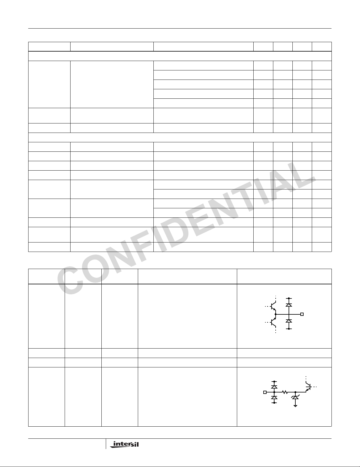
Pin Descriptions
ISL1539IR
(QFN24)
1 4 VINA+ Amplifier A non-inverting input
2 5 VINB+ Amplifier B non-inverting input (Reference Circuit 1)
3 6 GND Ground connection
4 7 IADJ (Note 1) Supply current control pin for both DSL
ISL1539IVE
(HTSSOP24) PIN NAME FUNCTION CIRCUIT
channels #1 and #2
I
ADJ
CIRCUIT 1
+
S
VS-
CIRCUIT 2
+
S
-
V
S
GND
4
FN7516.2
February 12, 2007

Pin Descriptions (Continued)
V
V
ISL1539
ISL1539IR
(QFN24)
ISL1539IVE
(HTSSOP24) PIN NAME FUNCTION CIRCUIT
5 18, 19 NC Not connected
6 8 VINC+ Amplifier C non-inverting input (Reference Circuit 1)
7 9 VIND+ Amplifier D non-inverting input (Reference Circuit 1)
8 10 C1CD (Note 2) DSL channel #2 current control pin
9 11 C0CD (Note 2) DSL channel #2 current control pin (Reference Circuit 3)
10, 22 1, 12 VS- Negative supply
11, 21 13, 24 VS+ Positive supply
12 14 VOUTD Amplifier D output (Reference Circuit 1)
13 15 VIND- Amplifier D inverting input (Reference Circuit 1)
14 16 VINC- Amplifier C inverting input (Reference Circuit 1)
15 17 VOUTC Amplifier C output (Reference Circuit 1)
16 NC/SHIELD
17 20 VOUTB Amplifier B output (Reference Circuit 1)
18 21 VINB- Amplifier B inverting input (Reference Circuit 1)
19 22 VINA- Amplifier A inverting input (Reference Circuit 1)
20 23 VOUTA Amplifier A output (Reference Circuit 1)
23 2 C0AB (Note 3) DSL channel #1 current control pin (Reference Circuit 3)
24 3 C1AB (Note 3) DSL channel #1 current control pin (Reference Circuit 3)
NOTES:
1. I
controls bias current (IS) setting for both DSL channels.
ADJ
2. Amplifiers C and D comprise DSL channel #2. C
3. Amplifiers A and B comprise DSL channel #1. C
0CD
0AB
and C
and C
control IS settings for DSL channel #2.
1CD
control IS settings for DSL channel #1.
1AB
I
ADJ
+
S
1K
CIRCUIT 3
+
S
C
OAB
V
-
S
5
FN7516.2
February 12, 2007

Typical Performance Curves
ISL1539
VS = ±12V
C
= 1.8pF
L
A
V
R
L
= +12.4
= 100Ω
RF = 5kΩ
RF = 2kΩ
RF = 3kΩ
FIGURE 1. FREQUENCY RESPONSE FOR VARIOUS RF
(FULL POWER MODE)
VS = ±12V
= 5kΩ
R
F
= +12.4
A
V
= 100Ω
R
L
CL = 100pF
CL = 47pF
CL = 22pF
CL = 1.8pF
VS = ±12V
= 1.8pF
C
L
A
V
R
L
= +12.4
= 100Ω
RF = 5kΩ
RF = 2kΩ
RF = 3kΩ
FIGURE 2. FREQUENCY RESPONSE FOR VARIOUS RF
(HALF POWER MODE)
VS = ±12V
A
= +12.4
C
R
V
= 27pF
L
= 100Ω
L
RF = 4.99kΩ
RF = 3.48kΩ
FIGURE 3. FREQUENCY RESPONSE FOR VARIOUS C
(FULL POWER MODE)
VS = ±12V
R
= 3kΩ
F
= +12.4
A
V
R
= 100Ω
L
2nd HD
3rd HD
L
FIGURE 5. 200KHz 2ND AND 3RD HARMONIC DISTORTION
vs VOLTAGE OUTPUT (FULL POWER MODE)
FIGURE 4. COMMON MODE FREQUENCY RESPONSE FOR
VARIOUS R
VS = ±12V
= 5kΩ
R
F
= +12.4
A
V
= 100Ω
R
L
(FULL POWER MODE)
F
2nd HD
3rd HD
FIGURE 6. 200kHz 2ND AND 3RD HARMONIC DISTORTION
vs VOLTAGE OUTPUT (HALF POWER MODE)
6
FN7516.2
February 12, 2007

Typical Performance Curves (Continued)
ISL1539
VS = ±12V
= 3kΩ
R
F
= +12.4
A
V
= 100Ω
R
L
2nd HD
3rd HD
FIGURE 7. 1MHz 2ND AND 3RD HARMONIC DISTORTION vs
OUTPUT VOLTAGE (FULL POWER MODE)
VS = ±12V
= 3kΩ
R
F
= +12.4
A
V
= 100Ω
R
L
3rd HD
VS = ±12V
= 5kΩ
R
F
A
= +12.4
V
= 100Ω
R
L
3rd HD
2nd HD
FIGURE 8. 1MHz 2ND AND 3RD HARMONIC DISTORTION vs
OUPUT VOLTAGE (HALF POWER MODE)
VS = ±12V
R
= 5kΩ
F
= +12.4
A
R
V
= 100Ω
L
3rd HD
2nd HD
FIGURE 9. 3.75MHz 2ND AND 3RD HARMONIC DISTORTION
vs OUTPUT VOLTAGE (FULL POWER MODE)
VS = ±12V
= 3kΩ
R
F
A
= +12.4
V
R
= 100Ω
L
3rd HD
2nd HD
FIGURE 11. 10MHz 2ND AND 3RD HARMONIC DISTORTION
vs OUTPUT VOLTAGE (FULL POWER MODE)
2nd HD
FIGURE 10. 3.75MHz 2ND AND 3RD HARMONIC DISTORTION
vs OUTPUT VOLTAGE (HALF POWER MODE)
VS = ±12V
R
= 3kΩ
F
= +12.4
A
V
= 100Ω
R
L
10MHz
3.75MHz
1MHz
200kHz
FIGURE 12. TOTAL HARMONIC DISTORTION FOR V ARIOUS
FREQUENCIES (FULL POWER MODE)
7
FN7516.2
February 12, 2007

Typical Performance Curves (Continued)
ISL1539
VS = ±12V
R
= 3kΩ
F
= +12.4
A
V
= 100Ω R
R
L
ADJ
R
= 475Ω
ADJ
= 0Ω
R
ADJ
= 2kΩ
FIGURE 13. FREQUENCY RESPONSE FOR VARIOUS R
0
-10
-20
-30
-40
-50
-60
-70
-80
CHANNEL SEPARATION (dB)
-90
-100
100k 1M 10M 100M
FREQUENCY (Hz)
AB =>CD
CD=>AB
ADJ
3/4 +I
(mA)
S
+/- I
1/2 +I
FIGURE 14. SUPPLY CURRENT vs R
POWER MODE
FULL +I
S
S
FULL -I
S
S
1/2 -I
3/4 -I
S
S
R
(Ω)
ADJ
ADJ
FIGURE 15. CHANNEL SEPARATION vs FREQUENCY FIGURE 16. TRANSIMPEDANCE
VS = ±12V
FOR V ARIOUS
JEDEC JESD51-7 HIGH EFFECTIVE
THERMAL CONDUCTIVITY TEST BOARD HTSSOP EXPOSED DIEPAD SOLDERED
VS = ±12V
= 1kΩ
R
L
PSRR-
PSRR+
TO PCB PER JESD51-5
4.5
4.0
3.5
3.0
2.5
2.0
1.5
1.0
POWER DISSIPATION (W)
0.5
0.0
0 255075100 150
3.788W
3.378W
QFN-24
θ
= +37°C/W
JA
AMBIENT TEMPERATURE (°C)
HTSSOP-24
θ
=+33°C/W
JA
12585
FIGURE 17. PSRR vs FREQUENCY FIGURE 18. PACKAGE POWER DISSIP A TION vs AMBIENT
TEMPERATURE
8
February 12, 2007
FN7516.2

Typical Performance Curves (Continued)
JEDEC JESD51-3 LOW EFFECTIVE
THERMAL CONDUCTIVITY TEST BOARD
1.2
1.0
0.8
893mW
0.6
0.4
0.2
POWER DISSIPATION (W)
0.0
0 255075100 150
QFN-24
θ
= +140°C/W
JA
AMBIENT TEMPERATURE (°C)
FIGURE 19. PACKAGE POWER DISSIPATION vs AMBIENT TEMPERATURE
Application Information
The ISL1539 consists of two sets of high-power line driver
amplifiers that can be connected for full duplex differential
line transmission. The amplifiers are designed to be used
with signals up to 30MHz and produce low distortion levels.
A typical interface circuit is shown in Figure 20 below.
ISL1539
1.042W
HTSSOP-24
θ
= +120°C/W
JA
12585
+
-
R
F
2R
G
R
F
DRIVER
INPUT
RECEIVE
OUT +
RECEIVE
OUT -
R
G
RECEIVE
AMPLIFIERS
R
R
OUT
OUT
+
-
R
F
R
F
-
+
R
R
F
-
R
+
IN
+
R
-
R
R
IN
F
LINE +
LINE -
Z
LINE
FIGURE 20. TYPICAL LINE INTERFACE CONNECTION
The amplifiers are wired with one in positive gain and the
other in a negative gain configuration to generate a
differential output for a single-ended input. They will exhibit
very similar frequency responses for gains of three or
greater and thus generate very small common-mode outputs
over frequency, but for low gains the two drivers RF's need
to be adjusted to give similar frequency responses. The
positive-gain driver will generally exhibit more bandwidth and
peaking than the negative-gain driver.
If a differential signal is available to the drive amplifiers, they
may be wired so:
-
+
FIGURE 21. DRIVERS WIRED FOR DIFFERENTIAL INPUT
Each amplifier has identical positive gain connections, and
optimum common-mode rejection occurs. Further, DC input
errors are duplicated and create common-mode rather than
differential line errors.
Power Supplies and Dissipation
Due to the high power drive capability of the ISL1539, much
attention needs to be paid to power dissipation. The power
that needs to be dissipated in the ISL1539 has two main
contributors. The first is the quiescent current dissipation.
The second is the dissipation of the output stage.
The quiescent power in the ISL1539 is not constant with
varying outputs. In reality, 7mA of the 15mA needed to
power the drivers is converted in to output current.
Therefore, in the equation below we should subtract the
average output current, I
We’ll call this term I
Therefore, we can determine a quiescent current with the
following equation:
P
DquiescentVSIS2IX
where:
•V
is the supply voltage (VS+ to VS-)
S
is the maximum quiescent supply current (IS+ + IS-)
•I
S
•I
is the lesser of IO or 7mA (generally IX = 7mA)
X
, or 7mA, whichever is the lowest.
O
.
X
–()×=
(EQ. 1)
9
FN7516.2
February 12, 2007
ISL1539
The dissipation in the output stage has two main
contributors. Firstly, we have the average voltage drop
across the output transistor and secondly, the average
output current. For minimal power dissipation, the user
should select the supply voltage and the line transformer
ratio accordingly. The supply voltage should be kept as low
as possible, while the transformer ratio should be selected
so that the peak voltage required from the ISL1539 is close
to the maximum available output swing. There is a trade off,
however, with the selection of transformer ratio. As the ratio
is increased, the receive signal available to the receivers is
reduced.
Once the user has selected the transformer rati o, the
dissipation in the output stages can be selected with the
following equation:
P
Dtransistors
=
2I
⎛
-------
×× V
O
⎝
⎞
–
O
⎠
2
(EQ. 2)
V
S
where:
•V
is the supply voltage (VS+ to VS-)
S
is the average output voltage per channel
•V
O
•I
is the average output current per channel
O
The overall power dissipation (P
P
Dquiescent
and P
Dtransistor
.
) is obtained by adding
DISS
Then, the θJA requirement needs to be calculated. This is
done using the following equation:
T
-------------------------------------------------
=
θ
JA
–()
JUNCTTAMB
P
DISS
(EQ. 3)
where:
•T
•T
•P
• θ
is the maximum die temperature (+150°C)
JUNCT
is the maximum ambient temperature
AMB
is the dissipation calculated above
DISS
is the junction to ambient thermal resistance for the
JA
package when mounted on the PCB
This θ
value is then used to calculate the area of copper
JA
needed on the board to dissipate the power.
The IRE and QFN power packages are designed so that
heat may be conducted away from the device in an efficient
manner. To disperse this heat, the bottom diepad is internally
connected to the mounting platform of the die. Heat flows
through the diepad into the circuit board copper, then
spreads and convects to air. Thus, the ground plane on the
component side of the board becomes the heatsink. This
has proven to be a very effective technique. θ
of +30°C/W
JA
can be achieved.
Single Supply Operation
The ISL1539 can also be powered from a single supply
voltage. When operating in this mode, the GND pins can still
be connected directly to GND. To calculate power
dissipation, the equations in the previous section should be
used, with V
equal to half the supply rail.
S
Output Loading
While the drive amplifiers can output in excess of 450mA
transiently, the internal metallization is not designed to carry
more than 75mA of steady DC current and there is no currentlimit mechanism. This allows safely driving rms sinusoidal
currents of 2mAx75mA, or 150mA. This current is more than
that required to drive line impedances to large output levels,
but output short circuits cannot be tolerated. The series output resistor will usually limit currents to safe values in the
event of line shorts. Driving lines with no series resistor is a
serious hazard.
Power Supplies
The power supplies should be well bypassed close to the
ISL1539. A 3.3µF tantalum capacitor for each supply works
well. Since the load currents are differential, they should not
travel through the board copper and set up ground loops that
can return to amplifier inputs. Due to the class AB output
stage design, these currents have heavy harmonic content.
If the ground terminal of the positive and negative bypass
capacitors are connected to each other directly and then
returned to circuit ground, no such ground loops will occur.
This scheme is employed in the layout of the EL1537
demonstration board, and documentation can be obtained
from the factory.
Power Control Function
The ISL1539 contains two forms of power control operation.
Two digital inputs, C
supply current of the ISL1539 drive amplifiers. As the supply
current is reduced, the ISL1539 will start to exhibit slightly
higher levels of distortion and the frequency response will be
limited. The four power modes of the ISL1539 are set up as
shown in the table below
C
1
00I
013/4-I
101/2-I
11Power Down
and C1, can be used to control the
0
.
POWER MODES OF THE EL1537
C
0
Full Power Mode
S
Power Mode
S
Power Mode
S
OPERATION
10
FN7516.2
February 12, 2007

ISL1539
QFN (Quad Flat No-Lead) Package Family
A
1
2
3
2X
0.075 C
L
(E2)
C
SEATING
PLANE
0.08 C
N LEADS
& EXPOSED PAD
A
C
N
(N-1)
PIN #1
I.D. MARK
TOP VIEW
0.10 BAMC
b
N LEADS
(N/2)
BOTTOM VIEW
e
SIDE VIEW
(c)
A1
DETAIL X
D
(N-2)
(N/2)
(N-2)
(N-1)
N
(D2)
0.10
SEE DETAI L "X"
2
N LEADS
(L)
0.075
PIN #1 I.D.
1
2
3
NE
7
C
2X
B
E
C
3
5
MDP0046
QFN (QUAD FLAT NO-LEAD) PACKAGE FAMILY
(COMPLIANT TO JEDEC MO-220)
SYMBOL QFN44 QFN38 QFN32 TOLERANCE NOTES
A 0.90 0.90 0.90 0.90 ±0.10 -
A1 0.02 0.02 0.02 0.02 +0.03/-0.02 -
b 0.25 0.25 0.23 0.22 ±0.02 c 0.20 0.20 0.20 0.20 Reference D 7.00 5.00 8.00 5.00 Basic -
D2 5.10 3.80 5.80 3.60/2.48 Reference 8
E 7.00 7.00 8.00 6.00 Basic -
E2 5.10 5.80 5.80 4.60/3.40 Reference 8
e 0.50 0.50 0.80 0.50 Basic L 0.55 0.40 0.53 0.50 ±0.05 -
N 44 38 32 32 Reference 4
ND 11 7 8 7 Reference 6
NE 11 12 8 9 Reference 5
TOLER-
SYMBOL QFN28 QFN24 QFN20 QFN16
A 0.90 0.90 0.90 0.90 0.90 ±0.10 -
A1 0.02 0.02 0.02 0.02 0.02 +0.03/
b 0.25 0.25 0.30 0.25 0.33 ±0.02 -
c 0.20 0.20 0.20 0.20 0.20 Reference -
D 4.00 4.00 5.00 4.00 4.00 Basic D2 2.65 2.80 3.70 2.70 2.40 Reference -
E 5.00 5.00 5.00 4.00 4.00 Basic -
E2 3.65 3.80 3.70 2.70 2.40 Reference -
e 0.50 0.50 0.65 0.50 0.65 Basic -
L 0.40 0.40 0.40 0.40 0.60 ±0.05 -
N 28 24 20 20 16 Reference 4
ND 6 5 5 5 4 Reference 6
NE 8 7 5 5 4 Reference 5
NOTES:
1. Dimensioning and tolerancing per ASME Y14.5M-1994.
2. Tiebar view shown is a non-functional feature.
3. Bottom-side pin #1 I.D. is a diepad chamfer as shown.
4. N is the total number of terminals on the device.
5. NE is the number of terminals on the “E” side of the package
(or Y-direction).
6. ND is the number of terminals on the “D” side of the package
(or X-direction). ND = (N/2)-NE.
7. Inward end of terminal may be square or circular in shape with radius
(b/2) as shown.
8. If two values are listed, multiple exposed pad options are available.
Refer to device-specific datasheet.
ANCE NOTES
-
-0.02
Rev 10 12/04
11
FN7516.2
February 12, 2007

HTSSOP (Heat-Sink TSSOP) Family
ISL1539
0.25 CABM
E
E1
B
EXPOSED
THERMAL PAD
C
SEATING
PLANE
0.10 C
N LEADS
N
1
TOP VIEW
e
b
SIDE VIEW
(N/2)+1
(N/2)
D1
BOTTOM VIEW
0.10 CAB
AD
PIN #1 I.D.
N/2 LEAD TIPS
0.05
M
0.20 C2XB A
E2
H
MDP0048
HTSSOP (Heat-Sink TSSOP) Family
SYMBOL 14 LD 20 LD 24 LD 28 LD 38 LD TOLERANCE
A 1.20 1.20 1.20 1.20 1.20 Max
A1 0.075 0.075 0.075 0.075 0.075 ±0.075
A2 0.90 0.90 0.90 0.90 0.90 +0.15/-0.10
b 0.25 0.25 0.25 0.25 0.22 +0.05/-0.06
c 0.15 0.15 0.15 0.15 0.15 +0.05/-0.06
D 5.00 6.50 7.80 9.70 9.70 ±0.10
D1 3.2 4.2 4.3 5.0 7.25 Reference
E 6.40 6.40 6.40 6.40 6.40 Basic
E1 4.40 4.40 4.40 4.40 4.40 ±0.10
E2 3.0 3.0 3.0 3.0 3.0 Reference
e 0.65 0.65 0.65 0.65 0.50 Basic
L 0.60 0.60 0.60 0.60 0.60 ±0.15
L1 1.00 1.00 1.00 1.00 1.00 Reference
N 1420242838Reference
Rev. 2 12/03
NOTES:
1. Dimension “D” does not include mold flash, protrusions or gate
burrs. Mold flash, protrusions or gate burrs shall not exceed
0.15mm per side.
2. Dimension “E1” does not include interlead flash or protrusions.
Interlead flash and protrusions shall not exceed 0.25mm per
side.
3. Dimensions “D” and “E1” are measured at Datum Plane H.
4. Dimensioning and tolerancing per ASME Y14.5M-1994.
SEE DETAIL “X”
END VIEW
L1
A2
A
A1
DETAIL X
L
0° - 8°
GAUGE
PLANE
c
0.25
All Intersil U.S. products are manufactured, assembled and tested utilizing ISO9000 quality systems.
Intersil Corporation’s quality certifications can be viewed at www.intersil.com/design/quality
Intersil products are sold by description only. Intersil Corporation reserves the right to make changes in circuit design, software and/or specifications at any time without
notice. Accordingly, the reader is cautioned to verify that data sheets are current before placing orders. Information furnished by Intersil is believed to be accurate and
reliable. However, no responsibility is assumed by Intersil or its subsidiaries for its use; nor for any infringements of patents or other rights of third parties which may result
from its use. No license is granted by implicat ion or oth erwise u nde r any p a tent or p at ent r ights of Intersil or its subsidiaries.
For information regarding Intersil Corporation and its products, see www.intersil.com
12
FN7516.2
February 12, 2007
 Loading...