

®
ISL14010, ISL14017
Data Sheet April 16, 2007
Low Jitter Clock Generators for Set-Top
Box
The ISL14010 series of devices are general purpose
integrated Clock Synthesizers and Generators suited for
consumer applications such as Set-top Box, and various
other consumer applications.
The selectable reference input accepts 30MHz signal either
from crystal or an external source. It is specified to operate
with a nominal 3.3V supply and is offered in 16 Ld QFN
package.
Contact Factory for other output frequency options
.
Ordering Information
PART
NUMBER
ISL14010IRZ* 10IZ -40 to +85 16 LD QFN L16.3x3
ISL14017IRZ* 17IZ -40 to +85 16 LD QFN L16.3x3
*Add "-T" suffix for tape and reel.
NOTE: Intersil Pb-free plus anneal products employ special Pb-free
material sets; molding compounds/die attach materials and 100% matte
tin plate termination finish, which are RoHS compliant and compatible
with both SnPb and Pb-free soldering operations. Intersil Pb-free
products are MSL classified at Pb-free peak reflow temperatures that
meet or exceed the Pb-free requirements of IPC/JEDEC J STD-020.
PART
MARKING
TEMP.
RANGE (°C) PACKAGE
PKG.
DWG. #
Selection Table
PART
OPTIONS
ISL14010 30MHz 4 LVTTL 25, 30, 48, 54 16 LD QFN
ISL14017 30MHz 4 LVTTL 25, 30, 40, 50 16 LD QFN
INPUT
FREQUENCY
NUMBER OF
OUTPUTS
OUTPUT
FREQUENCY PACKAGE
FN6407.1
Features
• LVTTL Outputs
• Selectable Crystal or Ref. Clock for Inputs
• Period Jitter ~50ps RMS
• Single Supply; 3.3V nominal
• Extended Temperature Range: -40ºC to +85ºC
• Available in small foot print package
- 16 Ld QFN 3mmx3mm
• Pb-Free plus anneal available (RoHS Compliant)
Applications
• Set-Top Boxes
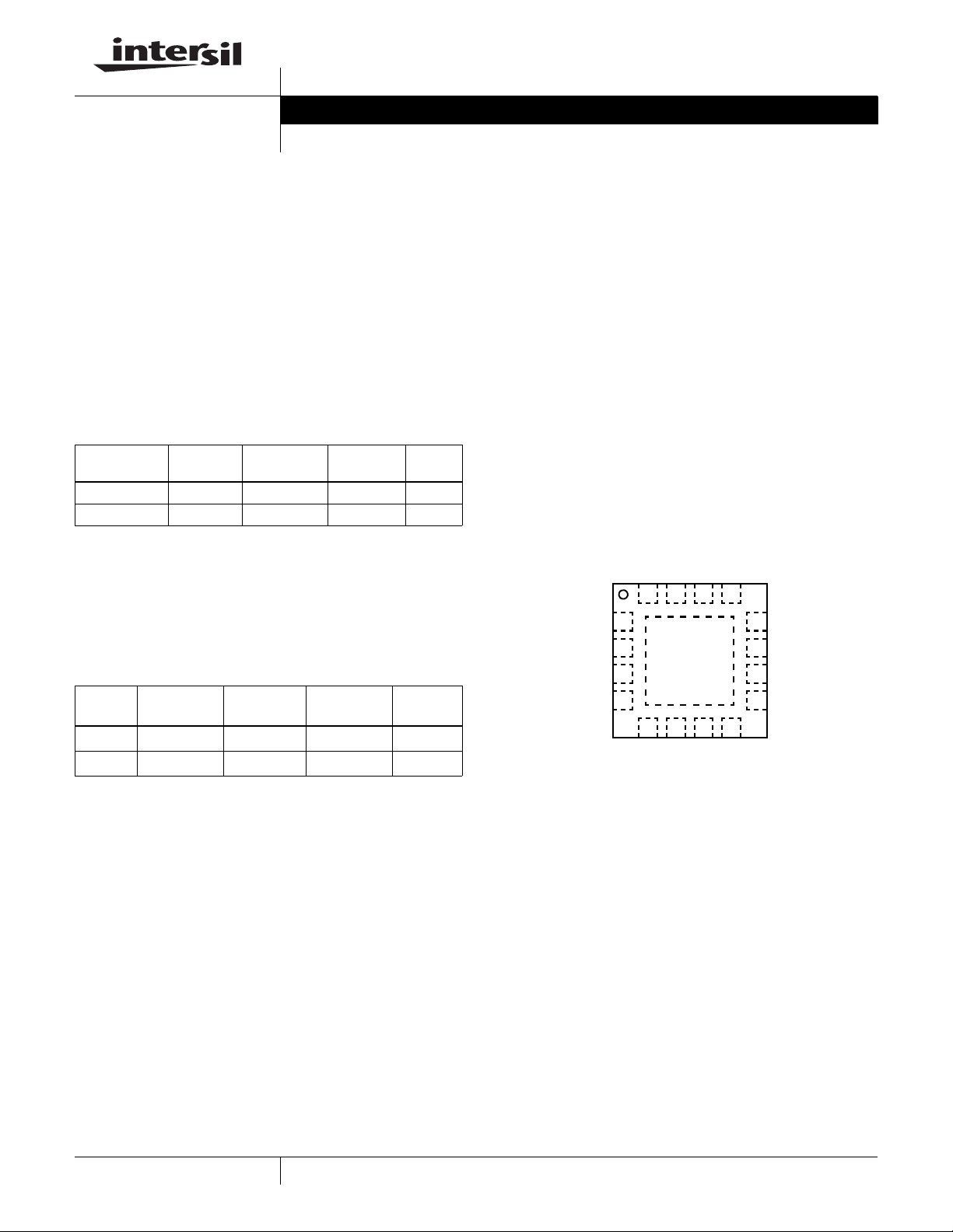
Pinout
ISL14010, ISL14017
(16 LD QFN)
TOP VIEW
VCC
NC
VCC
CLK4
15
16 14 13
VCC
X1
X2
GND
1
2
3
4
6578
NC
GND
GND
CLK1
12
NC
CLK3
11
10
CLK2
NC
9
1
CAUTION: These devices are sensitive to electrostatic discharge; follow proper IC Handling Procedures.
1-888-INTERSIL or 1-888-468-3774
| Intersil (and design) is a registered trademark of Intersil Americas Inc.
Copyright Intersil Americas Inc. 2006, 2007. All Rights Reserved
All other trademarks mentioned are the property of their respective owners.
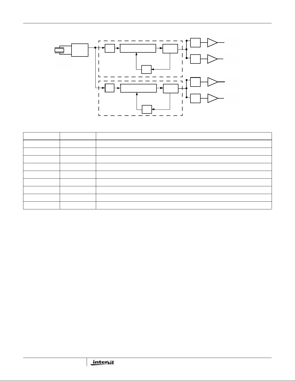
ISL14010, ISL14017
Functional Block Diagram
30MHz
CRYSTAL
OSC.
M2
PHASE FREQ DET. M1
N1
PHASE FREQ DET.
N2
VCO1
VCO2
Pin Description
16 LD QFN SYMBOLS PIN DESCRIPTION
1,14,16 VCC Supply Voltage
2 X1 The X1 pin is the terminal 1 of an external 30MHz crystal. This pin is grounded for external CK input.
3 X2 The X2 pin is the terminal 2 of external 30MHz crystal, or external clock input.
4, 5, 7 GND Ground
8 CLK1 CLK1 Output: 25MHz
10 CLK2 CLK2 Output: 30MHz
11 CLK3 CLK3 Output: 48MHz (40MHz for ISL14017)
13 CLK4 CLK4 Output: 54MHz (50MHz for ISL14017)
6, 9, 12, 15 NC No Connect
CLK1
CLK2
CLK3
CLK4
2
FN6407.1
April 16, 2007

ISL14010, ISL14017
Absolute Maximum Ratings Thermal Information
Voltage on VCC, CLK pins (respect to Gnd) . . . . . . . . -0.3V to 4.0V
Voltage on X1, X2 pins (respect to Gnd) . . . . . . . . . . . -0.3V to 2.5V
ESD Rating
MIL STD-883, Method 3014. . . . . . . . . . . . . . . . . . . . . . . . .>±5kV
Machine Model. . . . . . . . . . . . . . . . . . . . . . . . . . . . . . . . . . .>500V
CAUTION: Stresses above those listed in “Absolute Maximum Ratings” may cause permanent damage to the device. This is a stress only rating and operation of the
device at these or any other conditions above those indicated in the operational sections of this specification is not implied.
NOTE:
is measured in free air with the component mounted on a high effective thermal conductivity test board with “direct attach” features. See
1. θ
JA
Tech Brief TB379.
Thermal Resistance (Typical, Note 1) θ
(°C/W) θJC (°C/W)
JA
16 Ld QFN Package. . . . . . . . . . . . . . . 58 11
Storage Temperature. . . . . . . . . . . . . . . . . . . . . . . .-65ºC to +150ºC
Pb-free reflow profile . . . . . . . . . . . . . . . . . . . . . . . . . .see link below
http://www.intersil.com/pbfree/Pb-FreeReflow.asp
DC Electrical Specifications V
= 3.3V ±10%, TA = -40ºC to +85ºC, Typical values are at TA = +25ºC and VCC = 3.3V,
CC
Unless otherwise noted
SYMBOL SYMBOL CONDITIONS MIN TYP MAX UNIT
Supply Voltage V
Supply Current I
CC
Supply Voltage 3.0 3.3 3.6 V
CC
Supply Current CL = 5pF on all outputs 11 15 mA
CLOCK INPUT X2 (X1 GROUNDED) FOR EXTERNAL CLOCK MODE
Input High Level V
Input Level Low V
IH
IL
Input Current IIL, IIH V
to Ground 0.5 mA
X2
1.5 2.4 V
0.5 V
CLOCK OUTPUTS (CLK)
Output High Level V
Output Low Level V
OH IOH
OL
Output Short Circuit Current IOSC CLK = V
AC Electrical Specifications C
= 5pF on all outputs
L
= -100µA VCC-0.2 V
I
= -4mA 2.4 V
OH
I
= -6mA 2.1 V
OH
I
= 100µA 0.2 V
OL
I
= 4mA 0.4 V
OL
I
= 6mA 0.75 V
OL
or Gnd 6 13 30 mA
CC
SYMBOL SYMBOL CONDITIONS MIN TYP MAX UNIT
Crystal Frequency f
IN
30 MHz
CLOCK OUTPUTS
Rise Time t
Fall Time t
R
F
20% to 80% V
80% to 20% V
CC
CC
1.8 ns
1.8 ns
Duty Cycle 40 60 %
Period Jitter J
Power Up Time t
PO
RMS 50 ps
P
VCC >2.7V 2 ms
3
FN6407.1
April 16, 2007

ISL14010, ISL14017
Typical Performance Curves (Period Jitter)
70
V
= 3.3V
SUPPLY
65
TEMPERATURE +23ºC
60
55
50
45
40
35
30
PERIOD JITTER SIGMA (ps)
25
20
26
048101214
LOAD CAPACITANCE (pF)
FIGURE 1. STANDARD DEVIATION vs LOAD CAPACITANCE
CK1
CK2
CK4
CK3
All Intersil U.S. products are manufactured, assembled and tested utilizing ISO9000 quality systems.
Intersil Corporation’s quality certifications can be viewed at www.intersil.com/design/quality
Intersil products are sold by description only. Intersil Corporation reserves the right to make changes in circuit design, software and/or specifications at any time without
notice. Accordingly, the reader is cautioned to verify that data sheets are current before placing orders. Information furnished by Intersil is believed to be accurate and
reliable. However, no responsibility is assumed by Intersil or its subsidiaries for its use; nor for any infringements of patents or other rights of third parties which may result
from its use. No license is granted by implicat ion or oth erwise u nde r any p a tent or p at ent r ights of Intersil or its subsidiari es.
For information regarding Intersil Corporation and its products, see www.intersil.com
4
FN6407.1
April 16, 2007

Package Outline Drawing
L16.3x3
16 LEAD QUAD FLAT NO-LEAD PLASTIC PACKAGE
Rev 2, 4/07
3.00
6
PIN 1
INDEX AREA
ISL14010, ISL14017
A
B
4X
1.5
0.50
12X
13
12
16
6
PIN #1 INDEX AREA
1
(4X)
( 2. 80 TYP )
( 1. 50 )
0.15
TOP VIEW
3.00
( 12X 0 . 5 )
( 16X 0 . 23 )
( 16X 0 . 60)
0 . 90 ± 0.1
1 .50 ± 0 . 15
9
8
16X 0.40 ± 0.10
BOTTOM VIEW
BOTTOM VIEW
5
4
0.10
4
16X 0.23
SEE DETAIL "X"
BASE PLANE
BCMA
+ 0.07
- 0.05
C
0.10
SEATING PLANE
C
0.08
C
SIDE VIEW
0 . 00 MIN.
0 . 05 MAX.
5
0 . 2 REF
C
TYPICAL RECOMMENDED LAND PATTERN
5
DETAIL "X"
NOTES:
Dimensions are in millimeters.1.
Dimensions in ( ) for Reference Only.
2.
Dimensioning and tolerancing conform to AMSE Y14.5m-1994.
3.
Unless otherwise specified, tolerance : Decimal ± 0.05
4.
Dimension b applies to the metallized terminal and is measured
between 0.15mm and 0.30mm from the terminal tip.
Tiebar shown (if present) is a non-functional feature.
5.
The configuration of the pin #1 identifier is optional, but must be
6.
located within the zone indicated. The pin #1 indentifier may be
either a mold or mark feature.
FN6407.1
April 16, 2007
 Loading...