

Page 1

®
ISL1219
Real Time Clock/Calendar with Event Detection
Data Sheet August 14, 2006
Low Power RTC with Battery Backed
SRAM and Event Detection
The ISL1219 device is a low power real time clock with
Event Detect and Time Stamp function, timing and crystal
compensation, clock/calendar, power fail indicator, periodic
or polled alarm, intelligent battery backup switching and 2
Bytes of battery-backed user SRAM.
The oscillator uses an external, low-cost 32.768kHz crystal.
The real time clock tracks time with separate registers for
hours, minutes, and seconds. The device has calendar
registers for date, month, year and day of the week. The
calendar is accurate through 2099, with automatic leap year
correction.
Ordering Information
PART
NUMBER
(See Note)
ISL1219IUZ 1219Z 2.7V to 5.5V -40 to +85 10 Ld MSOP
ISL1219IUZ-T 1219Z 2.7V to 5.5V -40 to +85 10 Ld MSOP
NOTE: Intersil Pb-free products employ special Pb-free material sets;
molding compounds/die attach materials and 100% matte tin plate
termination finish, which are RoHS compliant and compatible with both
SnPb and Pb-free soldering operations. Intersil Pb-free products are
MSL classified at Pb-free peak reflow temperatures that meet or
exceed the Pb-free requirements of IPC/JEDEC J STD-020.
PART
MARKING
V
DD
RANGE
TEMP
RANGE
(°C)
PACKAGE
(Pb-Free)
Tape and Reel
Pinout
ISL1219
(10 LD MSOP)
TOP VIEW
X1
1
X2
2
V
BAT
3
GND
4
EVIN
5 6
10
9
8
7
V
DD
IRQ/F
SCL
SDA
EVDET
OUT
FN6314.1
Features
• Real Time Clock/Calendar
- Tracks Time in Hours, Minutes, and Seconds
- Day of the Week, Day, Month, and Year
• Security and Event Functions
- Tamper detection with Time Stamp in Normal and
Battery Backed modes
- Event Detection During Battery Backed or Normal
Modes
- Selectable Event Input Sampling Rates Allows Low
Power Operation
- Selectable Glitch Filter on Event Input Monitor
• 15 Selectable Frequency Outputs
• Single Alarm
- Settable to the Second, Minute, Hour, Day of the Week,
Day, or Month
- Single Event or Pulse Interrupt Mode
• Automatic Backup to Battery or Super Cap
• Power Failure Detection
• On-Chip Oscillator Compensation
• 2 Bytes Battery-Backed User SRAM
2
C Interface
•I
- 400kHz Data Transfer Rate
• 400nA Battery Supply Current
• Small Package
-10 Ld MSOP
• Pb-Free Plus Anneal Available (RoHS Compliant)
Applications
• Utility Meters
• Set Top Box/Modem
• POS Equipment
• Network Routers, Hubs, Switches, Bridges
• Cellular Infrastructure Equipment
• Fixed Broadband Wireless Equipment
• Test Meters/Fixtures
• Vending Machine Management
• Security and Anti Tampering Applications
- Panel/Enclosure Status
- Warranty Reporting
- Time Stamping Applications
- Patrol/Security Check (Fire or Light Equipment)
- Automotive Applications
1
CAUTION: These devices are sensitive to electrostatic discharge; follow proper IC Handling Procedures.
1-888-INTERSIL or 1-888-468-3774
| Intersil (and design) is a registered trademark of Intersil Americas Inc.
All other trademarks mentioned are the property of their respective owners.
Copyright Intersil Americas Inc. 2006. All Rights Reserved
Page 2
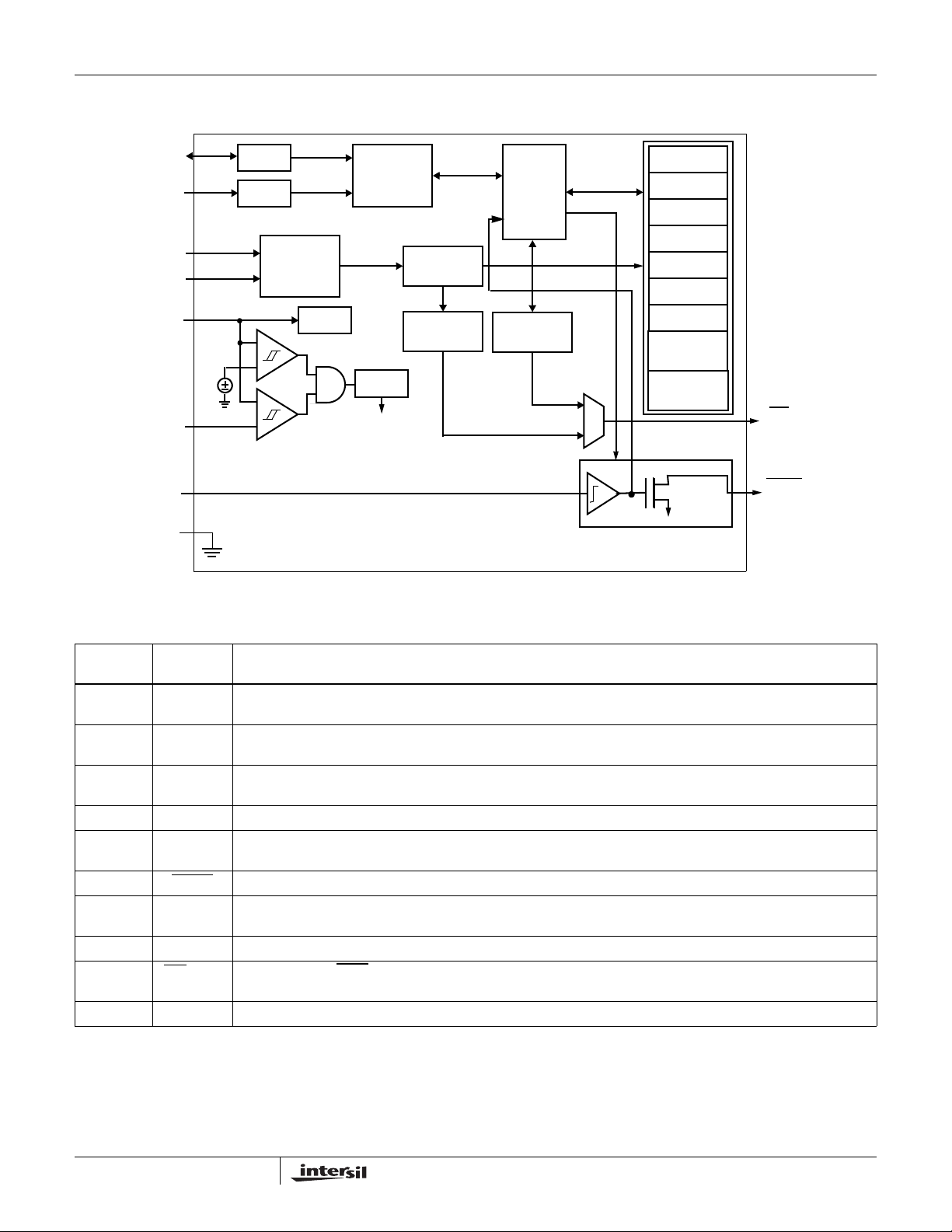
Block Diagram
ISL1219
SDA
SCL
V
DD
V
BAT
EVIN
GND
X1
X2
V
TRIP
SDA
BUFFER
SCL
BUFFER
CRYSTAL
OSCILLATOR
POR
I2C
INTERFACE
SWITCH
INTERNAL
SUPPLY
RTC
DIVIDER
FREQUENCY
OUT
CONTROL
LOGIC
ALARM
SECONDS
MINUTES
HOURS
DA Y OF WEEK
DATE
MONTH
YEAR
CONTROL
REGISTERS
USER
SRAM
IRQ/
F
OUT
EVDET
Pin Descriptions
PIN
NUMBER SYMBOL DESCRIPTION
1X1X1. The X1 pin is the input of an inverting amplifier and is intended to be connected to one pin of an external
32.768kHz quartz crystal. X1 can a l s o be d r i v e n di r e c t l y from a 32 . 7 6 8 k H z so u r c e .
2X2X2. The X2 pin is the output of an inverting amplifier and is intended to be connected to one pin of an external
32.768kHz quartz crystal. X2 should be left open when X1 is driven from external source.
3V
BAT
4GNDGround.
5EVINEvent Input (EVIN). The EVIN is an input pin that is used to detect an externally monitored event. When a high signal
6 EVDET
7SDASerial Data (SDA). SDA is a bidirectional pin used to transfer serial data into and out of the device. It has an open
8SCLSerial Clock (SCL). The SCL input is used to clock all serial data into and out of the device.
9IRQ
10 V
/F
DD
V
This input provides a backup supply voltage to the device. V
BAT.
the V
supply fails. This pin should be tied to ground if not used.
DD
BAT
is present at the EVIN pin an “event” is detected.
Event Detect Output, active when EVIN is triggered. Open drain output.
drain output and may be wire OR’ed with other open drain or open collector outputs.
Interrupt Output IRQ, /Frequency Output F
OUT
output pin. The function is set via the configuration register.
V
Power supply.
DD.
Multi-functional pin that can be used as interrupt or frequency
OUT.
supplies power to the device in the event that
2
FN6314.1
August 14, 2006
Page 3

ISL1219
Absolute Maximum Ratings Thermal Information
Voltage on VDD, V
(respect to ground). . . . . . . . . . . . . . . . . . . . . . . . . . -0.5V to 7.0V
, SCL, SDA, and IRQ/F
BAT
OUT
Pins
Voltage on X1 and X2 Pins
(respect to ground). . . . . . . . . . . .-0.5V to V
-0.5V to V
Storage Temperature. . . . . . . . . . . . . . . . . . . . . . . .-65°C to +150°C
+ 0.5 (VDD Mode)
DD
+ 0.5 (V
BAT
BAT
Mode)
Lead Temperature (Soldering, 10s) . . . . . . . . . . . . . . . . . . . . .300°C
ESD Rating (Human Body Model). . . . . . . . . . . . . . . . . . . . . . .>2kV
ESD Rating (Machine Model . . . . . . . . . . . . . . . . . . . . . . . . . .>175V
CAUTION: Stresses above those listed in “Absolute Maximum Ratings” may cause permanent damage to the device. This is a stress only rating and operation of the
device at these or any other conditions above those indicated in the operational sections of this specification is not implied.
NOTE:
is measured with the component mounted on a high effective thermal conductivity test board in free air. See Tech Brief TB379 for details.
1. θ
JA
Thermal Resistance (Typical, Note 1)
θ
(°C/W)
JA
10 Ld MSOP Package . . . . . . . . . . . . . . . . . . . . . . . 120
Moisture Sensitivity (see Technical Brief TB363). . . . . . . . . . Level 2
DC Operating Characteristics – RTC Test Conditions: V
= +2.7 to +5.5V, Temperature = -40°C to +85°C, unless otherwise stated.
DD
SYMBOL PARAMETER CONDITIONS MIN
V
DD
V
BAT
I
DD1
I
DD2
I
DD3
I
BAT
I
BATLKG
I
LI
I
LO
V
TRIP
V
TRIPHYS
V
BATHYS
Main Power Supply 2.7 5.5 V
Battery Supply Voltage 1.8 5.5 V
Supply Current VDD = 5V 2 6 µA 2, 3
V
= 3V 1.2 4 µA
DD
Supply Current With I2C Active VDD = 5V 40 120 µA 2, 3
Supply Current (Low Power Mode) VDD = 5V, LPMODE = 1 1.4 5 µA 2, 8
Battery Supply Current V
Battery Input Leakage VDD = 5.5V, V
= 3V 400 950 nA 2
BAT
= 1.8V 100 nA
BAT
Input Leakage Current on SCL 100 nA
I/O Leakage Current on SDA 100 nA
V
Mode Threshold 1.6 2.2 2.64 V
BAT
V
Hysteresis 10 35 60 mV
TRIP
V
Hysteresis 10 50 100 mV
BAT
EVIN
V
IL
V
IH
-0.3 0.3 x
0.7 x
V
DD
Hysteresis 0.05 x
V
DD
I
EVPU
IRQ
V
OL
I
LO
/F
OUT
EVIN Pull-up Current V
= 3V 1.5 µA 6
SUP
and EVDET
Output Low Voltage VDD = 5V, IOL = 3mA 0.4 V
V
= 2.7V, IOL = 1mA 0.4 V
DD
Output Leakage Current VDD = 5.5V
V
= 5.5V
OUT
TYP
(Note 5) MAX UNITS NOTES
V
V
DD
VDD +
V
0.3
V
100 400 nA
3
FN6314.1
August 14, 2006
Page 4

ISL1219
Power-Down Timing Test Conditions: V
= +2.7 to +5.5V, Temperature = -40°C to +85°C, unless otherwise stated.
DD
SYMBOL PARAMETER CONDITIONS MIN
V
DD SR-
I2C Interface Specifications Test Conditions: V
VDD Negative Slew Rate 10 V/ms 4
= +2.7 to +5.5V, Temperature = -40°C to +85°C, unless otherwise specified.
DD
SYMBOL PARAMETER TEST CONDITIONS MIN
V
IL
V
IH
SDA and SCL Input Buffer LOW
Voltage
SDA and SCL Input Buffer HIGH
Voltage
-0.3 0.3 x
0.7 x
V
DD
Hysteresis SDA and SCL Input Buffer Hysteresis 0.05 x
V
DD
V
OL
Cpin SDA and SCL Pin Capacitance T
f
SCL
t
IN
t
AA
SDA Output Buffer LOW Voltage,
VDD = 5V, IOL = 3mA 0.4 V
Sinking 3mA
= 25°C, f = 1MHz, VDD=5V,
A
V
=0V, V
IN
OUT
=0V
SCL Frequency 400 kHz
Pulse Width Suppression Time at
SDA and SCL Inputs
SCL Falling Edge to SDA Output Data
Valid
Any pulse narrower than the max spec
is suppressed.
SCL falling edge crossing 30% of VDD,
until SDA exits the 30% to 70% of V
DD
window.
t
BUF
t
LOW
t
HIGH
t
SU:STA
t
HD:STA
t
SU:DAT
t
HD:DAT
t
SU:STO
t
HD:STO
t
DH
t
R
Time the Bus Must be Free before the
Start of a New Transmission
SDA crossing 70% of VDD during a
STOP condition, to SDA crossing 70%
of V
during the following START
DD
condition.
Clock LOW Time Measured at the 30% of VDD crossing. 1300 ns
Clock HIGH Time Measured at the 70% of VDD crossing. 600 ns
START Condition Setup Time SCL rising edge to SDA falling edge.
Both crossing 70% of V
DD
.
START Condition Hold Time From SDA falling edge crossing 30%
of V
to SCL falling edge crossing
DD
70% of V
DD
.
Input Data Setup Time From SDA exiting the 30% to 70% of
V
window, to SCL rising edge
DD
crossing 30% of V
DD.
Input Data Hold Time From SCL falling edge crossing 30%
of V
to SDA entering the 30% to
DD
70% of V
window.
DD
STOP Condition Setup Time From SCL rising edge crossing 70% of
V
, to SDA rising edge crossing 30%
DD
of V
.
DD
STOP Condition Hold Time From SDA rising edge to SCL falling
edge. Both crossing 70% of V
DD
.
Output Data Hold Time From SCL falling edge crossing 30%
of V
, until SDA enters the 30% to
DD
70% of V
SDA and SCL Rise Time From 30% to 70% of V
window.
DD
DD.
1300 ns
600 ns
600 ns
100 ns
0 900 ns
600 ns
600 ns
0ns
20 +
0.1 x Cb
TYP
(Note 5) MAX UNITS NOTES
TYP
(Note 4) MAX UNITS NOTES
V
V
DD
VDD +
V
0.3
V
10 pF
50 ns
900 ns
300 ns 7
4
FN6314.1
August 14, 2006
Page 5
ISL1219
I2C Interface Specifications Test Conditions: V
= +2.7 to +5.5V, Temperature = -40°C to +85°C, unless otherwise specified.
DD
TYP
SYMBOL PARAMETER TEST CONDITIONS MIN
t
F
SDA and SCL Fall Time From 70% to 30% of V
DD.
20 +
(Note 4) MAX UNITS NOTES
300 ns 7
0.1 x Cb
Cb Capacitive Loading of SDA or SCL Total on-chip and off-chip 10 400 pF 7
Rpu SDA and SCL Bus Pull-up Resistor
Off-chip
Maximum is determined by t
For Cb = 400pF, max is about
and tF.
R
1kΩ 7
2~2.5kΩ. For Cb = 40pF, max is about
15~20kΩ
NOTES:
2. IRQ
and F
and EVDET Inactive.
OUT
3. LPMODE = 0 (default).
4. In order to ensure proper timekeeping, the V
specification must be followed.
DD SR-
5. Typical values are for T = 25°C and 3.3V supply voltage.
6. V
7. These are I
= VDD if in V
SUP
2
C specific parameters and are not directly tested, however they are used during device testing to validate device specification.
8. A write to register 08h should only be done if V
DD
Mode, V
SUP
= V
BAT
if in V
DD
Mode.
BAT
> V
, otherwise the device will be unable to communicate using I2C.
BAT
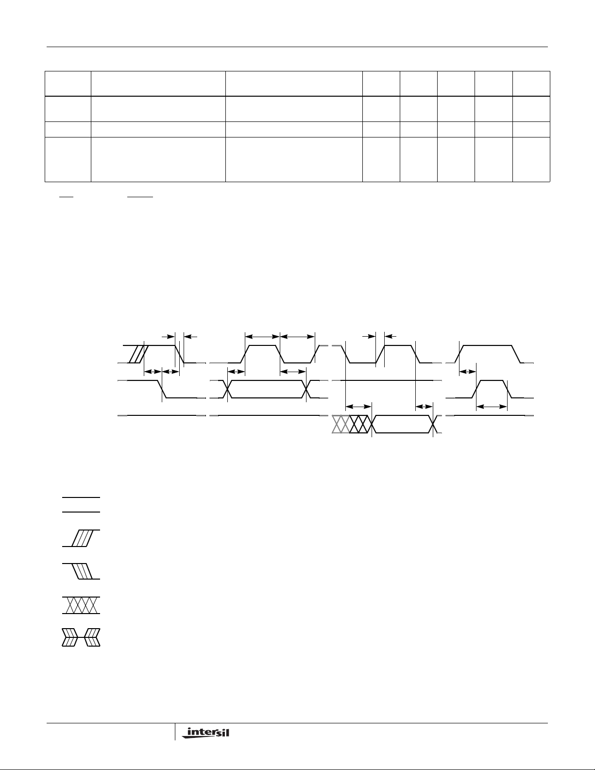
SDA vs. SCL Timing
t
F
t
HIGH
t
LOW
t
R
SCL
t
(INPUT TIMING)
(OUTPUT TIMING)
SDA
SDA
SU:STA
t
HD:STA
Symbol Table
WAVEFORM INPUTS OUTPUTS
Must be steady Will be steady
May change
from LOW
to HIGH
May change
from HIGH
to LOW
Don’t Care:
Changes Allowed
N/A Center Line is
t
SU:DAT
Will change
from LOW
to HIGH
Will change
from HIGH
to LOW
Changing:
State Not Known
High Impedance
t
HD:DAT
t
SU:STO
t
DH
t
AA
t
BUF
5
FN6314.1
August 14, 2006
Page 6
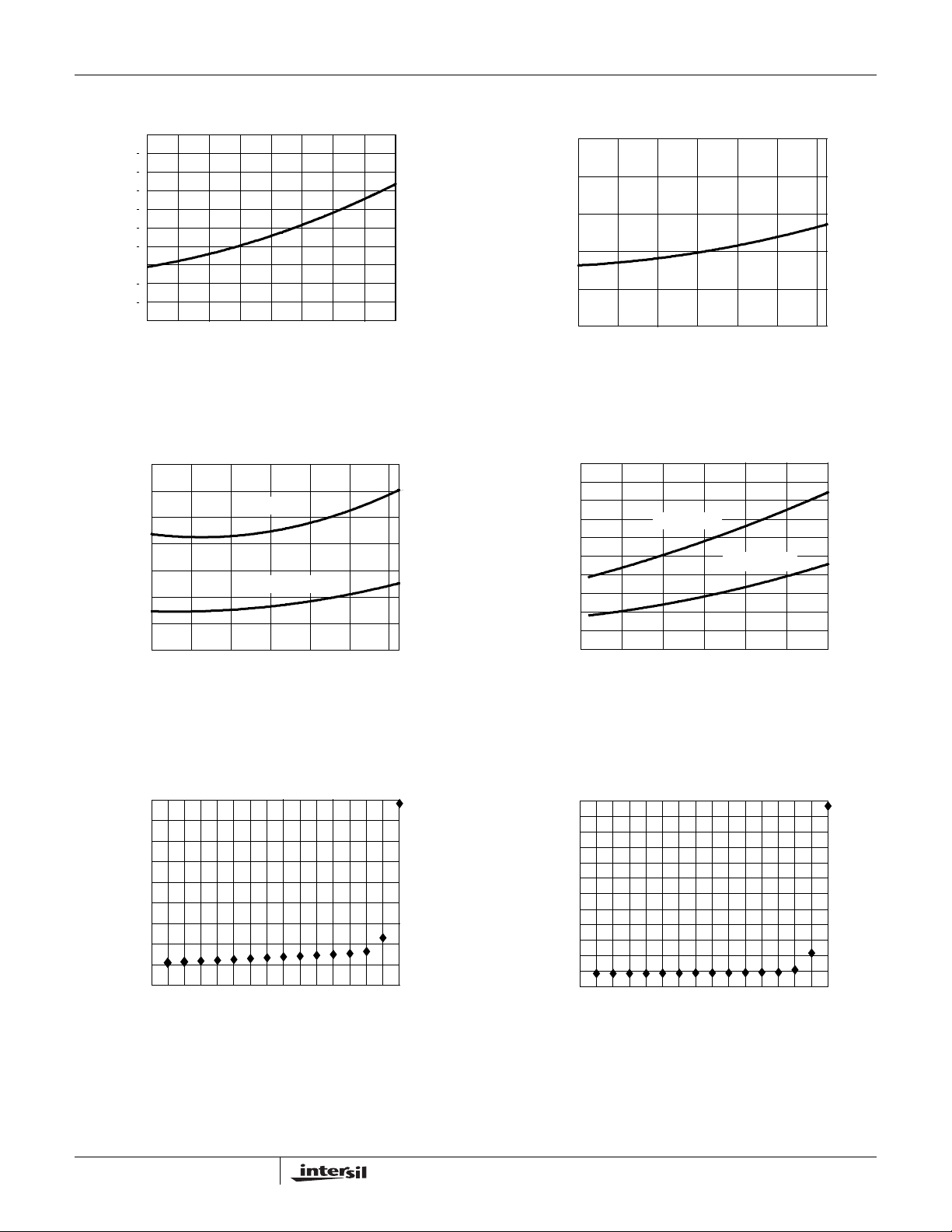
ISL1219
VDD
Typical Performance Curves Temperature is +25°C unless otherwise specified
900E-9
800E-9
700E-9
600E-9
(A)
500E-9
BAT
I
400E-9
300E-9
200E-9
100E-9
000E+0
2.4E-06
2.2E-06
2.0E-06
1.8E-06
(A)
1.6E-06
DD1
I
1.4E-06
1.2E-06
1.0E-06
1E-6
1.5 2.0 2.5 3.0 3.5 4.0 4.5 5.0 5.5
(V)
V
BAT
FIGURE 1. I
-40-200 20406080
TEMPERATURE (°C)
FIGURE 3. I
DD1
vs V
BAT
VDD= 5V
VDD= 3.3V
BAT
vs TEMPERATURE FIGURE 4. I
1E-6
800E-9
600E-9
(A)
BAT
I
400E-9
200E-9
000E+0
FIGURE 2. I
2.4E-6
2.2E-6
2.0E-6
1.8E-6
1.6E-6
(A)
1.4E-6
DD1
I
1.2E-6
1.0E-6
800.0E-9
600.0E-9
400.0E-9
-40-200 20406080
TEMPERATURE (°C)
vs TEMPERATURE AT V
BAT
LPMODE = 0
LPMODE = 1
2.53.03.54.04.55.05.5
V
(V)
DD
vs VDD WITH LPMODE ON AND OFF
DD1
BAT
= 3V
(A)
DD1
I
2.1E-6
2.0E-6
1.9E-6
1.8E-6
1.7E-6
1.6E-6
1.5E-6
1.4E-6
1.3E-6
1.2E-6
1/8
1/32
1/16
FIGURE 5. I
1/4
DD1
1
1/2
F
OUT (Hz)
vs F
6
2
OUT
4
AT V
3.0E-6
2.9E-6
2.8E-6
2.7E-6
2.6E-6
2.5E-6
(A)
2.4E-6
DD1
2.3E-6
I
2.2E-6
2.1E-6
2.0E-6
1.9E-6
8
16
64
32
DD
4096
1024
32768
= 3.3V FIGURE 6. I
1.8E-6
1
4
2
8
16
64
1/16
DD1
F
OUT (Hz)
vs F
OUT
1/2
1/4
1/8
1/32
32
AT VDD = 5V
4096
1024
32768
FN6314.1
August 14, 2006
Page 7
D
ISL1219
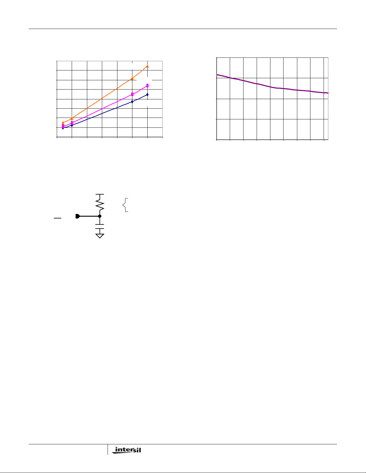
Typical Performance Curves Temperature is +25°C unless otherwise specified (Continued)
8.00E-06
7.00E-06
6.00E-06
5.00E-06
4.00E-06
PULLUP
I
3.00E-06
2.00E-06
1.00E-06
0.00E+00
2.533.544.555.56
V
D
FIGURE 7. EVIN I
EQUIVALENT AC OUTPUT LOAD CIRCUIT FOR V
SDA
AND
/FOUT
IRQ
FIGURE 9. STANDARD OUTPUT LOAD FOR TESTING THE
DEVICE WITH V
5.0V
DD
PULL-UP
1533Ω
100pF
= 5.0V
-40°C
vs V
DD
FOR VOL= 0.4V
AND I
+25°C
+85°C
DD
= 3mA
OL
= 5V
5.0E-07
4.0E-07
3.0E-07
PULLUP
I
2.0E-07
1.0E-07
-40 -25 -10 5 20 35 50 65 80
Temperature
FIGURE 8. I
PULL-UP
vs TEMPERATURE AT V
BAT
= 1.8V
hours, minutes, and seconds. The device has calendar
registers for date, month, year and day of the week. The
calendar is accurate through 2099, with automatic leap year
correction.
The ISL1219's alarm can be set to any clock/calendar value
for a match. For example, every minute, every Tuesday or at
5:23 AM on March 21. The alarm status is available by
checking the Status Register, or the device can be
configured to provide a hardware interrupt via the IRQ pin.
There is a repeat mode for the alarm allowing a periodic
interrupt every minute, every hour, every day, etc.
General Description
The ISL1219 device is a low power Real Time Clock with
Security and Event function, Time Stamp in both normal and
battery modes, timing and crystal compensation,
clock/calendar, power fail indicator, periodic or polled alarm,
intelligent battery backup switching, and battery-backed user
SRAM.
The Event Detection function can be used for tamper
detection, security or other chassis or generic system
monitoring. Upon a valid event detection, the ISL1219 sets
the Event Detection bit (EVT bit) in the status register, stores
time stamp information on on board memory, and, can
optionally: 1) Issue an Event Output signal (EVDET pin), 2)
At the time the event occurred, stop the RTC registers from
advancing. The event monitor and time stamp functions in
both main V
monitor can also be configured for various input detection
rates to optimize power consumption for the application. In
addition, the Event Monitor pin (EVIN) has a selectable glitch
filter to avoid switch de-bouncing.
The oscillator uses an external, low-cost 32.768kHz crystal.
The real time clock tracks time with separate registers for
and battery back up modes. The event
DD
The device also offers a backup power input pin. This V
BAT
pin allows the device to be backed up by battery or
SuperCap with automatic switchover from V
entire ISL1219 device is fully operational from V
DD
to V
DD
. The
BAT
=2.7V to
5.5V and the clock/calendar portion of the device remains
fully operational in battery backup mode down to 1.8V
(Standby Mode).
Pin Description
X1, X2
The X1 and X2 pins are the input and output, respectively, of
an inverting amplifier. An external 32.768kHz quartz crystal
is used with the ISL1219 to supply a timebase for the real
time clock. Internal compensation circuitry provides high
accuracy over the operating temperature range from
-40°C to +85°C. This oscillator compensation network can
be used to calibrate the crystal timing accuracy over
temperature either during manufacturing or with an external
temperature sensor and microcontroller for active
compensation. The device can also be driven directly from a
32.768kHz source at pin X1.
7
FN6314.1
August 14, 2006
Page 8

X1
X2
FIGURE 10. RECOMMENDED CRYSTAL CONNECTION
V
BAT
This input provides a backup supply voltage to the device.
V
supplies power to the device in the event that the VDD
BAT
supply fails. This pin can be connected to a battery, a Super
Cap or tied to ground if not used.
EVIN (Event Input)
The EVIN pin is an input that is used to detect an externally
monitored event. When a high signal is present at the EVIN
pin, an “event” is detected. This input may be used for
various monitoring functions, such as the opening of a
detection switch on a chassis or door. The event detection
circuit can be user enabled or disabled (see EVEN bit) and
provides the option to be operational in battery backup
modes (see EVBATB bit). When the event detection is
disabled the EVIN pin is gated OFF. See functional
Description for more details.
EVDET (Event Detect Output)
The EVDET is an open drain output which will go low when
an event is detected at the EVIN pin. If the event detection
function is enabled, the EVDET
output will go low and stay
low until the EVT bit is cleared (see EVIN pin description).
IRQ/F
(Interrupt Output/Frequency Output)
OUT
This dual function pin can be used as an interrupt or
frequency output pin. The IRQ
/F
mode is selected via
OUT
the frequency out control bits of the control/status register.
• Interrupt Mode. The pin provides an interrupt signal
output. This signal notifies a host processor that an alarm
has occurred and requests action. It is an open drain
active low output.
• Frequency Output Mode. The pin outputs a clock signal
which is related to the crystal frequency. The frequency
output is user selectable and enabled via the I
2
C bus. It is
an open drain active low output.
Serial Clock (SCL)
The SCL input is used to clock all serial data into and out of
the device. The input buffer on this pin is always active (not
gated). It is disabled when the backup power supply on the
V
pin is activated to minimize power consumption.
BAT
Serial Data (SDA)
SDA is a bidirectional pin used to transfer data into and out
of the device. It has an open drain output and may be ORed
with other open drain or open collector outputs. The input
buffer is always active (not gated) in normal mode.
ISL1219
An open drain output requires the use of a pull-up resistor.
The output circuitry controls the fall time of the output signal
with the use of a slope controlled pull-down. The circuit is
designed for 400kHz I
when the backup power supply on the V
2
C interface speeds. It is disabled
pin is activated.
BAT
VDD, GND
Chip power supply and ground pins. The device will operate
with a power supply from V
capacitor is recommended on the V
= 2.7V to 5.5VDC. A 0.1µF
DD
pin to ground.
DD
Functional Description
Power Control Operation
The power control circuit accepts a VDD and a V
Many types of batteries can be used with Intersil RTC
products. For example, 3.0V or 3.6V Lithium batteries are
appropriate, and battery sizes are available that can power
the ISL1219 for up to 10 years. Another option is to use a
Super Cap for applications where V
is interrupted for up
DD
to a month. See the Applications Section for more
information.
Normal Mode (VDD) to Battery Backup Mode
(V
)
BAT
To transition from the VDD to V
following conditions must be met:
Condition 1:
V
< V
DD
where V
- V
BAT
BATHYS
BATHYS
≈ 50mV
Condition 2:
VDD < V
where V
TRIP
TRIP
≈ 2.2V
Battery Backup Mode (V
(V
)
DD
The ISL1219 device will switch from the V
when one
Condition 1:
Condition 2:
of the following conditions occurs:
V
> V
DD
where V
VDD > V
where V
+ V
BAT
BATHYS
+ V
TRIP
TRIPHYS
BATHYS
≈ 50mV
TRIPHYS
≈ 30mV
mode, both of the
BAT
) to Normal Mode
BAT
BAT
input.
BAT
to VDD mode
8
FN6314.1
August 14, 2006
Page 9

ISL1219
These power control situations are illustrated in Figures 11
and 12.
BATTERY BACKUP
V
DD
V
TRIP
V
BAT
V
- V
BAT
BATHYS
FIGURE 11. BATTERY SWITCHOVER WHEN V
V
DD
V
BAT
V
TRIP
V
TRIP
MODE
BATTERY BACKUP
MODE
V
V
BAT
TRIP
+ V
BAT
+ V
2.2V
1.8V
BATHYS
< V
3.0V
2.2V
TRIPHYS
TRIP
Low Power Mode is useful in systems where V
higher than V
V
to V
DD
BAT
at all times. The device will switch from
BAT
when VDD drops below V
BAT
of hysteresis to prevent any switchback of V
switchover. In a system with a V
battery of V
= 3V, Low Power Mode can be used.
BAT
= 5V and backup lithium
DD
is normally
DD
, with about 50mV
after
DD
However, it is not recommended to use Low Power Mode in
a system with V
there is a finite I-R voltage drop in the V
= 3.3V ±10%, V
DD
≥ 3.0V, and when
BAT
line.
DD
InterSeal™ Battery Saver
The ISL1219 has the InterSeal™ Battery Saver which
prevents initial battery current drain before it is first used. For
example, battery-backed RTCs are commonly packaged on
a board with a battery connected. In order to preserve
battery life, the ISL1219 will not draw any power from the
battery source until after the device is first powered up from
the V
battery backup mode whenever V
source. Thereafter, the device will switchover to
DD
power is lost.
DD
Event/Tamper Monitor and Detection
The ISL1219 provides an event detection, time stamp and
alarm function to be used in a wide variety of applications
ranging from security, warranty monitoring, data collection
and recording.
FIGURE 12. BATTERY SWITCHOVER WHEN V
BAT
> V
TRIP
The I2C bus is deactivated in battery backup mode to provide
lower power. Asi de fro m this, all R T C fu nctions are
operational during battery backup mode. Except for SCL and
SDA, all the inputs and outputs of the ISL1219 are active
during battery backup mode unless disabled via the control
register. The User SRAM is operationa l in battery backup
mode down to 1.8V.
Power Failure Detection
The ISL1219 provides a Real Time Clock Failure Bit (RTCF)
to detect total power failure. It allows users to determine if
the device has powered up after having lost all power to the
device (both V
DD
and V
BAT
).
Low Power Mode
The normal power switching of the ISL1219 is designed to
switch into battery backup mode only if the V
lost. This will ensure that the device can accept a wide range
of backup voltages from many types of sources while reliably
switching into backup mode. Another mode, called Low
Power Mode, is available to allow direct switching from V
to V
the additional monitoring of V
without requiring VDD to drop below V
BAT
DD
vs. V
TRIP
needed, that circuitry is shut down and less power is used
while operating from V
600nA at V
= 5V. Low Power Mode is activated via the
DD
. Power savings are typically
DD
LPMODE bit in the control and status registers.
power is
DD
. Since
TRIP
is no longer
DD
The tamper detect input pin, EVIN, can be used as a event
or tamper detection input of an external switch (mechanical
or electronic). When the EVIN pin is a valid HIGH, the
ISL1219 sets the EVT bit in the status register and, can
optionally: 1) Issue an Event output signal (EVDET
pin) and
store time stamp information in on board SRAM (second,
minute, hour, date, month and year), 2) At the time event
occurred, stop the RTC registers from advancing.
To allow for flexibility of external switches used at the EVIN
pin, the internal pull-up (~1µA in full on mode) can be
disabled/enabled. This will allow more flexibility depending
on the capacitive and resistive loading at the EVIN pin.
A noise filter option is also provided for the event monitor
circuit. The EVIN pin has a time based filter where the EVIN
signal must be stable for a period of time to trigger a valid
detection. The time hysteresis filter can vary from 0, 3.9ms,
15.2ms or 31.25ms.
For low power applications the event monitor can be
sampled at a user selectable rate. The EVIN pin can be
always ON or periodically sampled with a frequency of 1/4, 1
or 2Hz.
9
FN6314.1
August 14, 2006
Page 10

ISL1219
Event Detect Timing Diagram With
Sampling Mode Enabled
Case 1, Switched Opened Before I
15 CLKS (8x)
pu
IN
ON
OFF
OPEN
CLOSED
HIGH
LOW
HIGH
LOW
8 CLKS (8x)
I
EXT.
SWITCH
EV
EVDET
Case 2, Switched Opened After I
15 CLKS (8x)
pu
IN
ON
OFF
OPEN
CLOSED
HIGH
LOW
I
EXT.
SWITCH
EV
pu
pu
Users have the option to connect EVIN (see EVINEB bit) to
an internal pull-up current source that operates at 1
µA
(always on mode), which can drop to 400nA in battery
backup mode. User selectabl e event sampling modes are
also available which will effectively reduce power
consumption with 1/4-Hz, 1-Hz and 2-Hz sample detection
rates. The EVIN input is pulsed ON/OFF when in sampling
mode for power savings advantages (See tables below).
The EVIN also has a user selectable time based hysteresis
filter (see EHYS bits) to implement switch de-bouncing
during an event detection. The EVIN signal must be high for
the duration of the selected time period. The time periods
available are 0 times delay (no time based hysteresis) to
3.9ms, 15.625ms or 31.25ms (see Table 1, 2, 3, and 4).
TABLE 1. ∆I
f
SMP
DD (VDD
1/4Hz 20.5nA
1Hz 82nA
2Hz 164nA
TABLE 2. ∆I
f
SMP
DD (VDD
1/4Hz 65.8nA
1Hz 263.3nA
2Hz 526.5nA
=3V, t
=5.0V, t
HYS
HYS
=3.9ms)
DELTA I
=3.9ms)
DELTA I
DD
DD
HIGH
EVDET
LOW
8 CLKS (8x)
Case 3, Switched Bounced
15 CLKS (8x)
I
EXT.
SWITCH
EV
EVDET
The ISL1219 can operate independently or in conjunction
with a microcontroller for low power operation modes or in
battery backup modes.
The event detection and time stamp circuits operate in either
main V
ON
pu
OFF
OPEN
CLOSED
HIGH
IN
LOW
HIGH
LOW
power or battery backup mode.
DD
8 CLKS (8x)
TABLE 3. ∆I
f
SMP
DD (VDD
=3.0V, t
=15.625ms)
HYS
DELTA I
DD
1/4Hz 82nA
1Hz 328nA
2Hz 656.3nA
TABLE 4. ∆I
f
SMP
DD (VDD
=5.0V, t
=15.625ms)
HYS
DELTA I
DD
1/4Hz 264nA
1Hz 1.05µA
2Hz 2.1µA
Real Time Clock Operation
The Real Time Clock (RTC) uses an external 32.768kHz
quartz crystal to maintain an accurate internal representation
of second, minute, hour, day of week, date, month, and year.
The RTC also has leap-year correction. The clock also
corrects for months having fewer than 31 days and has a bit
that controls 24 hour or AM/PM format. When the ISL1219
powers up after the loss of both V
not begin incrementing until at least one byte is written to the
clock register.
DD
and V
, the clock will
BAT
10
FN6314.1
August 14, 2006
Page 11

ISL1219
Accuracy of the Real Time Clock
The accuracy of the Real Time Clock depends on the
frequency of the quartz crystal that is used as the time base
for the RTC. Since the resonant frequency of a crystal is
temperature dependent, the RTC performance will also be
dependent upon temperature. The frequency deviation of
the crystal is a function of the turnover temperature of the
crystal from the crystal’s nominal frequency. For example, a
~20ppm frequency deviation translates into an accuracy of
~1 minute per month. These parameters are available from
the crystal manufacturer. The ISL1219 provides on-chip
crystal compensation networks to adjust load capacitance to
tune oscillator frequency from -94ppm to +140ppm. For
more detailed information see the Application Section.
Single Event and Interrupt
The alarm mode is enabled via the ALME bit. Choosing
single event or interrupt alarm mode is selected via the IM
bit. Note that when the frequency output function is enabled,
the alarm function is disabled.
The standard alarm allows for alarms of time, date, day of
the week, month, and year. When a time alarm occurs in
single event mode, an IRQ
alarm status bit (ALM) will be set to “1”.
The pulsed interrupt mode allows for repetitive or recurring
alarm functionality. Hence, once the alarm is set, the device
will continue to alarm for each occurring match of the alarm
and present time. Thus, it will alarm as often as every minute
(if only the nth second is set) or as infrequently as once a
year (if at least the nth month is set). During pulsed interrupt
mode, the IRQ
status bit (ALM) will be set to “1”.
The ALM bit can be reset by the user or cleared
automatically using the auto reset mode (see ARST bit).
The alarm function can be enabled/disabled during battery
backup mode using the FOBATB bit. For more information
on the alarm, please see the Alarm Registers Description.
pin will be pulled low for 250ms and the alarm
pin will be pulled low and the
Frequency Output Mode
The ISL1219 has the option to provide a frequency output
signal using the IRQ
is set by using the FO bits to select 15 possible output
frequency values from 0 to 32kHz. The frequency output can
be enabled/disabled during battery backup mode using the
FOBATB bit.
/F
pin. The frequency output mode
OUT
General Purpose User SRAM
The ISL1219 provides 2 bytes of user SRAM. The SRAM will
continue to operate in battery backup mode. However, it
should be noted that the I
backup mode.
2
C bus is disabled in battery
I2C Serial Interface
The ISL1219 has an I2C serial bus interface that provides
access to the control and status registers and the user
SRAM. The I
industry I
signal (SDA) and a clock signal (SCL).
2
C serial interface is compatible with other
2
C serial bus protocols using a bidirectional data
Oscillator Compensation
The ISL1219 provides the option of timing correction due to
temperature variation of the crystal oscillator for either
manufacturing calibration or active calibration. The total
possible compensation is typically -94ppm to +140ppm. Two
compensation mechanisms that are available are as follows:
1. An analog trimming (ATR) register that can be used to
adjust individual on-chip digital capacitors for oscillator
capacitance trimming. The individual digital capacitor is
selectable from a range of 9pF to 40.5pF (based upon
32.758kHz). This translates to a calculated
compensation of approximately -34ppm to +80ppm. (See
ATR description.)
2. A digital trimming register (DTR) that can be used to
adjust the timing counter by ±60ppm. (See DTR
description.)
Also provided is the ability to adjust the crystal capacitance
when the ISL1219 switches from V
mode. (See Battery Mode ATR Selection for more details.)
to battery backup
DD
Register Descriptions
The battery-backed registers are accessible following a
slave byte of “1101111x” and reads or writes to addresses
[00h:19h]. The defined addresses and default values are
described in the Table 1. Address 09h is not used. Reads or
writes to 09h will not affect operation of the device but should
be avoided.
REGISTER ACCESS
The contents of the registers can be modified by performing
a byte or a page write operation directly to any register
address.
The registers are divided into 4 sections. These are:
1. Real Time Clock (7 bytes): Address 00h to 06h.
2. Control and Status (5 bytes): Address 07h to 0Bh.
3. Alarm (6 bytes): Address 0Ch to 11h.
4. User SRAM (2 bytes): Address 12h to 13h.
5. Time Stamp (6 bytes): Address 14h to 19h
There are no addresses above 19h.
Write capability is allowable into the RTC registers (00h to
06h) only when the WRTC bit (bit 4 of address 07h) is set to
“1”. A multi-byte read or write op eratio n is limi ted to on e
section per operation. Access to another section requires a
new operation. A read or write can begin at any address
within the section.
A register can be read by performing a random read at any
address at any time. This returns the contents of that register
location. Additional registers are read by performing a
sequential read. For the RTC and Alarm registers, the read
11
FN6314.1
August 14, 2006
Page 12

ISL1219
instruction latches all clock registers into a buffer, so an
update of the clock does not change the time being read. A
sequential read will not result in the output of data from the
memory array. At the end of a read, the master supplies a
stop condition to end the operation and free the bus. After a
user can execute a current address read and continue
reading the next register.
It is not necessary to set the WRTC bit prior to writing into
the control and status, alarm, and user SRAM registers.
read, the address remains at the previous address +1 so the
TABLE 5. REGISTER MEMORY MAP
REG
ADDR. SECTION
00h
01h MN 0 MN22 MN21 MN20 MN13 MN12 MN11 MN10 0-59 00h
02h HR MIL 0 HR21 HR20 HR13 HR12 HR11 HR10 0-23 00h
03h DT 0 0 DT21 DT20 DT13 DT12 DT11 DT10 1-31 00h
04h MO 0 0 0 MO20 MO13 MO12 MO11 MO10 1-12 00h
05h YR YR23 YR22 YR21 YR20 YR13 YR12 YR11 YR10 0-99 00h
06h DW00000DW2DW1DW00-600h
07h
08h INT IM ALME LPMODE FOBATB FO3 FO2 FO1 FO0 N/A 00h
09h EV EVIENB EVBATB RTCHLT EVEN EHYS1 EHYS0 ESMP1 ESMP0 N/A 00h
0Ah ATR BMATR1 BMATR0 ATR5 ATR4 ATR3 ATR2 ATR1 ATR0 N/A 00h
0Bh DTR Reserved DTR2 DTR1 DTR0 N/A 00h
0Ch
0Dh MNA EMNA AMN22 AMN21 AMN20 AMN13 AMN12 AMN11 AMN10 00-59 00h
0Eh HRA EHRA 0 AHR21 AHR20 AHR13 AHR12 AHR11 AHR10 0-23 00h
0Fh DTA EDTA 0 ADT21 ADT20 ADT13 ADT12 ADT11 ADT10 1-31 00h
10h MOA EMOA 0 0 AMO20 AMO13 AMO12 AMO11 AMO10 1-12 00h
11h DWAEDWA0000ADW12ADW11ADW100-600h
12h
13h USR2 USR27 USR26 USR25 USR24 USR23 USR22 USR21 USR20 N/A 00h
14h
15h MNT 0 MNT22 MNT21 MNT20 MNT13 MNT12 MNT11 MNT10 00-59 00h
16h HRT MILT 0 HRT21 HRT20 HRT13 HRT12 HRT11 HRT10 0-23 00h
17h DTT 0 0 DTT21 DTT20 DTT13 DTT12 DTT11 DTT10 1-31 00h
18h MOT 0 0 0 MOT20 MOT13 MOT12 MOT11 MOT10 1-12 00h
19h YRT YRT23 YRT22 YRT21 YRT20 YRT13 YRT12 YRT11 YRT10 0-99 00h
RTC
Control
and
Status
Alarm
User
Time
Stamp
NAME
SC 0 SC22 SC21 SC20 SC13 SC12 SC11 SC10 0-59 00h
SR ARST XTOSCB Reserved WRTC EVT ALM BAT RTCF N/A 01h
SCA ESCA ASC22 ASC21 ASC20 ASC13 ASC12 ASC11 ASC10 00-59 00h
USR1 USR17 USR16 USR15 USR14 USR13 USR12 USR11 USR10 N/A 00h
SCT 0 SCT22 SCT21 SCT20 SCT13 SCT12 SCT11 SCT10 00-59 00h
BIT
RANGE DEFAULT 76543210
12
FN6314.1
August 14, 2006
Page 13

ISL1219
Real Time Clock Registers
Addresses [00h to 06h]
RTC REGISTERS (SC, MN, HR, DT, MO, YR, DW)
These registers depict BCD representations of the time. As
such, SC (Seconds) and MN (Minutes) range from 0 to 59,
HR (Hour) can either be a 12-hour or 24-hour mode, DT
(Date) is 1 to 31, MO (Month) is 1 to 12, YR (Y ear) is 0 to 99,
and DW (Day of the Week) is 0 to 6.
The DW register provides a Day of the Week status and uses
three bits DW2 to DW0 to represent the seven days of the
week. The counter advances in the cycle 0-1-2-3-4-5-6-0-12-… The assignment of a numerical value to a specific day
of the week is arbitrary and may be decided by the system
software designer. The default value is defined as “0”.
24 HOUR TIME
If the MIL bit of the HR register is “1”, the RTC uses a
24Hhour format. If the MIL bit is “0”, the RTC uses a 12-hour
format and HR21 bit functions as an AM/PM indicator with a
“1” representing PM. The clock defaults to 12-hour format
time with HR21 = “0”.
LEAP YEARS
Leap years add the day February 29 and are defined as those
years that are divisible by 4. Y ears divisible by 100 are not leap
years, unless they are also divisible by 400. This means that
the year 2000 is a leap year, the year 2100 is not. The ISL1219
does not correct for the leap year in the year 2100.
Control and Status Registers
Addresses [07h to 0Bh]
The Control and Status Registers consist of the Status
Register, Interrupt and Alarm Register , Analog T rimming and
Digital Trimming Registers.
Status Register (SR)
The Status Register is located in the memory map at
address 07h. This is a volatile register that provides either
control or status of RTC failure, battery mode, alarm trigger,
event detection, write protection of clock counter, crystal
oscillator enable and auto reset of status bits.
TABLE 6. STATUS REGISTER (SR)
ADDR 7 6 5 4 3 2 1 0
07h ARST XTOSCB reserved WRTC EVT ALM BAT RTCF
Default
00 000000
REAL TIME CLOCK FAIL BIT (RTCF)
This bit is set to a “1” after a total power failure. This is a read
only bit that is set by hardware (ISL1219 internally) when the
device powers up after having lost all power to the device.
The bit is set regardless of whether V
DD
or V
is applied
BAT
first. The loss of only one of the supplies does not set the
RTCF bit to “1”. The first valid write to the RTC section after
a complete power failure resets the RTCF bit to “0” (writing
one byte is sufficient).
BATTERY BIT (BAT)
This bit is set to a “1” when the device enters battery backup
mode. This bit can be reset either manually by the user or
automatically reset by enabling the auto-reset bit (see ARST
bit). A write to this bit in the SR can only set it to “0”, not “1”.
ALARM BIT (ALM)
These bits announce if the alarm matches the real time
clock. If there is a match, the respective bit is set to “1”. This
bit can be manually reset to “0” by the user or automatically
reset by enabling the auto-reset bit (see ARST bit). A write to
this bit in the SR can only set it to “0”, not “1”.
NOTE: An alarm bit that is set by an alarm occurring during an SR
read operation will remain set after the read operation is complete.
EVENT DETECT BIT (EVT)
The event detect bit indicates status of the event input pin
(EVIN). When the Event Detect function is enabled and the
EVIN pin is triggered, the EVT bit is set to “1” to indicate a
detection of an event, and the Time Stamp Register records
the current RTC time. A write to this bit in the SR can only
set it to “0” not “1”.
When a HIGH signal is present at the EVIN pin (or a LOW to
HIGH transition), an “event” is detected. On detection the
EVT bit is set HIGH, the open drain EVDET
pin is asserted
(pulled LOW), and the RTC time is recorded in the Time
Stamp registers. The EVT bit will be reset to LOW
• any time there is a write to the to EV Register byte
• when the EVT bit is set to 0 with a Status Register write
• when there is a read from the Status Register, with the
ARST bit set to “1” (auto-reset enabled).
If the EVT bit has not been cleared, only the initial (first
occurrence) Timestamp is retained in the Timestamp
register, subsequent triggers of the EVIN pin will not record
new timestamps. If the EVT bit is cleared to “0”, the
Timestamp register will record the time of the next event
whent the EVIN pin is triggered.
13
WRITE RTC ENABLE BIT (WRTC)
The WRTC bit enables or disables write capability into the
RTC Timing Registers. The factory default setting of this bit
is “0”. Upon initialization or power up, the WRTC must be set
to “1” to enable the RTC. Upon the completion of a valid
write (STOP), the RTC starts counting. The RTC internal
FN6314.1
August 14, 2006
Page 14

ISL1219
1Hz signal is synchronized to the STOP condition during a
valid write cycle.
CRYSTAL OSCILLATOR ENABLE BIT (XTOSCB)
This bit enables/disables the internal crystal oscillator. When
the XTOSCB is set to “1”, the oscillator is disabled, and the
X1 pin allows for an external 32kHz signal to drive the RTC.
The XTOSCB bit is set to “0” on power up.
AUTO RESET ENABLE BIT (ARST)
This bit enables/disables the automatic reset of the BAT and
ALM, EVT status bits only . When ARST bit is set to “1”, these
status bits are reset to “0” after a valid read of the Status
Register (with a valid STOP condition). When the ARST is
cleared to “0”, the user must manually reset the BAT, ALM,
and EVT bits.
INTERRUPT CONTROL REGISTER (INT)
TABLE 7. INTERRUPT CONTROL REGISTER (INT)
ADDR7 6 5 4 3210
08h IM ALME LPMODE FOBATB FO3 FO2 FO1 FO0
Default0 0 0 0 0000
The interrupt control register contains Frequency Output,
Alarm, and Battery switchover control bits.
NOTE: Writing to register 08h has restrictions. If V
byte writes to register 08h are allowed, only page writes beginning
with register 07h. If V
allowed, as well as page writes.
DD>VBAT
, then a byte write to register 08h IS
BAT>VDD
, then no
FREQUENCY OUT CONTROL BITS (FO <3:0>)
TABLE 8. FREQUENCY SELECTION OF F
FREQUENCY,
F
OUT
0 Hz0000
32768 Hz 0 0 0 1
4096 Hz 0 0 1 0
1024 Hz 0 0 1 1
64 Hz0100
32 Hz0101
16 Hz0110
8 Hz0111
4 Hz1000
2 Hz1001
1 Hz1010
1/2 Hz1011
1/4 Hz1100
1/8 Hz1101
1/16 Hz1110
1/32 Hz1111
UNITS FO3 FO2 FO1 FO0
OUT
PIN
These bits enable/disable the frequency output function and
select the output frequency at the IRQ
/F
OUT
pin. See
T able 8 for frequency selection. When the frequency mode is
enabled, it will override the alarm mode at the IRQ
/F
OUT
pin.
FREQUENCY OUTPUT AND INTERRUPT BIT (FOBATB)
This bit enables/disables the F
backup mode (i.e. V
FOBATB is set to “1” the F
power source active). When the
BAT
OUT
/IRQ pin during battery
OUT
/IRQ pin is disabled during
battery backup mode. This means that both the frequency
output and alarm output functions are disabled. When the
FOBATB is cleared to “0”, the F
/IRQ pin is enabled
OUT
during battery backup mode.
LOW POWER MODE BIT (LPMODE)
This bit enables/disables low power mode. With
LPMODE = “0”, the device will be in normal mode and the
V
supply will be used when VDD < V
BAT
V
< V
DD
power mode and the V
V
< V
DD
. With LPMODE = “1”, the device will be in low
TRIP
BAT-VBATHYS
supply will be used when
BAT
. There is a supply current saving of
about 600nA when using LPMODE = “1” with V
(See Typical Performance Curves: I
DD
- V
BAT
BATHYS
DD
vs VDD with
and
= 5V.
LPMODE ON & OFF.)
It should be noted that any writes to the LPMODE bit that
may put the device into Low Power Mode should be avoided
if V
DD<VBAT
the I2C interface (until V
, as the device will no longer communicate over
rises above V
DD
BAT
).
ALARM ENABLE BIT (ALME)
This bit enables/disables the alarm function. When the ALME
bit is set to “1”, the alarm function is enabled. When the ALME
is cleared to “0”, the alarm function is disabled. The alarm
function can operate in either a single event alarm or a periodic
interrupt alarm (see IM bit).
NOTE: When the frequency output mode is enabled, the alarm function
is disabled.
INTERRUPT/ALARM MODE BIT (IM)
This bit enables/disables the interrupt mode of the alarm
function. When the IM bit is set to “1”, the alarm will operate
in the interrupt mode, where an active low pulse width of
250ms will appear at the IRQ
/F
pin when the RTC is
OUT
triggered by the alarm as defined by the alarm registers (0Ch
to 11h). When the IM bit is cleared to “0”, the alarm will
operate in standard mode, where the IRQ
/F
OUT
pin will be
tied low until the ALM status bit is cleared to “0”.
TABLE 9.
IM BIT INTERRUPT/ALARM FREQUENCY
0 Single Time Event Set By Alarm
1 Repetitive/Recurring Time Event Set By Alarm
14
FN6314.1
August 14, 2006
Page 15

ISL1219
EVENT DETECTION REGISTER (EV)
The ISL1219 provides an easy to use event and tamper
detection circuit. The Event Detection Register configures
the functionality of the event detection circuits.
EVENT INPUT SAMPLING SELECTION BITS
(ESMP<1:0>)
These two bits select the rate of sampling of the EVIN pin to
trigger an event detection. For example, a 2Hz sampling rate
would configure the ISL1219 to check the status of the EV
pin twice a second. Slower sampling significantly reduces
the supply current drain.
TABLE 10.
ESMP1 ESMP0 EVENT SAMPLING RATE
0 0 Always ON
01 2Hz
10 1Hz
1
11
/4Hz
EVENT INPUT TIME BASE HYSTERESIS SELECTION
BITS (EHYS<1:0>)
These two bits select the time base hysteresis of the EVIN
pin to filter bouncing or noise of external event detection
circuits. The time filter can be set between 0 to 31.25 ms.
TABLE 11.
EHYS1 EHYS0 TIME BASE HYSTERESIS
0 0 0 (pull-up always on)
0 1 3.9ms
1 0 15.625ms
1 1 31.25ms
EVENT DETECT ENABLE BIT (EVEN)
This bit enables/disables the Event Detect functi on of the
ISL1219. When this bit is set to “1”, the Event Detect and
Time Stamp are active. When thi s bit is clea red to “0”, the
Event Detect and Time Stamp are disabled. Only the first
Event is Time Stamped in a series of Events between Event
resets (see EVT bit in the Status Register).
RTC HALT ON EVENT DETECT BIT (RTCHLT)
This bit sets the RTC registers to continue or halt counting
upon an Event Detect triggered by the EV pin. The time
keeping function will cease when RTCHLT is set to “1”, the
RTC will discontinue incrementing if an event is detected.
Counting will resume when there is a valid write to the to the
RTC registers (i.e. time set). The RTCHLT is cleared to “0”
after the write to the RTC registers.
Note: This function requires that the event detection is
enabled (see EVEN bit).
EVENT OUTPUT IN BATTERY MODE ENABLE BIT
(EVBATB)
This bit enables/disables the EVDET
backup mode (i.e. V
pin supply ON). When the EVBATB
BAT
pin during battery
is set to “1”, the Event Detect Output is disabled in battery
backup mode. When the EVBA TB is cleared to “0”, the Event
Detect output is enabled in battery backup mode.This
feature can be used to save power during battery mode.
EVENT CURRENT SOURCE ENABLE BIT (EVIENB)
This bit enables/disables the internal pull-up current source
used for the EVIN pin. When the EVIENB bit is set to “1”, the
pull-up current source is always disabled. When the EVIENB
bit is cleared to “0”, the pull-up current source is enabled
(current source is approximately 1µA).
Analog Trimming Register
ANALOG TRIMMING REGISTER (ATR<5:0>)
X1
C
X1
X2
C
X2
FIGURE 13. DIAGRAM OF ATR
Six analog trimming bits, ATR0 to ATR5, are provided in
order to adjust the on-chip load capacitance value for
frequency compensation of the RTC. Each bit has a different
weight for capacitance adjustment. For example, using a
Citizen CFS-206 crystal with different ATR bit combinations
provides an estimated ppm adjustment range from -34 to
+80ppm to the nominal frequency compensation. The
combination of analog and digital trimming can give up to -94
to +140ppm of total adjustment.
The effective on-chip series load capacitance, C
ranges from 4.5pF to 20.25pF with a mid-scale value of
12.5pF (default). C
controlled capacitors, C
is changed via two digitally
LOAD
and CX2, connected from the X1
X1
and X2 pins to ground (see Figure 11). The value of C
C
is given by the following formula:
X2
C
16 b5⋅ 8b4 4b3 2b2 1b1 0.5b0 9+⋅+⋅+⋅+⋅+⋅+()pF=
X
The effective series load capacitance is the combination of
C
and CX2:
X1
C
LOAD
C
LOAD
1
=
---------------------------------- -
⎛⎞
---------- -
⎝⎠
C
16 b 5
⎛⎞
-----------------------------------------------------------------------------------------------------------------------------
=
⎝⎠
1
X1
⋅ 8 b4 4 b3 2 b2 1 b1 0.5 b0 9+⋅+⋅+⋅+⋅+⋅+
1
---------- -+
C
X2
OSCILLATOR
2
CRYSTAL
LOAD
,
X1
and
pF
15
FN6314.1
August 14, 2006
Page 16

ISL1219
For example, C
C
(ATR= 100000) = 4.5pF, and C
LOAD
(ATR = 00000) = 12.5pF,
LOAD
(ATR = 011111)
LOAD
= 20.25pF. The entire range for the series combination of
load capacitance goes from 4.5pF to 20.25pF in 0.25pF
steps. Note that these are typical values.
BATTERY MODE ATR SELECTION (BMATR <1:0>)
Since the accuracy of the crystal oscillator is dependent on
the V
DD/VBAT
to adjust the capacitance between V
operation, the ISL1219 provides the capability
DD
and V
when the
BAT
device switches between power sources.
TABLE 12.
DELTA
CAPACITANCE
(C
BMATR1 BMATR0
0 0 0pF
0 1 -0.5pF (≈ +2ppm)
1 0 +0.5pF (≈ -2ppm)
1 1 +1pF (≈ -4ppm)
BAT
TO C
VDD
)
DIGITAL TRIMMING REGISTER (DTR <2:0>)
The digital trimming bits DTR0, DTR1, and DTR2 adjust the
average number of counts per second and average the ppm
error to achieve better accuracy.
• DTR2 is a sign bit. DTR2 = “0” means frequency
compensation is >0. DTR2 = “1” means frequency
compensation is <0.
• DTR1 and DTR0 are both scale bits. DTR1 gives 40ppm
adjustment and DTR0 gives 20ppm adjustment.
A range from -60ppm to +60ppm can be represented by
using these three bits (see Table 13).
Note that the DTR adjustment will affect the frequency of the
clock at F
, for all frequency selections except for
OUT
32.768kHz. DTR can be used in conjunction with ATR and
F
to accurately set the oscillator frequency (see the
OUT
Applications Section).
Alarm Registers
Addresses [0Ch to 11h]
The alarm register bytes are set up identical to the RTC
register bytes, except that the MSB of each byte functions as
an enable bit (enable = “1”). These enable bits specify which
alarm registers (seconds, minutes, etc.) are used to make
the comparison. Note that there is no alarm byte for year.
The alarm function works as a comparison between the
alarm registers and the RTC registers. As the RTC
advances, the alarm will be triggered once a match occurs
between the alarm registers and the RTC registers. Any one
alarm register, multiple registers, or all registers can be
enabled for a match.
There are two alarm operation modes: Single Event and
periodic Interrupt Mode:
• Single Event Mode is enabled by setting the ALME bit to
“1”, the IM bit to “0”, and disabling the frequency output.
This mode permits a one-time match between the alarm
registers and the RTC registers. Once this match occurs,
the ALM bit is set to “1” and the IRQ
low and will remain low until the ALM bit is reset. This can
be done manually or by using the auto-reset feature.
• Interrupt Mode is enabled by setting the ALME bit to “1”,
the IM bit to “1”, and disabling the frequency output. The
IRQ
output will now be pulsed each time an alarm occurs.
This means that once the interrupt mode alarm is set, it
will continue to alarm for each occurring match of the
alarm and present time. This mode is convenient for
hourly or daily hardware interrupts in microcontroller
applications such as security cameras or utility meter
reading.
To clear an alarm, the ALM bit in the status register must be
set to “0” with a write. Note that if the ARST bit is set to 1
(address 07h, bit 7), the ALM bit will automatically be cleared
when the status register is read.
output will be pulled
TABLE 13. DIGITAL TRIMMING REGISTERS
DTR REGISTER
0 0 0 0 (default)
001 +20
010 +40
011 +60
100 0
101 -20
110 -40
111 -60
ESTIMATED
FREQUENCY PPMDTR2 DTR1 DTR0
16
FN6314.1
August 14, 2006
Page 17

ISL1219
Below are examples of both Single Event and periodic
Interrupt Mode alarms.
Example 1 – Alarm set with single interrupt (IM = ”0”)
A single alarm will occur on January 1 at 11:30am.
A. Set Alarm registers as follows:
ALARM
REGISTER
SCA 00000000 00hSeconds disabled
MNA 10110000 B0hMinutes set to 30,
HRA 10010001 91hHours set to 11,
DTA 10000001 81hDate set to 1,
MOA 10000001 81hMonth set to 1,
DWA 00000000 00hDay of week
BIT
DESCRIPTION76543210HEX
enabled
enabled
enabled
enabled
disabled
B. Also the ALME bit must be set as follows:
CONTROL
REGISTER
INT 01xx0000 x0hEnable Alarm
BIT
DESCRIPTION76543210HEX
xx indicate other control bits
After these registers are set, an alarm will be generated when
the RTC advances to exactly 11:30am on January 1 (after
seconds changes from 59 to 00) by setting the ALM bit in the
status register to “1” and also bringing the IRQ
output low.
Example 2 – Pulsed interrupt once per minute (IM = ”1”)
Interrupts at one minute intervals when the seconds register
is at 30 seconds.
A. Set Alarm registers as follows:
ALARM
REGISTER
SCA 10110000B0hSeconds set to 30,
MNA 0000000000hMinutes disabled
HRA 0000000000hHours disabled
DTA 0000000000hDate disabled
MOA 0000000000hMonth disabled
DWA 0000000000hDay of week disabled
BIT
DESCRIPTION76543210HEX
enabled
B. Set the Interrupt register as follows:
CONTROL
REGISTER
INT 11xx0000x0hEnable Alarm and Int
BIT
DESCRIPTION76543210HEX
Mode
xx indicate other control bits
Once the registers are set, the following waveform will be
seen at IRQ-:
RTC AND ALARM REGISTERS ARE BOTH “30” SEC
60 SEC
Note that the status register ALM bit will be set each time the
alarm is triggered, but does not need to be read or cleared.
User Registers
Addresses [12h to 13h]
These registers are 2 bytes of battery-backed user memory
storage.
Time Stamp Registers
Addresses [14h to 19h]
These registers contain the time stamp information in a similar
format to the RTC registers. When a valid Event is triggered at
the EVIN pin (low to high transition), these registers record the
values from the RTC registers. At the same time the EVT bit is
set and the EVDET- pin changes state (if it is enabled). The six
registers include second, minute, hour, date, month and year of
the event. Day of week is not recorded as it is not normally
required and is arbitrarily set.
Only the first Event in a series of events is time stamped, all
subsequent events are ignored. The current time stamp is
retained until the EVT bit is cleared and the next Event
occurs (EVIN pin is triggered). The contents of these
registers are cleared only after full power cycling.
I2C Serial Interface
The ISL1219 supports a bidirectional bus oriented protocol.
The protocol defines any device that sends data onto the
bus as a transmitter and the receiving device as the receiver.
The device controlling the transfer is the master and the
device being controlled is the slave. The master always
initiates data transfers and provides the clock for both
transmit and receive operations. Therefore, the ISL1219
operates as a slave device in all applications.
All communication over the I
sending the MSB of each byte of data first.
2
C interface is conducted by
17
FN6314.1
August 14, 2006
Page 18

ISL1219
Protocol Conventions
Data states on the SDA line can change only during SCL
LOW periods. SDA state changes during SCL HIGH are
reserved for indicating START and STOP conditions (See
Figure 14). On power up of the ISL1219, the SDA pin is in
the input mode.
2
All I
C interface operations must begin with a START
condition, which is a HIGH to LOW transition of SDA while
SCL is HIGH. The ISL1219 continuously monitors the SDA
and SCL lines for the START condition and does not
respond to any command until this condition is met (See
Figure 14). A START condition is ignored during the
power-up sequence.
2
All I
C interface operations must be terminated by a STOP
condition, which is a LOW to HIGH transition of SDA while
SCL
SDA
SCL is HIGH (See Figure 14). A STOP condition at the end
of a read operation or at the end of a write operation to
memory only places the device in its standby mode.
An acknowledge (ACK) is a software convention used to
indicate a successful data transfer. The transmitting device,
either master or slave, releases the SDA bus after
transmitting eight bits. During the ninth clock cycle, the
receiver pulls the SDA line LOW to acknowledge the
reception of the eight bits of data (See Figure 15).
The ISL1219 responds with an ACK after recognition of a
START condition followed by a valid Identification Byte, and
once again after successful receipt of an Address Byte. The
ISL1219 also responds with an ACK after receiving a Data
Byte of a write operation. The master must respond with an
ACK after receiving a Data Byte of a read operation.
SCL FROM
MASTER
SDA OUTPUT FROM
TRANSMITTER
SDA OUTPUT FROM
RECEIVER
SIGNALS FROM
SIGNAL AT SDA
SIGNALS FROM
START
DATA DATA
STABLE CHANGE
DATA
STABLE
FIGURE 14. VALID DATA CHANGES, START, AND STOP CONDITIONS
81 9
HIGH IMPEDANCE
START ACK
FIGURE 15. ACKNOWLEDGE RESPONSE FROM RECEIVER
WRITE
THE MASTER
THE ISL1219
S
T
IDENTIFICATION
A
R
T
BYTE
10011
A
C
K
0000111
ADDRESS
BYTE
A
C
K
HIGH IMPEDANCE
DATA
BYTE
STOP
S
T
O
P
A
C
K
18
FIGURE 16. BYTE WRITE SEQUENCE
FN6314.1
August 14, 2006
Page 19

ISL1219
Device Addressing
Following a start condition, the master must output a Slave
Address Byte. The 7 MSBs are the device identifier. These
bits are “1101111”. Slave bits “1101” access the register.
Slave bits “111” specify the device select bits.
The last bit of the Slave Address Byte defines a read or write
operation to be performed. When this R/W
read operation is selected. A “0” selects a write operation
(Refer to Figure 17).
After loading the entire Slave Address Byte from the SDA
bus, the ISL1219 compares the device identifier and device
select bits with “1101111”. Upon a correct compare, the
device outputs an acknowledge on the SDA line.
Following the Slave Byte is a one byte word address. The
word address is either supplied by the master device or
obtained from an internal counter. On power up the internal
address counter is set to address 0h, so a current address
read of the CCR array starts at address 0h. When required,
as part of a random read, the master must supply the 1 Word
Address Bytes as shown in Figure 18.
In a random read operation, the slave byte in the “dummy
write” portion must match the slave byte in the “read”
section. For a random read of the Clock/Control Registers,
the slave byte must be “1101111x” in both places.
1
1011
1
bit is a “1”, then a
1
R/W
SLAVE
ADDRESS BYTE
Write Operation
A Write operation requires a START condition, followed by a
valid Identification Byte, a valid Address Byte, a Data Byte,
and a STOP condition. After each of the three bytes, the
ISL1219 responds with an ACK. At this time, the I
2
C
interface enters a standby state.
Read Operation
A Read operation consists of a three byte instruction
followed by one or more Data Bytes (See Figure 18). The
master initiates the operation issuing the following
sequence: a START, the Identification byte with the R/W
set to “0”, an Address Byte, a second START, and a second
Identification byte with the R/W
bit set to “1”. After each of
the three bytes, the ISL1219 responds with an ACK. Then
the ISL1219 transmits Data Bytes as long as the master
responds with an ACK during the SCL cycle following the
eighth bit of each byte. The master terminates the read
operation (issuing a STOP condition) following the last bit of
the last Data Byte (See Figure 18).
The Data Bytes are from the memory location indicated by
an internal pointer. This pointer initial value is determined by
the Address Byte in the Read operation instruction, and
increments by one during transmission of each Data Byte.
After reaching the memory location 19h the pointer “rolls
over” to 00h, and the device continues to output data for
each ACK received.
bit
WORD ADDRESS
A6 A5
D7 D6 D5 D2D4 D3 D1 D0
A0A7 A2A4 A3 A1
DATA BYTE
FIGURE 17. SLAVE ADDRESS, WORD ADDRESS, AND DATA
BYTES
SDA
S
T
A
R
T
IDENTIFICATION
BYTE WITH
=0
R/W
101 1111
ADDRESS
BYTE
0
A
C
K
A
C
K
SIGNALS
FROM THE
MASTER
SIGNAL AT
SIGNALS FROM
THE SLAVE
FIGURE 18. READ SEQUENCE
S
T
IDENTIFICATION
A
BYTE WITH
R
T
101
R/W
= 1
11
11
1
A
C
K
FIRST READ
DATA BYTE
A
A
C
C
K
K
LAST READ
DATA BYTE
S
T
O
P
19
FN6314.1
August 14, 2006
Page 20

ISL1219
Application Section
Event Detection
The event detection feature of the ISL1219 is intended to be
used for recording the time of single events that involve the
opening of an enclosure, door, etc. The normal method of
detection is with normally closed switch function that opens
to initiate the event. This mechanism is ideal for applications
such as set top boxes, utility meters, security alarm and
camera systems or vending machines.
A typical application diagram is shown in Figure 19. A
microcontroller communicates with the ISL1219 through the
2
I
C serial bus, to set up and read time of the day, alarms, or
set up the outputs frequency control.
The ISL1219 is capable of recording individual event
time/dates using the on-chip registers (Event Registers,
addresses 14h to 19h). Single event times are recorded and
can be read using a multiple address read, similar to reading
the RTC registers. The Event Registers record the initial
event time of a series of events, until the EVT bit is reset.
After EVT is reset, the Timestamp Registers retain the
previous event time until the next Event happens, at which
time the current RTC register contents will be placed in the
Event Registers. The Timestamp Registers cannot be
cleared, only a full power down cycle (Vcc and Vbat = 0V)
will erase their contents.
For example, the event function is enabled and the EVT bit
in the Status Register is cleared. Then the EVEN pin is
triggered 3 times before the timestamp register is read. Only
the first Event time will be recorded in the Timestamp
Registers, and will be read. Then the EVT bit is cleared in
the Status Register, and two more events happen. The
previous Timestamp contents are replaced by the time of the
next event after the EVT bit reset.
An additional event action available in the ISL1219 is to stop
the real time clock from advancing. If the event register is set
to enable this function (Register 09h, RTCHL T bit 5 set to 1),
then when the EVIN pin is triggered, the clock counters will
stop and hold the time of the event. This is useful for one
time occurrences such as opening a warranted consumer
product enclosure or exceeding a maximum temperature
inside a device. Once the clock is stopped, the clock
registers must be written with an updated time, then they will
begin advancing immediately. If the RTCHLT bit is still set,
then the next event will again stop the clock.
Event Detect Input Details
The EVIN input is a Schmitt trigger logic input. An event is
detected when it is asserted high. The ISL1219 device has
internal configuration settings which add detection flexibility.
There are four configuration bits in register 09h which are for
EVIN sampling. The ESMP1 and ESMP0 bits control
sampling of the event input status. Reducing the sampling
rate will lower the supply current drain, with the tradeoff of
adding a delay in detecting an event. An event that is long in
duration (i.e. opening a door) would obviously be served well
with the lowest frequency sampling rate and lowest supply
current drain.
The EHYS1 and EHYS0 bits control timer circuits to filter out
switch bouncing, noise or intermittent contacts, by effectively
adding time-based hysteresis to the EVIN input. They are
used only in conjunction with the sampling rate, they cannot
MICRO C.
SCL
SDA
20
P0
P1
P2
P3
P4
P5
V
CC
5.1k
3.0V
5.1k+
32.768kHz
Event Detect Switch Normally Closed
* Optional Pull-up resistors, or use internal current
Source
** The Pull-up resistor on the EVDET-output can vary
from 10k up to 10M or more, depending on the
application
FIGURE 19.
ISL1219
1
X1
2
X2
3
V
BAT
4
V
DD
EVIN
5
V
CC
IRQ/F
SCL
SDA
EVDET
1M**
2M*
10
9
8
7
6
FN6314.1
August 14, 2006
Page 21

ISL1219
be used alone. The most appropriate use for the hysteresis
function is for glitch or noise filtering on the EVIN input
signal.
Battery Backup Details
The event detection function has been designed to minimize
power drain for extended life in battery backed applications.
Many applications will need detection while in battery
backup. Another bit, the EVBATB bit, is used to control if the
event input is active in battery backup mode. Note that to
DISABLE event sampling in battery backup, this bit is set to
1. The occurrence of an event is recorded and can be read
by the microprocessor the next time the circuit is powered
up. The input current sources and sampling are also usable
in battery backup mode. If the EVIENB bit is set to disable
the input current source, a large value pull-up resistor must
be tied to the V
input to allow event detection in battery
BAT
backup.
Note that any input signal conditioning circuitry that is added
in regular operation or battery backup should have minimum
supply current drain, or have the capability to be put in a low
power standby mode. Op amps such as the EL8176 have
low normal supply current (50µA) and standby power drain
(3µA
), so can be used in battery backup applications
Oscillator Crystal Requirements
The ISL1219 uses a standard 32.768kHz crystal. Either
through hole or surface mount crystals can be used. Table
14 lists some recommended surface mount crystals and the
parameters of each. This list is not exhaustive and other
surface mount devices can be used with the ISL1219 if their
specifications are very similar to the devices listed. The
crystal should have a required parallel load capacitance of
12.5pF and an equivalent series resistance of less than 50k.
The crystal’s temperature range specification should match
the application. Many crystals are rated for -10°C to +60°C
(especially through hole and tuning fork types), so an
appropriate crystal should be selected if extended
temperature range is required.
TABLE 14. SUGGESTED SURFACE MOUNT CRYSTALS
MANUFACTURER PART NUMBER
Citizen CM200S
Epson MC-405, MC-406
Raltron RSM-200S
SaRonix 32S12
Ecliptek ECPSM29T-32.768K
ECS ECX-306
Fox FSM-327
Crystal Oscillator Frequency Adjustment
The ISL1219 device contains circuitry for adjusting the
frequency of the crystal oscillator. This circuitry can be used
to trim oscillator initial accuracy as well as adjust the
frequency to compensate for temperature changes.
The Analog Trimming Register (ATR) is used to adjust the
load capacitance seen by the crystal. There are six bits of
ATR control, with linear capacitance increments available for
adjustment. Since the ATR adjustment is essentially “pulling”
the frequency of the oscillator, the resulting frequency
changes will not be linear with incremental capacitance
changes. The equations which govern pulling show that
lower capacitor values of ATR adjustment will provide larger
increments. Also, the higher values of ATR adjustment will
produce smaller incremental frequency changes. These
values typically vary from 6-10ppm/bit at the low end to
<1ppm/bit at the highest capacitance settings. The range
afforded by the ATR adjustment with a typical surface mount
crystal is typically -34 to +80ppm around the AT R = 0 default
setting because of this property. The user should note this
when using the ATR for calibration. The temperature drift of
the capacitance used in the ATR control is extremely low, so
this feature can be used for temperature compensation with
good accuracy.
In addition to the analog compensation afforded by the
adjustable load capacitance, a digital compensation feature
is available for the ISL1219. There are 3 bits known as the
Digital Trimming Register (DTR). The range provided is
±60ppm in increments of 20ppm. DTR operates by adding or
skipping pulses in the clock counter. It is very useful for
coarse adjustments of frequency drift over temperature or
extending the adjustment range available with the ATR
register.
Initial accuracy is best adjusted by enabling the frequency
output (using the INT register, address 08h), and monitoring
the ~IRQ
The frequency used is unimportant, although 1Hz is the
easiest to monitor. The gating time should be set long
enough to ensure accuracy to at least 1ppm. The ATR
should be set to the center position, or 100000b, to begin
with. Once the initial measurement is made, then the ATR
register can be changed to adjust the frequency. Note that
increasing the ATR register for increased capacitance will
lower the frequency, and vice-versa. If the initial
measurement shows the frequency is far off, it will be
necessary to use the DTR register to do a coarse
adjustment. Note that most all crystals will have tight enough
initial accuracy at room temperature so that a small ATR
register adjustment should be all that is needed.
/F
pin with a calibrated frequency counter.
OUT
21
FN6314.1
August 14, 2006
Page 22

Temperature Compensation
The ATR and DTR controls can be combined to provide
crystal drift temperature compensation. The typical
32.768kHz crystal has a drift characteristic that is similar to
that shown in Figure 20. There is a turnover temperature
(T
) where the drift is very near zero. The shape is parabolic
0
as it varies with the square of the difference between the
actual temperature and the turnover temperature.
0.0
-20.0
-40.0
-60.0
-80.0
PPM
-100.0
-120.0
-140.0
-160.0
-40-30-20-100 1020304050607080
TEMPERATURE (°C)
FIGURE 20. RTC CRYSTAL TEMPERATURE DRIFT
If full industrial temperature compensation is desired in an
ISL1219 circuit, then both the DTR and ATR registers will
need to be utilized (total correction range = -94 to +140ppm).
A system to implement temperature compensation would
consist of the ISL1219, a temperature sensor, and a
microcontroller. These devices may already be in the system
so the function will just be a matter of implementing software
and performing some calculations. Fairly accurate
temperature compensation can be implemented just by using
the crystal manufacturer’s specifications for the turnover
temperature T
calculating the oscillator adjustment necessary is:
Adjustment (ppm) = (T – T
Once the temperature curve for a crystal is established, then
the designer should decide at what discrete temperatures
the compensation will change. Since drift is higher at
extreme temperatures, the compensation may not be
needed until the temperature is greater than 20°C from T
A sample curve of the A TR setting vs. Frequency Adjustment
for the ISL1219 and a typical RTC crystal is given in
Figure 21. This curve may vary with different crystals, so it is
good practice to evaluate a given crystal in an ISL1219
circuit before establishing the adjustment values.
and the drift coefficient (β). The formula for
0
)2 * β
0
.
0
ISL1219
90.0
80.0
70.0
60.0
50.0
40.0
30.0
20.0
10.0
0.0
PPM ADJUSTMENT
-10.0
-20.0
-30.0
-40.0
0 5 10 15 20 25 30 35 40 45 50 55 60
ATR SETTING
FIGURE 21. ATR SETTING vs OSCILLA TOR FREQUENCY
ADJUSTMENT
This curve is then used to figure what ATR and DTR settings
are used for compensation. The results would be placed in a
lookup table for the microcontroller to access.
Layout Considerations
The crystal input at X1 has a very high impedance, and
oscillator circuits operating at low frequencies such as
32.768kHz are known to pick up noise very easily if layout
precautions are not followed. Most instances of erratic
clocking or large accuracy errors can be traced to the
susceptibility of the oscillator circuit to interference from
adjacent high speed clock or data lines. Careful layout of the
RTC circuit will avoid noise pickup and insure accurate
clocking.
Figure 22 shows a suggested layout for the ISL1219 device
using a surface mount crystal. Two main precautions should
be followed:
Do not run the serial bus lines or any high speed logic lines
in the vicinity of the crystal. These logic level lin es ca n
induce noise in the oscillator circuit to cause misclocking.
Add a ground trace around the crystal with one end
terminated at the chip ground. This will provide termination
for emitted noise in the vicinity of the RTC device.
22
FIGURE 22. SUGGESTED LAYOUT FOR ISL1219 AND
CRYSTAL
August 14, 2006
FN6314.1
Page 23

ISL1219
In addition, it is a good idea to avoid a ground plane under
the X1 and X2 pins and the crystal, as this will affect the load
capacitance and therefore the oscillator accuracy of the
circuit. If the ~IRQ/F
pin is used as a clock, it should be
OUT
routed away from the RTC device as well. The traces for the
V
and VDD pins can be treated as a ground, and should
BAT
be routed around the crystal.
Super Capacitor Backup
The ISL1219 device provides a V
battery backup input. A Super Capacitor can be used as an
alternative to a battery in cases where shorter backup times
are required. Since the battery backup supply current
required by the ISL1219 is extremely low, it is possible to get
months of backup operation using a Super Capacitor.
Typical capacitor values are a few µF to 1 Farad or more
depending on the application.
If backup is only needed for a few minutes, then a small
inexpensive electrolytic capacitor can be used. For extended
periods, a low leakage, high capacity Super Capacitor is the
best choice. These devices are available from such vendors
as Panasonic and Murata. The main specifications include
working voltage and leakage current. If the application is for
charging the capacitor from a +5V ±5% supply with a signal
diode, then the voltage on the capacitor can vary from ~4.5V
to slightly over 5.0V. A cap acitor with a rated WV of 5.0V
may have a reduced lifetime if the supply voltage is slightly
high. The leakage current should be as small as possible.
For example, a Super Capacitor should be specified with
leakage of well below 1µA. A standard electrolytic capacitor
with DC leakage current in the microamps will have a
severely shortened backup time.
pin which is used f or a
BAT
Example 1. Calculating Backup Time Given
Voltages and Capacitor Value
1N4148
GND
V
BAT
C
BAT
(EQ. 1)
(EQ. 2)
BAT
2.7V to 5.5V
FIGURE 23. SUPERCAPACITOR CHARGING CIRCUIT
In Figure 23, use C
5.0V, th e voltage at V
VDD
= 0.47F and VDD = 5.0V . With VDD =
BAT
will approach 4.7V as the diode
BAT
turns off completely. The ISL1219 is specified to operate
down to V
= 1.8V. Th e capacitance charge/discharge
BAT
equation is used to estimate the total backup time:
I = C
BAT
* dV/dT
Rearranging gives
dT = C
C
BAT
BAT
* dV/I
to solve for backup time.
TOT
is the backup capacitance and dV is the change in
voltage from fully charged to loss of operation. Note that
I
is the total of the supply current of the ISL1219 (I
TOT
plus the leakage current of the capacitor and the diode, I
In these calculations, I
is assumed to be extremely small
LKG
and will be ignored. If an application requires extended
operation at temperatures over 50°C, these leakages will
increase and hence reduce backup time.
LKG
)
.
Below are some examples with equations to assist with
calculating backup times and required capacitance for the
ISL1219 device. The backup supply current plays a major
part in these equations, and a typical value was chosen for
example purposes. For a robust design, a margin of 30%
should be included to cover supply current and capacitance
tolerances over the results of the calculations. Even more
margin should be included if periods of very warm
temperature operation are expected.
Note that I
changes with V
BAT
almost linearly (see
BAT
Typical Performance Curves). This allows us to make an
approximation of I
two endpoints. The typical linear equation for I
, using a value midway between the
BAT
BAT
vs. V
BAT
is:
I
= 1.031E-7*(V
BAT
) + 1.036E-7 Amps
BAT
(EQ. 3)
Using this equation to solve for the average current given 2
voltage points gives:
I
BATAVG
= 5.155E-8*(V
BAT2
+ V
) + 1.036E-7 Amps
BAT1
(EQ. 4)
Combining with Equation 2 gives the equation for backup
time:
T
BACKUP
seconds
= C
BAT
* (V
BAT2
- V
BAT1
) / (I
BATAVG
+ I
LKG
(EQ. 5)
)
23
FN6314.1
August 14, 2006
Page 24

where:
C
= 0.47F
BAT
= 4.7V
V
BAT2
= 1.8V
V
BAT1
= 0 (assumed minimal)
I
LKG
Solving equation 4 for this example, I
T
BACKUP
= 0.47 * (2.9) / 4.38E-7 = 3.107E6 sec
BATAVG
= 4.387E-7 A
Since there are 86,400 seconds in a day, this corresponds to
35.96 days. If the 30% tolerance is included for capacitor
and supply current tolerances, then worst case backup time
would be:
C
= 0.70 * 35.96 = 25.2 days
BAT
Example 2. Calculating a Capacitor Value for a
Given Backup Time
Referring to Figure 23 again, the capacitor value needs to be
calculated to give 2 months (60 days) of backup time, given
VDD = 5.0V. As in Example 1, the V
from 4.7V down to 1.8V. We will need to rearra nge
Equation 2 to solve for capacitance:
C
= dT*I/dV
BAT
voltage will vary
BAT
(EQ. 6)
ISL1219
Using the terms described above, this equation becomes:
C
BAT
= T
BACKUP
* (I
BATAVG
+ I
LKG
)/(V
BAT2
– V
BAT1
)
(EQ. 7)
where:
T
BACKUP
I
BATAVG
I
LKG
V
BAT2
V
BAT1
= 60 days * 86,400 sec/day = 5.18 E6 sec
= 4.387 E-7 A (same as Example 1)
= 0 (assumed)
= 4.7V
= 1.8V
Solving gives:
= 5.18 E6 * (4.387 E-7)/(2.9) = 0.784F
C
BAT
If the 30% tolerance is included for tolerances, then worst
case cap value would be:
C
= 1.3 *.784 = 1.02F
BAT
24
FN6314.1
August 14, 2006
Page 25

ISL1219
Mini Small Outline Plastic Packages (MSOP)
N
EE1
INDEX
AREA
AA1A2
-H-
SIDE VIEW
12
TOP VIEW
b
e
D
NOTES:
1. These package dimensions are within allowable dimensions of
JEDEC MO-187BA.
2. Dimensioning and tolerancing per ANSI Y14.5M-1994.
3. Dimension “D” does not include mold flash, protrusions or gate
burrs and are measured at Datum Plane. Mold flash, protrusion
and gate burrs shall not exceed 0.15mm (0.006 inch) per side.
4. Dimension “E1” does not include interlead flash or protrusions
and are measured at Datum Plane. Interlead flash and
protrusions shall not exceed 0.15mm (0.006 inch) per side.
5. Formed leads shall be planar with respect to one another within
0.10mm (.004) at seating Plane.
6. “L” is the length of terminal for soldering to a substrate.
7. “N” is the number of terminal positions.
8. Terminal numbers are shown for reference only.
9. Dimension “b” does not include dambar protrusion. Allowable
dambar protrusion shall be 0.08mm (0.003 inch) total in excess
of “b” dimension at maximum material condition. Minimum space
between protrusion and adjacent lead is 0.07mm (0.0027 inch).
- H -
-A -
.
10. Datums and to be determined at Datum plane
11. Controlling dimension: MILLIMETER. Converted inch dimensions are for reference only
-B-
0.20 (0.008) A
GAUGE
PLANE
SEATING
PLANE
0.10 (0.004) C
-A-
0.20 (0.008) C
- B -
0.25
(0.010)
-C-
SEATING
PLANE
a
0.20 (0.008) C
- H -
B
4X θ
C
D
4X θ
L1
C
L
E
1
END VIEW
R1
R
L
C
-B-
M10.118 (JEDEC MO-187BA)
10 LEAD MINI SMALL OUTLINE PLASTIC PACKAGE
INCHES MILLIMETERS
SYMBOL
A 0.037 0.043 0.94 1.10 -
A1 0.002 0.006 0.05 0.15 -
A2 0.030 0.037 0.75 0.95 -
b 0.007 0.011 0.18 0.27 9
c 0.004 0.008 0.09 0.20 -
D 0.116 0.120 2.95 3.05 3
E1 0.116 0.120 2.95 3.05 4
e 0.020 BSC 0.50 BSC -
E 0.187 0.199 4.75 5.05 -
L 0.016 0.028 0.40 0.70 6
L1 0.037 REF 0.95 REF -
N10 107
R 0.003 - 0.07 - -
R1 0.003 - 0.07 - -
o
θ
α
5
o
0
15
o
o
6
o
5
o
0
15
o
o
6
Rev. 0 12/02
NOTESMIN MAX MIN MAX
-
-
All Intersil U.S. products are manufactured, assembled and tested utilizing ISO9000 quality systems.
Intersil Corporation’s quality certifications can be viewed at www.intersil.com/design/quality
Intersil products are sold by description only. Intersil Corporation reserves the right to make changes in circuit design, software and/or specifications at any time without
notice. Accordingly, the reader is cautioned to verify that data sheets are current before placing orders. Information furnished by Intersil is believed to be accurate and
reliable. However, no responsibility is assumed by Intersil or its subsidiaries for its use; nor for any infringements of patents or other rights of third parties which may result
from its use. No license is granted by implicat ion or oth erwise u nde r any p a tent or p at ent r ights of Intersil or its subsidiaries.
For information regarding Intersil Corporation and its products, see www.intersil.com
25
FN6314.1
August 14, 2006
 Loading...