intersil ISL12028 DATA SHEET
查询ISL12028IB27AZ-T供应商
®
ISL12028
New Features
Data Sheet FN8233.5
Real Time Clock/Calendar with EEPROM
The ISL12028 device is a low power real time clock with
clock/calender, power-fail indicator, clock output and crystal
compensation, two periodic or polled alarms (CMOS output),
intelligent battery backup switching, CPU Supervisor,
integrated 512 x 8 bit EEPROM configured in 16 Byte per
page.
The oscillator uses an external, low-cost 32.768kHz crystal.
The real time clock tracks time with separate registers for
hours, minutes, and seconds. The device has calendar
registers for date, month, year and day of the week. The
calendar is accurate through 2099, with automatic leap year
correction.
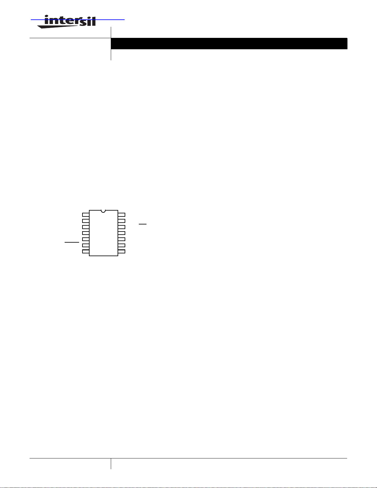
Pinout
ISL12028
(14 LD TSSOP/SOIC)
TOP VIEW
1
X1
X2
NC
NC
NC
RESET
GND
2
NC = No internal connection
14
V
13
3
12
4
11
5
10
6
7
DD
V
BAT
F
/IRQ
OUT
NC
NC
SCL
9
SDA
8
October 18, 2006
Features
• Real Time Clock/Calendar
- Tracks time in Hours, Minutes, and Seconds
- Day of the Week, Day, Month, and Year
- 3 Selectable Frequency Outputs
• Two Non-Volatile Alarms
- Settable on the Second, Minute, Hour, Day of the Week,
Day, or Month
- Repeat Mode (periodic interrupts)
• Automatic Backup to Battery or SuperCap
- Power Failure Detection
- 800nA Battery Supply Current
• On-Chip Oscillator Compensation
- Internal Feedback Resistor and Compensation
Capacitors
- 64 Position Digitally Controlled Trim Capacitor
- 6 Digital Frequency Adjustment Settings to ±30ppm
• 512 x 8 Bits of EEPROM:
- 16-Byte Page Write Mode (32 total pages)
- 8 Modes of Block Lock™ Protection
- Single Byte Write Capability
- Data Retention: 50 years
- Endurance: >2,000,000 Cycles Per Byte
• CPU Supervisor Functions:
- Power On Reset, Low Voltage Sense
- Watchdog Timer (0.25, 0.75, 1.75 sec)
2
C* Interface - 400kHz Data Transfer Rate
•I
• 14 Ld SOIC and 14 Ld TSSOP Packages
• Pb-Free Plus Anneal Available (RoHS Compliant)
Applications
• Utility Meters
• HVAC Equipment
• Audio/Video Components
• Modems
• Network Routers, Hubs, Switches, Bridges
• Cellular Infrastructure Equipment
• Fixed Broadband Wireless Equipment
• Pagers/PDA
• POS Equipment
• Test Meters/Fixtures
• Office Automation (Copiers, Fax)
• Home Appliances
• Computer Products
• Other Industrial/Medical/ Automotive
1
CAUTION: These devices are sensitive to electrostatic discharge; follow proper IC Handling Procedures.
1-888-INTERSIL or 1-888-468-3774
2
*I
C is a Trademark of Philips. Copyright Intersil Americas Inc. 2005-2006. All Rights Reserved
| Intersil (and design) is a registered trademark of Intersil Americas Inc.
All other trademarks mentioned are the property of their respective owners.
ISL12028
Ordering Information
PART NUMBER
(Note) PART MARKING V
RESET
VOLTAGE
ISL12028IB27Z 12028IB27Z 2.63V -40 to +85 14 Ld SOIC M14.15
ISL12028IB27AZ 12028IB27 AZ 2.92V -40 to +85 14 Ld SOIC M14.15
ISL12028IB30AZ 12028IB30 AZ 3.09V -40 to +85 14 Ld SOIC M14.15
ISL12028IBZ 12928IBZ 4.38V -40 to +85 14 Ld SOIC M14.15
ISL12028IBAZ 12028IBAZ 4.64V -40 to +85 14 Ld SOIC M14.15
ISL12028IV27Z 12028 IV27Z 2.63V -40 to +85 14 Ld TSSOP M14.173
ISL12028IV27AZ 12028 27AZ 2.92V -40 to +85 14 Ld TSSOP M14.173
ISL12028IV30AZ 12028 30AZ 3.09V -40 to +85 14 Ld TSSOP M14.173
ISL12028IVZ 12028 IVZ 4.38V -40 to +85 14 Ld TSSOP M14.173
ISL12028IVAZ 12028 IVAZ 4.64V -40 to +85 14 Ld TSSOP M14.173
NOTE: Intersil Pb-free plus anneal products employ special Pb-free material sets; molding compounds/die attach materials and 100% matte tin plate
termination finish, which are RoHS compliant and compatible with both SnPb and Pb-free soldering operations. Intersil Pb-free products are MSL
classified at Pb-free peak reflow temperatures that meet or exceed the Pb-free requirements of IPC/JEDEC J STD-020.
Tape & Reel - add “-T” suffix after the part number.
TEMP RANGE
(°C)
PACKAGE
(Pb-free) PKG. DWG. #
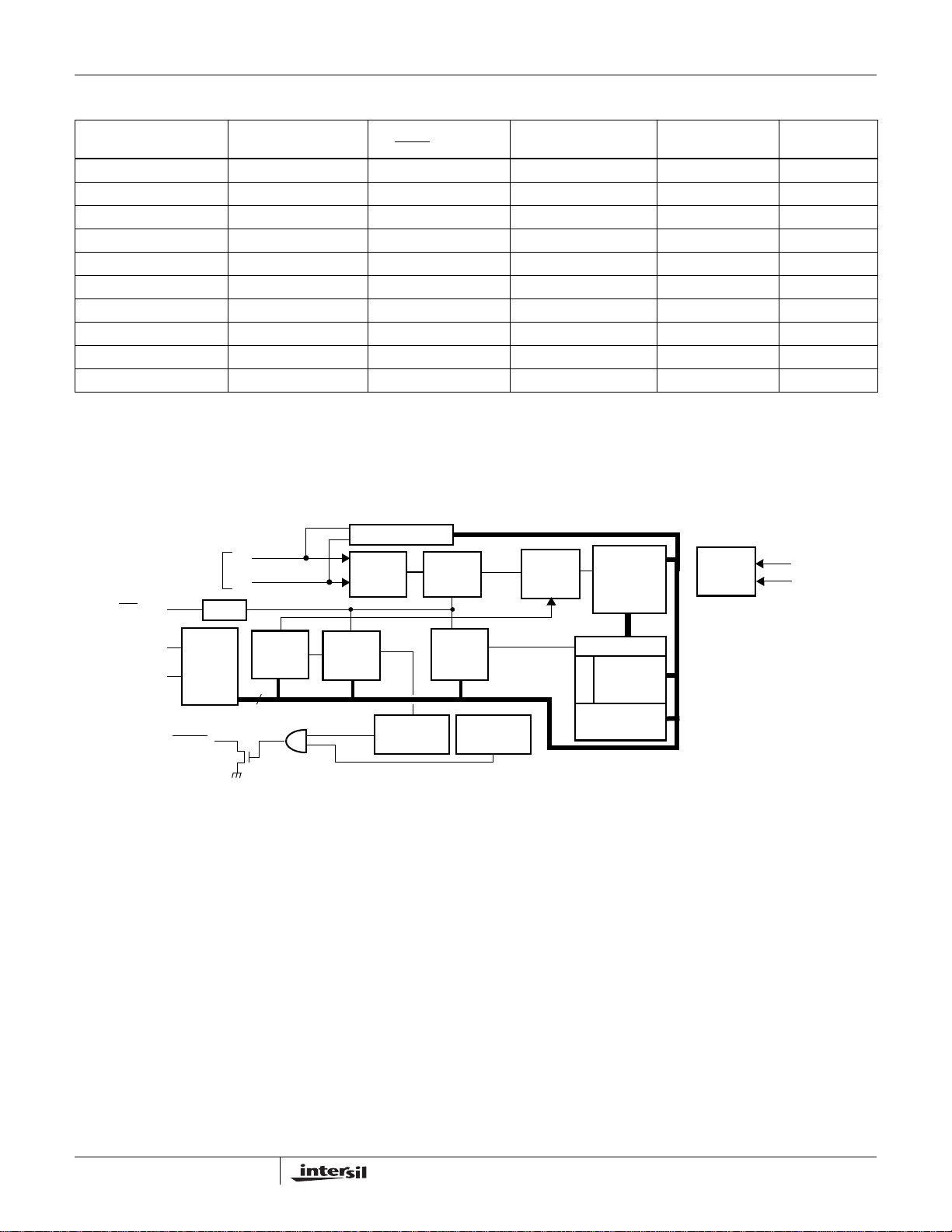
Block Diagram
IRQ/F
OUT
SCL
SDA
32.768kHz
Serial
Interface
Decoder
RESET
Select
OSC Compensation
X1
X2
Control
Decode
Logic
Oscillator
Control/
Registers
(EEPROM)
Frequency
Divider
Status
Registers
(SRAM)
1Hz
8
Watchdog
Timer
Low Voltage
Reset
Timer
Calendar
Logic
Alarm
Compare
Alarm Regs
Mask
EEPROM
Time
Keeping
Registers
(SRAM)
(EEPROM)
4K
ARRAY
Battery
Switch
Circuitry
V
V
DD
BACK
2
FN8233.5
October 18, 2006
ISL12028
Pin Descriptions
PIN
NUMBER SYMBOL DESCRIPTION
1 X1 The X1 pin is the input of an inverting amplifier and is intended to be connected to one pin of an external 32.768kHz
2 X2 The X2 pin is the output of an inverting amplifier and is intended to be connected to one pin of an external 32.768kHz
6 RESET
7 GND Ground.
8 S DA Serial Data (SDA) is a bidirectional pin used to transfer serial data into and out of the device. It has an open drain
9 SCL The Serial Clock (SCL) input is used to clock all serial data into and out of the device. The input buffer on this pin is
12
13 V
14 V
3, 4, 5, 10,
11
IRQ/F
BAT
DD
N.C. No Internal Connection.
quartz crystal.
quartz crystal.
RESET. This is a reset signal output. This signal notifies a host processor that the “watchdog” time period has
expired or that the voltage has dropped below a fixed V
Recommended value for the pull-up resistor is 5kΩ, If unused, connect to ground.
output and may be wire OR’ed with other open drain or open collector outputs.
always active (not gated).
Interrupt Output/Frequency Output is a multi-functional pin that can be used as interrupt or frequency output pin. The
OUT
function is set via the configuration register.
This input provides a backup supply voltage to the device. V
V
supply fails. This pin should be tied to ground if not used.
DD
Power Supply.
threshold. It is an open drain active LOW output.
TRIP
supplies power to the device in the event that the
BAT
3
FN8233.5
October 18, 2006
ISL12028
Absolute Maximum Ratings Thermal Information
Voltage on VDD, V
(respect to ground). . . . . . . . . . . . . . . . . . . . . . . . . . -0.3V to 6.0V
, SCL, SDA, RESET and IRQ/F
BAT
OUT
Pins
Voltage on X1 and X2 Pins
(respect to ground). . . . . . . . . . . . . . . . . . . . . . . . . . -0.3V to 2.5V
Latchup (Note 1) . . . . . . . . . . . . . . . . . . .Class II, Level B @ +85°C
ESD Rating (MIL-STD-883, Method 3014) . . . . . . . . . . . . . . .>±2kV
ESD Rating (Machine Model) . . . . . . . . . . . . . . . . . . . . . . . . .>175V
CAUTION: Stresses above those listed in “Absolute Maximum Ratings” may cause permanent damage to the device. This is a stress only rating and operation of the
device at these or any other conditions above those indicated in the operational sections of this specification is not implied.
NOTES:
1. Jedec Class II pulse conditions and failure criterion used. Level B exceptions are: Using a max positive pulse of 8.35V on all pins except X1 and
X2, Using a max positive pulse of 2.75V on X1 and X2, and using a max negative pulse of -1V for all pins.
is measured with the component mounted on a high effective thermal conductivity test board in free air. See Tech Brief TB379 for details.
2. θ
JA
DC Operating Characteristics
Unless otherwise noted, V
SYMBOL PARAMETER CONDITIONS MIN TYP MAX UNIT NOTES
V
V
BAT
Main Power Supply 2.7 5.5 V
DD
Backup Power Supply 1.8 5.5 V
= +2.7V to +5.5V, TA = -40°C to +85°C, Typical values are at TA = +25°C and V
DD
Thermal Resistance (Note 2) θ
(°C/W)
JA
14 Ld SOIC Package . . . . . . . . . . . . . . . . . . . . . . . . 100
14 Ld TSSOP Package . . . . . . . . . . . . . . . . . . . . . . 110
Storage Temperature. . . . . . . . . . . . . . . . . . . . . . . .- 65°C to +150°C
Lead Temperature (Soldering, 10s). . . . . . . . . . . . . . . . . . . .+300°C
= 3.3V
DD
Electrical Specifications
SYMBOL PARAMETER CONDITIONS MIN TYP MAX UNIT NOTES
I
DD1
I
DD2
I
DD3
I
BAT
I
BATLKG
V
TRIP
V
TRIPHYSVTRIP
V
BATHYSVBAT
V
DD SR-VDD
IRQ
/F
V
RESET
I
LO
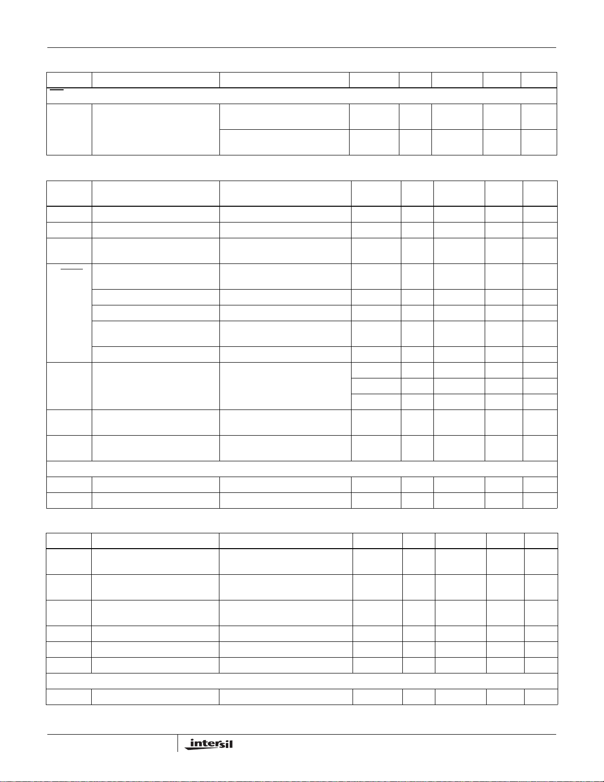
Supply Current with I2C Active VDD = 2.7V 500 µA 3, 4, 5
VDD = 5.5V 800 µA
Supply Current for Non-Volatile
Programming
Supply Current for Main
Timekeeping (Low Power Mode)
Battery Supply Current V
Battery Input Leakage VDD = 5.5V, V
V
Mode Threshold 1.8 2.2 2.6 V 7
BAT
VDD = 2.7V 2.5 mA 3, 4, 5
VDD = 5.5V 3.5 mA
VDD = V
V
DD
BAT
V
DD
V
BAT
V
DD
SDA
= V
SDA
= 1.8V,
= V
SDA
= 3.0V,
= V
SDA
= V
= 2.7V 10 µA 5
SCL
= V
= 5.5V 20 µA
SCL
800 1000 nA 3, 6, 7
= V
SCL
= V
RESET
= 0V
850 1200 nA
= V
= V
SCL
= 1.8V 100 nA
BAT
RESET
= 0V
Hysteresis 30 mV 7, 9
Hysteresis 50 mV 7, 9
Negative Slew Rate 10 V/ms 8
RESET OUTPUTS
OUT,
Output Low Voltage VDD = 5.5V
OL
I
OL
V
DD
I
OL
= 3mA
= 2.7V
= 1mA
0.3*V
0.3*V
DD
DD
OUTPUT
Output Leakage Current VDD = 5.5V
V
= 5.5V
OUT
100 400 nA
, 3
V
V
4
FN8233.5
October 18, 2006
ISL12028
Electrical Specifications (Continued)
SYMBOL PARAMETER CONDITIONS MIN TYP MAX UNIT NOTES
IRQ/F
Watchdog Timer/Low Voltage Reset Parameters
SYMBOL PARAMETER CONDITIONS MIN
t
V
V
EEPROM SPECIFICATIONS
OUT,
V
OH
t
RPD
PURST
RVALID
RESET
t
WDO
t
RST
t
RSP
OUTPUT
Output High Voltage VDD = 5.5V
I
= -1.0mA
OL
V
= 2.7V
DD
I
= -0.4mA
OL
x 0.7 V
V
DD
x 0.7 V
V
DD
TYP
(Note 5) MAX UNITS NOTES
VDD Detect to RESET LOW 500 ns 9
Power Up Reset Time-Out Delay 100 250 400 ms
Minimum VDD for Valid RESET
1.0 V
Output
ISL12028-4.5A Reset Voltage
4.59 4.64 4.69 V
Level
ISL12028 Reset Voltage Level 4.33 4.38 4.43 V
ISL12028-3 Reset Voltage Level 3.04 3.09 3.14 V
ISL12028-2.7A Reset Voltage
2.87 2.92 2.97 V
Level
ISL12028-2.7 Reset Voltage Level 2.58 2.63 2.68 V
Watchdog Timer Period 32.768kHz crystal between X1 and
X2
1.70 1.75 1.801 s
725 750 775 ms
225 250 275 ms
Watchdog Timer Reset Time-Out
Delay
I2C Interface Minimum Restart
32.768kHz crystal between X1 and
X2
225 250 275 ms
1.2 µs
Time
EEPROM Endurance >2,000,000 Cycles
EEPROM Retention Temperature ≤ +75°C 50 Years
Serial Interface (I2C) Specifications
SYMBOL PARAMETER CONDITIONS MIN TYP MAX UNITS NOTES
V
V
Hysteresis SDA and SCL Input Buffer
V
I
I
LO
TIMING CHARACTERISTICS
f
SCL
SDA, and SCL Input Buffer LOW
IL
SBIB = 1 (Under VDD mode) -0.3 0.3 x V
Voltage
SDA, and SCL Input Buffer HIGH
IH
Voltage
Hysteresis
SDA Output Buffer LOW Voltage I
OL
Input Leakage Current on SCL V
LI
I/O Leakage Current on SDA V
SBIB = 1 (Under VDD mode) 0.7 x V
SBIB = 1 (Under V
= 4mA 0 0.4 V
OL
= 5.5V 0.1 10 µA
IN
= 5.5V 0.1 10 µA
IN
mode) 0.05 x V
DD
DD
DD
VDD + 0.3 V
SCL Frequency 400 kHz
5
DD
V
V
FN8233.5
October 18, 2006

ISL12028
Serial Interface (I2C) Specifications (Continued)
SYMBOL PARAMETER CONDITIONS MIN TYP MAX UNITS NOTES
t
t
AA
t
BUF
t
LOW
t
HIGH
t
SU:STA
t
HD:STA
t
SU:DAT
t
HD:DAT
t
SU:STO
t
HD:STO
t
DH
t
Cb Capacitive Loading of SDA or SCL Total on-chip and off-chip 10 400 pF
Cpin SDA, and SCL Pin Capacitance 10 pF
t
WC
NOTES:
3. IRQ/
4. V
5. V
6. Bit BSW = 0 (Standard Mode), V
7. Specified at +25°C.
8. In order to ensure proper timekeeping, the V
9. Parameter is not 100% tested.
10. t
WC
sequence of a serial interface Write operation, to the end of the self-timed internal non-volatile write cycle.
Pulse width Suppression Time at
IN
SDA and SCL Inputs
SCL Falling Edge to SDA Output
Data Valid
Time the bus must be free before
the start of a new transmission
Any pulse narrower than the max
spec is suppressed.
SCL falling edge crossing 30% of
V
, until SDA exits the 30% to 70%
DD
of V
window.
DD
SDA crossing 70% of VDD during a
STOP condition, to SDA crossing
70% of V
during the following
DD
50 ns
900 ns
1300 ns
START condition.
Clock LOW Time Measured at the 30% of VDD
1300 ns
crossing.
Clock HIGH Time Measured at the 70% of VDD
600 ns
crossing.
START Condition Setup Time SCL rising edge to SDA falling edge.
Both crossing 70% of V
STAR T Condition Hold Time From SDA falling edge crossing 30%
of V
to SCL falling edge crossing
DD
70% of V
DD
.
Input Data Setup Time From SDA exiting the 30% to 70% of
V
window, to SCL rising edge
DD
crossing 30% of V
DD
Input Data Hold Time From SCL falling edge crossing 70%
of V
to SDA entering the 30% to
DD
70% of V
window.
DD
STOP Condition Setup Time From SCL rising edge crossing 70%
of V
, to SDA rising edge crossing
DD
STOP Condition Hold Time for
Read, or Volatile Only Write
30% of V
From SDA rising edge to SCL falling
edge. Both crossing 70% of V
DD
.
Output Data Hold Time From SCL falling edge crossing 30%
of V
, until SDA enters the 30% to
DD
70% of V
SDA and SCL Rise Time From 30% to 70% of V
R
window.
DD
DD
DD
.
.
DD
600 ns
600 ns
100 ns
0ns
600 ns
600 ns
0ns
20 +
250 ns
0.1 x Cb
t
SDA and SCL Fall Time From 70% to 30% of V
F
DD
20 +
0.1 x Cb
250 ns
Non-volatile Write Cycle Time 12 20 ms 10
F
Inactive (no frequency output and no alarms).
OUT
= VDD x 0.1, V
IL
= 2.63V (VDD must be greater than V
RESET
= VDD x 0.9, f
IH
SCL
BAT
= 400kHz.
≥ 1.8V.
), V
RESET
DD SR-
= 0V.
BAT
specification must be followed.
is the minimum cycle time to be allowed for any non-volatile Write by the user, it is the time from valid STOP condition at the end of Write
6
FN8233.5
October 18, 2006
Timing Diagrams
ISL12028
SCL
SDA
(INPUT TIMING)
SDA
(OUTPUT TIMING)
SCL
SDA
t
F
t
SU:DAT
t
SU:STA
t
HD:STA
8TH BIT OF LAST BYTE ACK
t
HIGH
t
LOW
t
HD:DAT
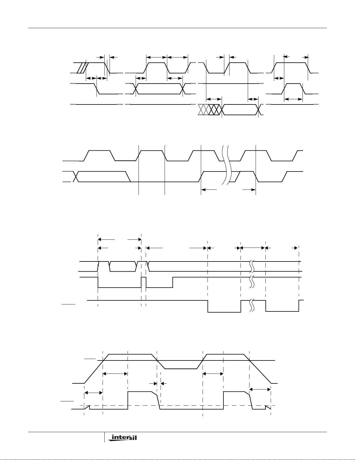
FIGURE 1. BUS TIMING
STOP
CONDITION
FIGURE 2. WRITE CYCLE TIMING
t
R
t
DH
t
AA
t
WC
t
BUF
t
HD:STO
t
SU:STO
START
CONDITION
SCL
SDA
RESET
V
RESET
DD
t
RSP
t
RSP<tWDO
START STOP START
Note: All inputs are ignored during the active reset period (t
V
RESET
t
PURST
t
R
t
RSP>tWDO
FIGURE 3. WATCHDOG TIMING
t
t
RPD
PURST
t
RST
RST
).
t
RSP>tWDO
t
RST
t
F
V
RVALID
FIGURE 4. RESET TIMING
7
FN8233.5
October 18, 2006
ISL12028
Typical Performance Curves Temperature is 25°C unless otherwise specified
0.90
4.00
3.50
3.00
2.50
2.00
Ibat (uA)
1.50
1.00
0.50
0.00
1.8 2.3 2.8 3.3 3.8 4.3 4.8 5.3
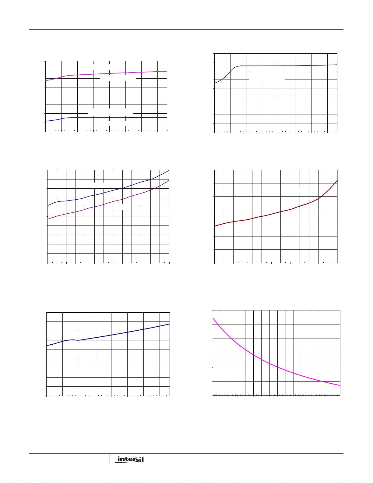
FIGURE 5. I
BSW = 0 or 1
SCL,SDA pullups = 0V
SCL,SDA pullups = Vbat
BSW = 0 or 1
Vbat (V)
vs V
BAT
BAT,
SBIB = 0 FIGURE 6. I
0.80
0.70
0.60
0.50
Ibat
0.40
0.30
0.20
0.10
0.00
1.80 2.30 2.80 3.30 3.80 4.30 4.80 5.30
SCL,SDA pullups = 0V
BSW = 0 or 1
Vbat(V)
vs V
BAT
BAT,
SBIB = 1
5.00
4.50
4.00
3.50
3.00
2.50
Idd (uA)
2.00
1.50
1.00
0.50
0.00
-45-35-25-15-5 51525354555657585
Vdd=5.5V
Vdd=3.3V
Temperature
FIGURE 7. I
4.50
4.00
3.50
3.00
2.50
2.00
Idd (uA)
1.50
1.00
0.50
0.00
1.8 2.3 2.8 3.3 3.8 4.3 4.8 5.3
vs TEMPERATURE FIGURE 8. I
DD3
Vdd (V)
FIGURE 9. I
DD3
vs V
DD
1.40
1.20
Vbat = 3.0V
1.00
0.80
0.60
Ibat (uA)
0.40
0.20
0.00
-45-35-25-15-5 5 1525354555657585
Temperature
vs TEMPERATURE
BAT
80
60
40
20
0
PPM change from ATR=0
-20
-40
-32 -28 -24 -20 -16 -1 2 -8 -4 0 4 8 12 16 20 24 28
ATR setting
FIGURE 10. ∆F
vs ATR SETTING
OUT
8
FN8233.5
October 18, 2006

ISL12028
Description
The ISL12028 device is a Real Time Clock with clock/
calendar, two polled alarms with integrated 512x8 EEPROM,
oscillator compensation, CPU Supervisor (Power on Reset,
Low Voltage Sensing and Watchdog T imer) and battery
backup switch.
The oscillator uses an external, low-cost 32.768kHz crystal.
All compensation and trim components are integrated on the
chip. This eliminates several external discrete components
and a trim capacitor, saving board area and component cost.
The Real-Time Clock keeps track of time with separate
registers for Hours, Minutes, Seconds. The Calendar has
separate registers for Date, Month, Year and Day-of-week.
The calendar is correct through 2099, with automatic leap
year correction.
The Dual Alarms can be set to any Clock/Calendar value for
a match. For instance, every minute, every Tuesday, or 5:23
AM on March 21. The alarms can be polled in the Status
Register or can provide a hardware interrupt (IRQ
/F
OUT
Pin). There is a repeat mode for the alarms allowing a
periodic interrupt.
The IRQ
/F
pin may be software selected to provide a
OUT
frequency output of 1Hz, 4096Hz, or 32,768Hz or inactive.
The ISL12028 device integrates CPU Supervisory functions
(POR, WDT) and Battery Switch. There is Power-On-Reset
(RESET
V
will also assert RESET
V
) output with 250ms delay from power on when the
supply crosses the V
DD
when V
threshold for the device. The V
RESET
threshold for the device. It
RESET
goes below the specified
DD
RESET
threshold is
selectable via VTS2/VTS1/VTS0 registers to five (5) preselected levels. There is WatchDog Timer (WDT) with 3
selectable time-out periods (0.25s, 0.75s and 1.75s) and
disabled setting. The WatchDog Timer activates the RESET
pin when it expires. Normally, the I
when the RESET
output is active, but this can be changed
by using a register bit to enable I
2
C Interface is disabled
2
C operation in battery
backup mode.
The device offers a backup power input pin. This V
BAT
pin
allows the device to be backed up by battery or SuperCap.
The entire ISL12028 device is fully operational from 2.7 to
5.5V and the clock/calendar portion of the ISL12028 device
remains fully operational down to 1.8V (Standby Mode).
The ISL12028 device provides 4k bits of EEPROM with 8
modes of BlockLock™ control. The BlockLock allows a safe,
secure memory for critical user and configuration data, while
allowing a large user storage area.
Pin Descriptions
Serial Clock (SCL)
The SCL input is used to clock all data into and out of the
device. The input buffer on this pin is always active (not
gated). The pull-up resistor on this pin must use the same
voltage source as V
DD
.
Serial Data (SDA)
SDA is a bidirectional pin used to transfer data into and out
of the device. It has an open drain output and may be wire
ORed with other open drain or open collector outputs. The
input buffer is always active (not gated).
This open drain output requires the use of a pull-up resistor.
The pull-up resistor on this pin must use the same voltage
source as V
. The output circuitry controls the fall time of
DD
the output signal with the use of a slope controlled pulldown. The circuit is designed for 400kHz I
2
C interface
speed.
V
BAT
This input provides a backup supply voltage to the device.
V
supplies power to the device in the event the VDD
BAT
supply fails. This pin can be connected to a battery, a
SuperCap or tied to ground if not used.
IRQ/F
(Interrupt Output/Frequency Output)
OUT
This dual function pin can be used as an interrupt or
frequency output pin. The IRQ
/F
mode is selected via
OUT
the frequency out control bits of the control/status register.
• Interrupt Mode. The pin provides an interrupt signal
output. This signal notifies a host processor that an alarm
has occurred and requests action. It is an open drain
active low output.
• Frequency Output Mode. The pin outputs a clock signal
which is related to the crystal frequency. The frequency
output is user selectable and enabled via the I
2
C bus. It is
an open drain output.
RESET
The RESET signal output can be used to notify a host
processor that the watchdog timer has expired or the V
voltage supply has dipped below the V
threshold. It is
RESET
DD
an open drain, active LOW output. Recommended value for
the pull-up resistor is 10kΩ. If unused it can be tied to
ground.
X1, X2
The X1 and X2 pins are the input and output, respectively, of
an inverting amplifier. An external 32.768kHz quartz crystal
is used with the ISL12028 to supply a timebase for the real
time clock. Internal compensation circuitry provides high
accuracy over the operating temperature range from
-40°C to +85°C. This oscillator compensation network can
be used to calibrate the crystal timing accuracy over
temperature either during manufacturing or with an external
temperature sensor and microcontroller for active
compensation. X2 is intended to drive a crystal only, and
should not drive any external circuit.
9
FN8233.5
October 18, 2006
 Loading...