

Page 1
INTERSIL
IM6100
CMOS
MICROPROCESSOR
12
BIT
D
Page 2
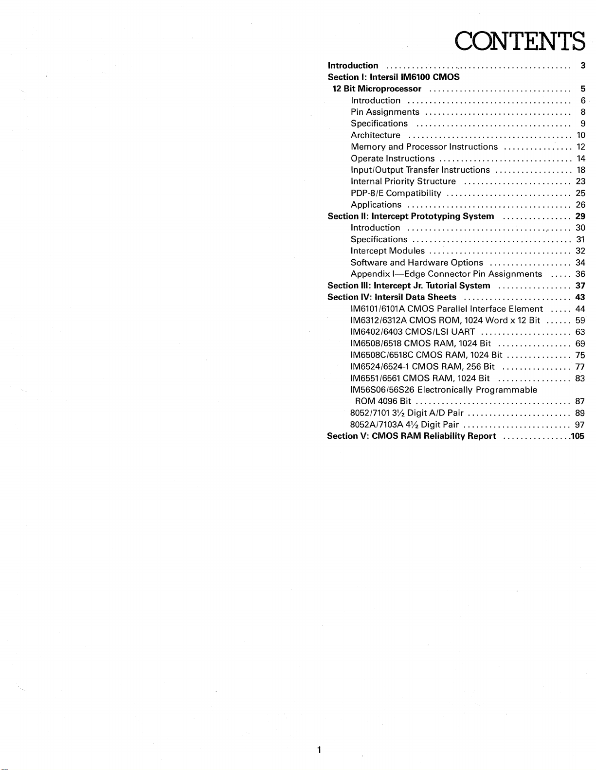
CONTENTS
Introduction
Section
12
Section
Section
Section
Section V:
I:
IntersillM6100
Bit Microprocessor
Introduction
Pin
Assignments
Specifications
Architecture
Memory
Operate
Input/Output
Internal
PDP-8/E
Applications
II: Intercept Prototyping System
Introduction
Specifications
Intercept
Software
Appendix
III: Intercept
IV: Intersil Data Sheets
IM6101/6101A
IM6312/6312A
IM6402/6403
IM6508/6518
IM6508C/6518C
IM6524/6524-1
IM6551
16561
IM56S06/56S26
ROM 4096
8052/7101
8052A/7103A
CMOS RAM Reliability Report
............................................
CMOS
.................................
......................................
..................................
....................................
......................................
and Processor
Instructions
Transfer
Priority
Compatibility
Structure
......................................
.........................
.....................................
Modules
and
Hardware
I-Edge
Jr.
CMOS
CMOS
CMOS/LSI UART
CMOS
CMOS RAM, 1024
CMOS RAM, 256
CMOS
Electronically
Bit
....................................
31;2
Digit
41;2
Instructions
...............................
Instructions
.........................
.............................
.................................
Options
Connector
Tutorial System
.........................
Parallel Interface
ROM, 1024
RAM, 1024
RAM, 1024 Bit
AID
Pair
Digit
Pair
.........................
..................
...................
Pin
Assignments
.................
Word x 12
.....................
Bit
.................
Bit
Bit
.................
Programmable
........................
................
................
~
.....
Element
Bit
...............
................
...............
'.' . . .
.....
.....
......
..
. 105
3
5
6
8
9
10
12
14
18
23
25
26
29
30
31
32
34
36
37
43
44
59
63
69
75
77
83
87
89
97
1
Page 3

2
Page 4
INTRODUCTION
Since its
become a company
In
this
publication,
advanced linear
bipolar, MOS, metal-gate CMOS
all
are
advantage
thinking
technologies
performance
developed
lntersil over
resulting in packing densities which surpass
metal gate process
proved 2: 1.
process,
RAMs, has lead
microprocessor.
length, parallel
plement
of
internal
at
Two
el
The
external
instruction
supply
The
nal
and peripheral devices.
represented
The
Mass
The
Digital
circuitry
any
speed
pins are available
iminating
crystal can be removed and
and
device design
components
founding
of
addition
that,
company,
product.
through
arithmetic.
clock
to
lntersil has developed
products
in lntersil's line,
because
many
produced
and
greater
Silicon
IM6100
Equipment
Gate
two
years ago, offers a
3:
production
previously
to
and
transfer
is
between
the
need
generator. A 12-bit
is
performed
in
2.5psec
is
required
on
July
26,
1967,
many
products
the
digital CMOS devices
and
they
were developed
of
the
by lntersil will
efficiency and flexibility
CMOS process, which was
1.
Additionally,
experience
announced
the
practicality
IM6100A are single address,
microprocessors using 12-bit,
The
processors recognize
Corporation's
completely
DC
and
the
to
allow
for
clock
in 5psec
by
the
optimized
for
and processes.
and
semiconductor
and
silicon-gate CMOS processes
with
the
different
with
static
maximum
for
generators
the
by
IM6100A
to
minimize
interfacing
kinds
work
together
semiconductor
circuit
the
256
of
introducing
PDP8/E
and
is
operating
an
external
and
processor
memory-accumulator
the
IM6100 using a
using a
the
with
lntersil, Inc. has
covered
markets
by
performance
Silicon
and
the
minicomputer.
designed
in
a line
memories.
significant
a single
of
devices
for
enhanced
of
developed
structure
the
conventional
Gate
1024
bit
the
fixed
two's
instruction
to
frequency.
crystal
level
translators.
clocked
+10
volt
number
standard
detail
forward-
the
of
memory
in
of
TTL
design
and
final
at
is
im-
CMOS
CMOS
IM6100
word
com-
set
The
operate
thereby
by an
ADD
+5
volt
supply.
exter-
described
product.
reserves
circuitry
in
this
3
lntersil
cannot
other
No
other
the
right
and
document.
assume responsibility
than
circuitry
circuit
to
change
specifications
entirely
patent
without
of
any
for
use
of
any
circuitry
embodied
licenses are implied. lntersil
notice
I ntersil
at
product
in
an lntersil
any
time
represented
the
Page 5

4
Page 6

SECTION
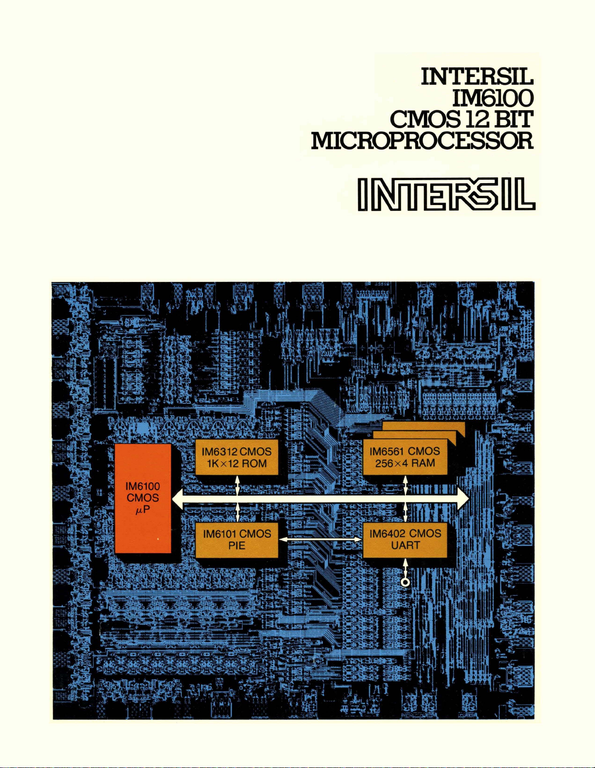
INTERSIL
IM6100
I:
CMOS
12
BIT
MICROPROCESSOR
5
Page 7

INTRODUCTION
IM6100
Since its founding on July 26, 1967, INTERSIL INC. has offered
its customers advanced products utilizing the semiconductor industry's most
ture of
in 1972, offers a semiconductor structure resulting in packing densities which surpass the
tionally, circuit performance is improved 2:1.
ess, through
has
technologically sophisticated processes for the manufac-
practical, economical devices.
The Silicon Gate
Mass production experience with the
lead to the practicality of introducing the IM6100 microprocessor.
MICROPROCESSOR
CMOS process, which was developed at Intersil
conventional metal gate process 3:1. Addi-
Silicon Gate CMOS proc-
previously announced 256 and 1024 bit CMOS RAMs,
The IM6100 is a single address, fixed word length, parallel transfer microprocessor using 12-bit, two's
processors recognize the instruction set of
ration's PDP8/E minicomputer. The
static and is designed to operate at any speed between DC and the
maximum operating frequency.
external crystal thereby eliminating the need for clock generators
and
level translators. The crystal can be removed and the processor
clocked
accumulator ADD instruction, using a + 5 volt supply, is performed in
5p,sec by the IM6100, in 6p,sec by the IM6100C and in 2.5p,sec by the
IM6100A using a +10 volt supply. The device design is optimized to
minimize the number of
with standard memory and
by
an
external
Two
clock
external components required for interfacing
peripheral devices.
complement arithmetic. The
Digital Equipment Corpo-
internal circuitry is completely
pins are available to allow for an
generator. A 12-bit
memory-
6
Page 8

FEATURES
APPLICATIONS
DESIGN
o Silicon Gate Complementary MOS
o Fully Static-O to 8 MHz
o Single Power Supply
IM6100/C
IM6100A
o Crystal Controlled
o Low Power Dissipation <
o Single Power Supply 4V
o TTL Compatible at 5 Volts
o Excellent Noise Immunity
o
-55°C
INTERFACE
o
Memory-Any
o Control Panel
o Switch Register
o Asynchronous
Communication
o 64 I/O Devices with PDP-8/E Compatible Interface
o Device Controlled Input-Output
o All Control Signals Produced By The CPU
o Power-on Initialize
ARCHITECTURAL
o Executes PDP-8/E, Instruction Set
o Direct, Indirect, and Autoindexed Memory Addressing
o 12-Bit Memory Accumulator ADD Instruction
IM6100 5fLsec
IM6100A 2.5fLsec @ +10 volts/8.0 MHz
IM6100C 6fLsec @
o
Input-Output Instruction
IM6100 8.5fLsec
IM6100A 4.25fLseC @ +10 volts/8 MHz
IM6100C 10.2fLsec @
o Single-Clock, Single-Instruction Capability
o Direct Memory Access (DMA)
o Interrupt
o Dedicated Control Panel Features
Vee=5
volts
Vee=10
to +125°C Operation
volts
On
Chip Timing
10
~
Speed
CPU-Memory
@
+5
+5
@
+5
+5
mW @ 4 MHz @ 5 volts
Vee ~ 11V
and
CPU-Device
volts/4.0 MHz
volts/3.3 MHz
volts/4.0 MHz
volts/3.3 MHz
o Intelligent Computer Terminals
o POS Terminals
o Portable Terminals
o Aerospace/Satellite System
o Automotive Systems
o Remote Data Acquisition Systems
o Process Control
o Instrumentation
o Medical Electronics
o Displays
o Traffic Control
o Navigation
7
Page 9
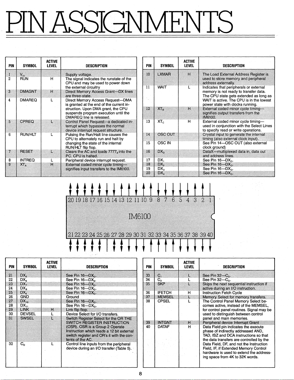
PIN
ASSIGNMENTS
;',
,',
<',
Data Field pin
phase
TAD,
the data transfers are controlled by the
Data
Field,
hardware is used to extend the address-
ing space from
,
of.
indirectly addressed AND,
ISZ and DCA instructions so that
Field,
DF,
IF,
and not the Instruction
if
Extended Memory Control
4K
to
32K
words.
Page 10
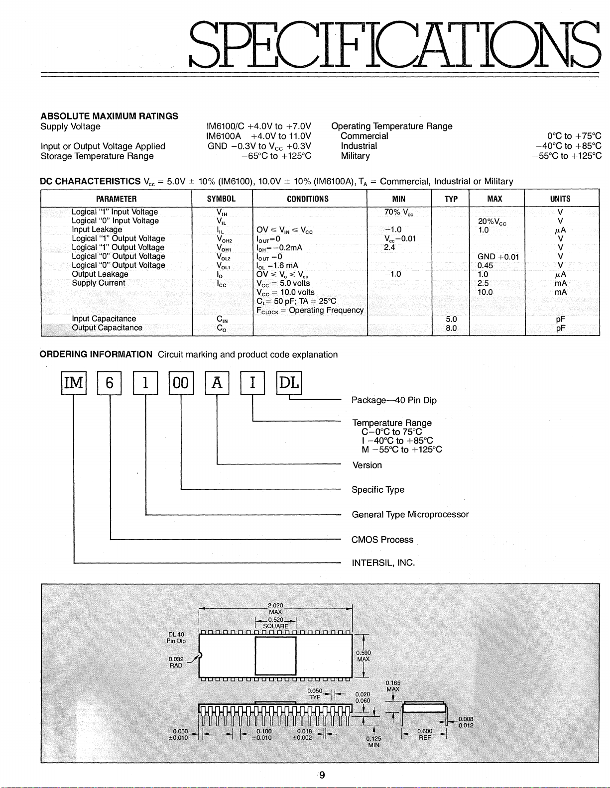
ABSOLUTE MAXIMUM RATINGS
Supply Voltage
or Output Voltage Applied
Input
Storage Temperature Range
DC
CHARACTERISTICS
Vee
= 5.0V ±
SPECIFICATIONS
IM6100/C +4.0V to +7.0V
IM6100A +4.0V
GND
-0.3V
-65°C
10%
(IM6100), 10.0V ± 10% (IM6100A),
to 11.0V
to
Vee
to +125°C
+0.3V
Operating Temperature Range
Commercial
Industrial
Military
TA
= Commercial, Industrial or Military
O°C
-40°C
-55°C
to +75°C
to +85°C
to +125°C
PARAMETER
Logical "1" Input Voltage V
Logical
"0"
Input Leakage
Logical "1" Output Voltage
Logical "1" Output Voltage
Logical
Logical
Output Leakage
Supply Current
Input Capacitance
Output Capacitance
.".
Input Voltage
"0"
Output Voltage
"0"
Output Voltage
SYMBOL
IH
V
IL
IlL
V
OH2
V
OH1
V
OL2
V
OL1
10
lec
C
IN
Co
CONDITIONS
OV ~ VIN ~ Vee
10ur=0
IOH=-0.2mA
lour
=0
10L
=1.6
OV ~ V
Vee
Vee
CL= 50 pF;
F
mA
~
Vee
o
= 5.0 volts
= 10.0 volts
TA
= Operating Frequency
eLDeK
= 25°C
ORDERING INFORMATION Circuit marking and product code explanation
MIN
70%
Vee
-1.0
O
01
Vee-
.
2.4
-1.0
Package-40
Pin Dip
Temperature Range
C-O°C
I
M
-40°C
-55°C
to 75°C
to +85°C
to +125°C
Version
TYP
5.0
8.0
MAX
20%V
ee
1.0
GND +0.01
0.45
1.0
2.5
10.0
UNITS
V
V
/LA
V
V
V
V
p,A
mA
mA
pF
pF
Specific
Type
General Type Microprocessor
CMOS Process
INTERSIL, INC.
9
Page 11
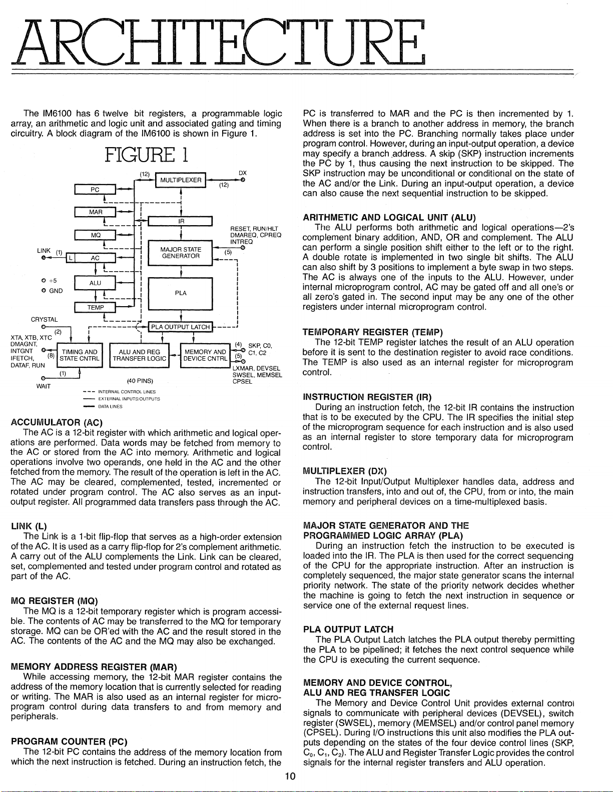
ARCHITECTURE
The IM6100 has 6 twelve bit registers, a programmable logic
array, an arithmetic and logic unit and associated gating and timing
circuitry. A
XTA,
XTB, XTC
DMAGNT,
INTGNT
IFETCH,
DATAF,
block diagram of the IM6100 is shown
FIGURE
LINK
(1)
,......,.
___
-,
in
1
~L.;;L;.J..I_:..:r_~
o +5
()
GND
CRYSTAL
(2)
,....--'----.1.--,
RUN
WAIT
....-_--1_--1...,
(40 PINS)
- - - INTERNAL CONTROL LINES
- EXTEHNAL INPUTS/OUTPUTS
- DATA
LINES
Figure
DX
(12)
RESET, RUN/HLT
DMAREQ,CPREO
INTREQ
(5)
---.,
I
I
I
I
I
I
I
I
I
I
I
I
I
____
J
1.
SKP,
C1,
C2
CO,
ACCUMULATOR (AC)
The AC is a 12-bit register with which arithmetic and logical oper-
ations are performed. Data words may be fetched from memory to
the AC or stored from the AC into memory. Arithmetic and
operations involve two operands, one held in the
fetched from the memory. The
The AC may
be
cleared, complemented, tested, incremented or
rotated under program
output register.
All programmed data transfers pass through the
result of the operation
control. The AC also serves
AC
is
logical
and the other
left
in
the AC.
as
an
input-
AC,
PC
is transferred to MAR and the
When there
address
program
is
a branch to another address
is
set into the
PC.
Branching normally takes place under
control. However, during
may specify a branch .address. A skip
the
PC
by
1,
SKP instruction may
thus causing the next instruction to
be
unconditional or conditional
the AC and/or the Link. During
can
also cause the next sequential instruction to be skipped.
PC
is then incremented by
in
memory, the branch
an
input-output operation, a device
(SKP) instruction increments
be
skipped. The
on
the state of
an
input-output operation, a device
ARITHMETIC AND LOGICAL UNIT (ALU)
The ALU performs both arithmetic and logical
operations-2's
complement binary addition, AND, OR and complement. The ALU
can perform a
A
double rotate
can
also shift
The AC is
single position shift either to the left or to the right.
is
implemented
by
3 positions to implement a byte swap
in
two single bit shifts. The ALU
in
two steps.
always one of the inputs to the ALU. However, under
internal microprogram control, AC may be gated off and all one's or
all zero's gated
registers under
TEMPORARY REGISTER
The 12-bit TEMP register
before it
is
The TEMP is
in,
The second input may
be
anyone
of the other
internal microprogram control.
(TEMP)
latches the result of
an
ALU operation
sent to the destination register to avoid race conditions.
also used
as
an
internal register for microprogram
control.
INSTRUCTION REGISTER (IR)
During an instruction fetch, the 12-bit
that
is
to
be
executed by the CPU. The
of the microprogram sequence for each instruction and
as
an
internal register to store temporary data for microprogram
IR
contains the instruction
IR
specifies the initial step
is
also used
control.
MULTIPLEXER (DX)
The 12-bit Input/Output Multiplexer handles data, address and
instruction transfers, into and out of, the CPU, from or into, the main
memory and
peripheral devices
on
a time-multiplexed basis.
1.
LINK (L)
is
The Link
of the AC.
a 1-bit flip-flop that serves
It
is used
as
a carry flip-flop for 2's complement arithmetic.
A carry out of the ALU complements the Link. Link can
as
a high-order extension
be
cleared,
set, complemented and tested under program control and rotated as
part of the AC.
MQ
REGISTER (MQ)
MQ
The
ble. The contents of AC may
storage.
AC.
is a 12-bit temporary register which
be
transferred to the
MQ
can
be
OR'ed with the AC and the result stored
The contents of the AC and the MQ may also
is
program accessi-
MQ
for temporary
be
exchanged.
in
the
MEMORY ADDRESS REGISTER (MAR)
While accessing memory, the 12-bit MAR register contains the
address of the memory
or writing. The MAR is
program
control during data transfers to and from memory and
location that is currently selected for reading
also used
as
an
internal register for micro-
peripherals.
PROGRAM COUNTER (PC)
PC
The 12-bit
which the next instruction
contains the address of the memory location from
is
fetched. During
an
instruction fetch, the
MAJOR
PROGRAMMED
loaded into the
of the CPU for the appropriate instruction. After
During
STATE
GENERATOR AND THE
LOGIC ARRAY (PLA)
an
instruction fetch the instruction to be executed is
IR.
The PLA
is
then used for the correct sequencing
an
instruction
completely sequenced, the major state generator scans the internal
priority network. The state of the priority network decides whether
the machine is going to fetch the next instruction
service one of the
external request lines.
in
sequence or
PLA OUTPUT LATCH
The PLA Output Latch
the PLA to
be
pipelined; it fetches the next control sequence while
latches the PLA output thereby permitting
the CPU is executing the current sequence.
MEMORYANDDE~CECONTRO~
ALU AND REG TRANSFER LOGIC
The Memory and Device Control Unit provides external control
signals to communicate with peripheral devices (DEVSEL), switch
register
(SWSEL), memory (MEMSEL) and/or control panel memory
(CPSEL). During I/O instructions this unit also modifies the PLA outputs depending
Co,
C
C
,
1
signals
2
for the internal register transfers
on
)·
The ALU and Register Transfer Logic provides the control
the states of the four device control lines
and
ALU operation.
10
is
(SKP,
Page 12
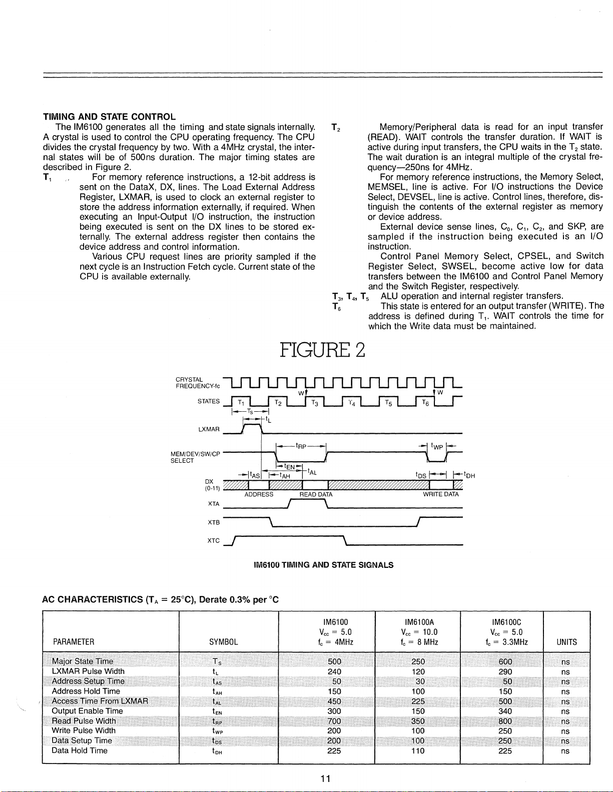
TIMING AND
STATE
CONTROL
The IM6100 generates all the timing and state signals internally.
A crystal
is
used to control the CPU operating frequency. The
CPU
divides the crystal frequency by two. With a 4MHz crystal, the internal states will
described
T1
be
in
of 500ns duration. The major timing states are
Figure
2.
For memory reference instructions, a 12-bit address is
on
sent
the DataX,
Register, LXMAR,
store the address information
executing
an
being executed is sent
DX,
lines. The Load External Address
is
used to clock
an
external register to
externally, if required. When
Input-Output I/O instruction, the instruction
on
the DX lines to
be
stored externally. The external address register then contains the
device address and
Various
next cycle
CPU
is
an
control information.
request lines are priority sampled
if
the
Instruction Fetch cycle. Current state of the
CPU is available externally.
T 2 Memory/Peripheral data
WAIT
(READ).
controls the transfer duration. If WAIT
active during input transfers, the
is
an
The wait duration
quency-250ns
for 4MHz.
integral multiple of the crystal fre-
For memory reference instructions, the Memory
MEMSEL, line
Select, DEVSEL, line
is active. For I/O instructions the Device
is
active. Control lines, therefore, distinguish the contents of the
or device address.
External device sense lines,
sampled if the
instruction
instruction.
Control Panel Memory Select, CPSEL, and Switch
Register Select, SWSEL, become active low for data
IM6100 and Control Panel Memory
and
internal register transfers.
T
Ts
transfers between the
and the
•
T
Ts
,
3
ALU
4
This state is entered for
address
Switch Register, respectively.
operation
is
defined during T1. WAIT controls the time for
which the Write data must
is
read for
CPU
external register
Co,
an
input transfer
waits
in
the
C1, C2, and
T2
as
memory
SKP,
being executed is an I/O
an
output transfer (WRITE). The
be
maintained.
is
state.
Select,
are
CRYSTAL
FREQUENCY·!e
STATES
LXMAR
MEMIDEVISWICP
SELECT
XTB
XTC
---+--.J
-1
IM6100 TIMING AND
AC CHARACTERISTICS (T A = 25°C), Derate 0.3% per
PARAMETER
SYMBOL
FIGURE
2
\~------------------~I
\~-----------------
STATE
SIGNALS
°C
IM6100
Vee = 5.0
fe = 4MHz
IM6100A
Vee = 10.0
fe
= 8
MHz
IM6100C
Vee = 5.0
fe = 3.3MHz
UNITS
MajorStqteTime
LXMAR Pulse Width
·Addre~s$etupTi.f11e
Address Hold Time
r\GcessTimeFromLXMAR
Output Enable
Pulse Width
Read
Write
Pulse Width
Data Setup Time
Hold Time
Data
Time·
tDH
500
240
50
150
450
300
700
200
200
225
11
Page 13
MEMORY
AND
PROCESSOR
INSTRUCTIONS
The
IM6100 makes no distinction between instructions
IM6100
manipulate instructions
instructions when it
classes
Reference
Output
Transfer Instruction (lOT).
Before proceeding further,
instructions are 12-bit words stored in memory. The
and
as
is
stored variables or execute data
programmed to do
so.
There are three general
of IM6100 instructions. They are referred to
data; it can
as
Memory
Instruction (MRI), Operate Instruction (OPR) and Input!
we
will discuss the Specific Memory
as
Organization with which thelM6100 interfaces.
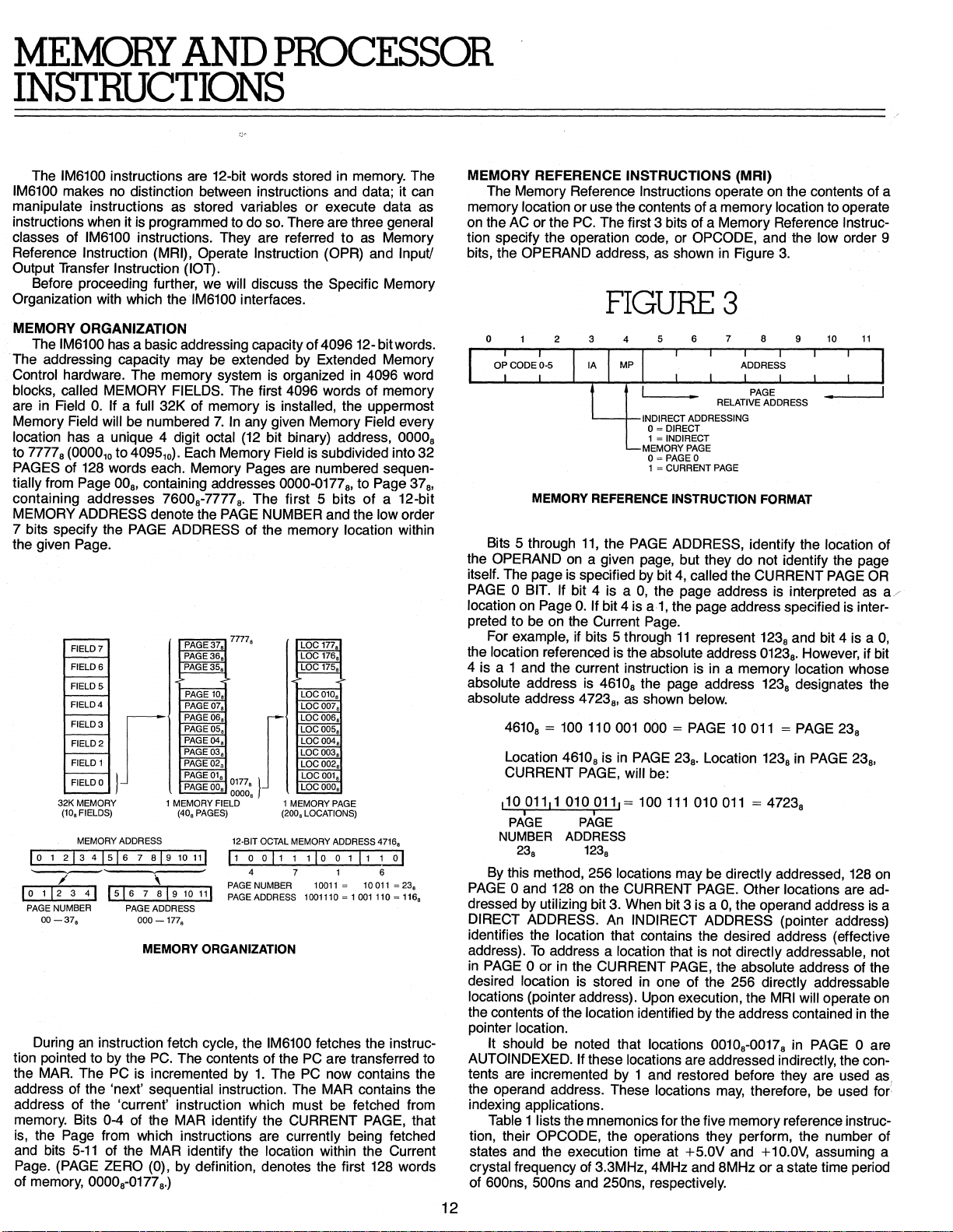
MEMORY ORGANIZATION
The IM6100
The addressing capacity may
Control hardware. The memory system
has
a basic addressing capacity of 409612-bit words.
be
extended by Extended Memory
is
organized
in
4096 word
blocks, called MEMORY FIELDS. The first 4096 words of memory
are
in
Field
O.
If a full 32K of memory
Memory Field will
be
numbered
7.
location has a unique 4 digit octal
to
77778
(000010
PAGES of
tially from Page
containing addresses
to 4095
128
words each. Memory Pages are numbered sequen-
OOe,
).
Each Memory Field
10
containing addresses
7600e-7777e. The first 5 bits of a 12-bit
is
installed, the uppermost
In
any given Memory Field every
(12
bit binary) address, 0000
is
subdivided into 32
0000-0177a,
to Page 37e,
MEMORY ADDRESS denote the PAGE NUMBER and the low order
7 bits specify the
PAGE
ADDRESS of the memory location within
the given Page.
7777,
PAGE
FIELD
7
FIELD 6
FIELDS.
4
FIELD
3
FIELD
FIELD 2
1
FIELD
FIELD 0
32K MEMORY
(10,FIELDS)
MEMORY ADDRESS
I 0 1 2 I 3 4
1516 7 819
~
10 1 12 3 41
PAGE
NUMBER
00
-37,
During
tion pointed to
the
MAR.
1516 7 819
PAGE
an
instruction fetch cycle, the
by
the
The PC is incremented
address of the 'next'
\
ADDRESS
000-177,
MEMORY ORGANIZATION
PC.
sequential instruction. The MAR contains the
37,
PAGE
36,
PAGE
35,
PAGE
10,
PAGE
07,
PAGE
06,
PAGE
OS,
PAGE
04,
PAGE
03,
PAGE
02,
PAGE
01,
PAGE
00,
1 MEMORY FIELD 1 MEMORY
(40,
10
~~~~:
PAGES)
12-BIT
111
1100111
4 7 1 6
PAGE
10
111
PAGE
NUMBER 1
ADDRESS 1001110 ~ 1 001110 ~ 116,
The contents of the
by
address of the 'current' instruction which must
memory. Bits
is,
the Page from which instructions are currently being fetched
and
bits
Page.
(PAGE ZERO (0), by definition, denotes the first
of memory,
0-4
of
the MAR identify' the CURRENT PAGE, that
5-11
of the MAR identify the location within the Current
OOOOe-Ol77
e.)
LOC
LOC
LOC
LOC010,
LOC007,
LOC006,
LOC
LOC
f
LOC
LOC002,
I
~gg
(200,
LOCATIONS)
OCTAL
MEMORY ADDRESS 4716,
do
IM6100
1.
fetches the instruc-
PC
The
PC
177,
176,
175,
005,
004,
003,
~~~:
PAGE
0111
1:=£]
0011 ~ 10011 ~ 23,
are transferred to
now contains the
be
fetched from
128
words
MEMORY REFERENCE INSTRUCTIONS (MRI)
The Memory Reference Instructions operate
memory
on
location or use the contents of a memory location to operate
the AC or the
PC.
The first 3 bits of a Memory Reference Instruction specify the operation code,
bits, the
OPERAND address,as shown
FIGURE
o 2
8
MEMORY REFERENCE INSTRUCTION FORMAT
Bits 5 through
the OPERAND
itself. The page
PAGE
0 BIT. If bit 4 is a
location
on
Page
preted to be on the Current
For example, if bits 5 through
the location referenced
4 is a 1 and the current instruction
absolute address
absolute address 4723e,
4610
e
Location
CURRENT
11001111
i ,
PAGE PAGE
NUMBER
23
8
By this method, 256 locations may
PAGE
0 and
dressed by utilizing bit 3. When bit 3 is a
DIRECT ADDRESS.
3
4
L--t-INDIRECT
11,
the PAGE ADDRESS, identify the location of
on
a given page, but they do not identify the page
is
specified
O.
If bit 4 is
is
the absolute address
is
4610e the page address
as
=
100
110
001
4610e is
010011
ADDRESS
128
in
PAGE,
will be:
= 100111 010011 = 4723
1
123
8
on
the CURRENT
An
INDIRECT ADDRESS (pointer address)
or
OPCODE,
in
5
6
ADDRESSING
o
~
DIRECT
1 = INDIRECT
MEMORY PAGE
0=
PAGE 0
1 = CURRENT PAGE
by
bit
4,
called the CURRENT
0,
the page address is interpreted
al,
the page address specified
Page.
11
represent 123e and bit 4 is a
is
in
shown below.
000 = PAGE
PAGE
23e. Location 123e in
be
PAGE.
on
the contents of a
and
Figure
the low order 9
3.
3
7
8
9
.
0123
However, if bit
a memory location whose
10
directly addressed,
0,
the operand address
8
designates the
123
e
011 = PAGE
e
Other locations
identifies the location that contains the desired address (effective
address).
in
desired
locations (pointer address). Upon execution, the
the contents of the location identified
PAGE
To
address a location that
0 or
in
location
the CURRENT
is
stored in one of the 256 directly addressable
is
not directly addressable, not
PAGE,
the absolute address of the
MRI
by
the address contained
will operate
pointer location.
It should
be noted that locations
0010
-0017
e
in
e
AUTOINDEXED. If these locations are addressed indirectly, the contents are incremented
the operand address. These locations
by
1 and restored before they are used
may,
therefore,
indexing applications.
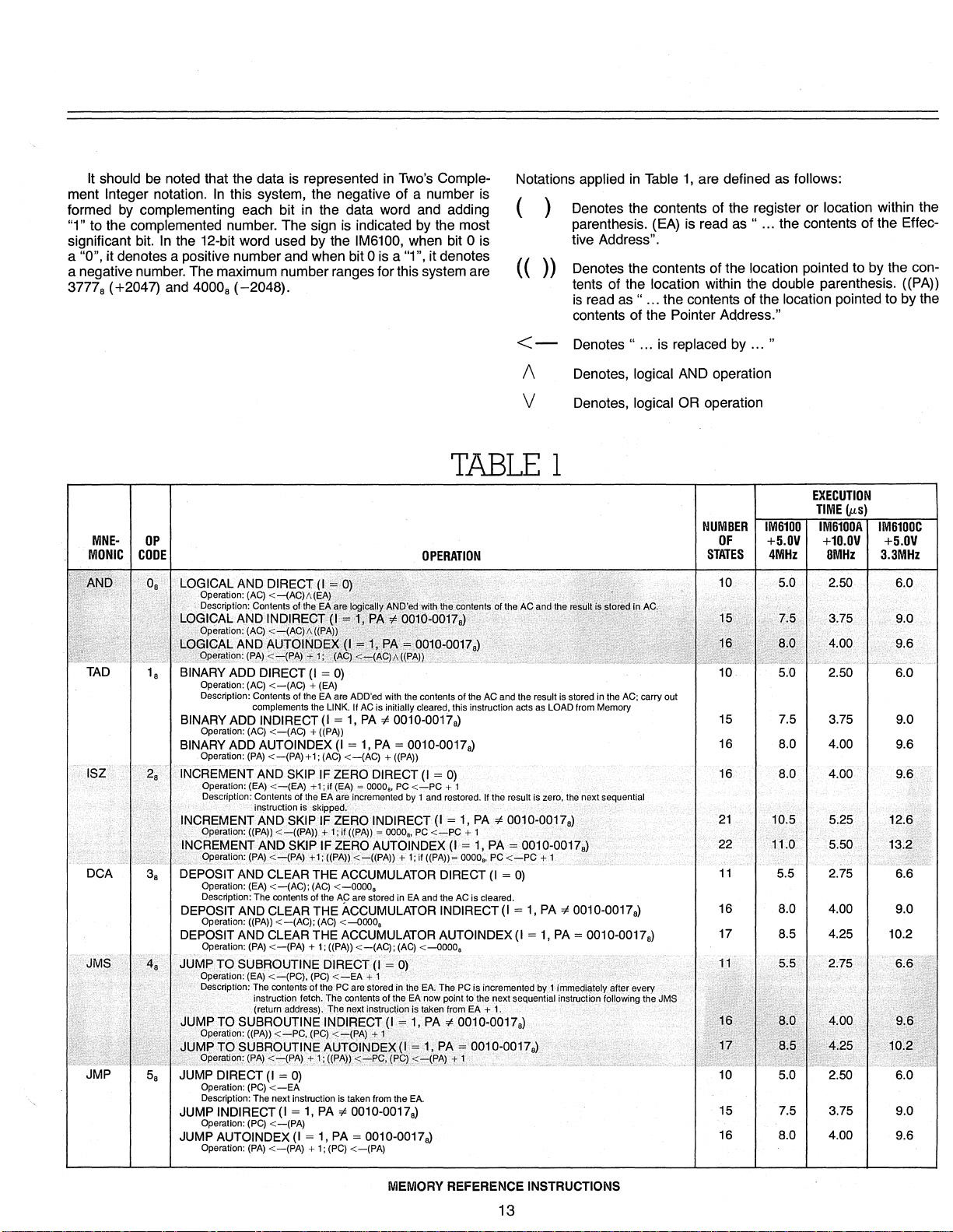
Table
tion, their
states
1 lists the mnemonics for the five memory reference instruc-
OPCODE, the operations they perform, the number of
and
the execution time at +5.0V and +10.0V, assuming a
crystal frequency of 3.3MHz, 4MHz and 8MHz or a state time period
of
600ns, 500ns
and
250ns, respectively.
12
10
PAGE
PAGE
PAGE
be
11
OR
as
is
inter-
0,
23
e
23e,
128
on
are
ad-
is
on
in
the
0 are
as.
used for
a -
a
Page 14
It
should be noted that the data is represented
ment Integer notation.
In
this system, the negative of a number is
in
Two's Comple-
formed by complementing each bit in the data word and adding
"1" to the complemented number. The sign is indicated by the most
In
significant bit.
a
"0", it denotes a positive number and when bit 0 is a "1", it denotes
the 12-bit word used by the IM6100, when bit 0 is
a negative number. The maximum number ranges for this system are
37778 (+2047) and
40008 (-2048).
Notations applied
( )
Denotes the contents of the register or location within the
parenthesis. (EA) is read as
in
Table
1,
are defined as follows:
" ... the contents of the Effec-
tive Address".
« »
Denotes the contents of the location pointed to by the contents of the location within the double parenthesis.
is
read as " ... the contents of the location pointed to by the
contents of the Pointer
Aqdress."
< - Denotes" ... is replaced by ... "
«PA»
DCA
TABLE
BINARY ADD DIRECT (I =
Operation: (AC)
Description: Contents of the EA are ADD'ed with the contents of the AC
BINARY ADD INDIRECT (I =
Operation:
BINARY ADD AUTOINDEX (I = 1, PA = 0010-0017a)
Operation:
~TI·T'7.""C··:':
..•..
<-(AC)
complements the
(AC)
<-(AC)
(PA)
<-(PA)+I;
....
.•
'mSl[ruClI:on
+<1'N·*J;«I?~\j)l::::..f~(PA))·
3a DEPOSIT AND CLEAR THE ACCUMULATOR DIRECT (I =
Operation:
Description: The contents of the
DEPOSIT AND CLEAR
Operation: ((PA))
DEPOSIT AND CLEAR THE ACCUMULATOR AUTOINDEX (I =
Operation:
(EA)
<-(AC);
(PA)
<-(PAl + 1;
<-(AC);
0)
+ (EA)
LINK.
If
AC
is initially cleared, this instruction acts
1,
+ ((PA))
SKIP IFZERODII::U:CT (I =
IS,:sKlppeQ.:':T:,
(AC)
THE
PA"# 0010-0017.)
(AC)
<-(AC)
+ «PA))
0)
. 0000" PC
'e)n.crennentec
~OINCHRI:Cl"(,
'-"".=
.-'~';';;;"''''''
<-0000,
AC
are stored in
ACCUMULATOR INDIRECT (I = 1, PA
(AC)
<-0000,
<-,-PC
+ 1 .
by
1 and restored. If the result is zero,
uuuu.
.1= 1, PA4.001Q-OQ17a)'{
PC'~
" .
(1:= 1
«PA))", 0000"
and the
AC
<-0000,
,+ ~ ';,
NDEX
',1
;if
EA
.•
,PA='cib10~001T
PC<-:--:!,~
is cleared.
1\
Denotes, logical AND operation
V Denotes, logical OR operation
1
and
the result
is
stored in the AC; carry out
as
LOAD from Memory
. .
,,"'"
'
the
next sequential
','
'~;T:~,';T'
:T',T
,""
,',
,:"i:,~;'{:0,~!,:,,:)'
t!'.;:i:'.i;;u.';'
0)
1,
PA
,'(~'"
,;(:'
40010-0017
= 0010-0017
)
a
a)
10
15
16
1,6
11
16
17
5.0
7.5
8.0
5.5
8.0
8.5
2.50
3.75
4.00
2.75
4.00
4.25
IM6100C
+5.0V
3.3MHz
6.0
9.0
9.6
6.6
9.0
10.2
JMP
5.
JUMP DIRECT (I =
Opemtion: (PC)
Description: The next instruction
JUMP INDIRECT (I =
Opemtion: (PC)
JUMP AUTOINDEX (I = 1, PA = 0010-0017
Opemtion:
<-EA
<-(PAl
(PA)
<-(PAl + 1;
0)
is
1,
PA
4 0010-0017.)
(PC)
taken
from
the
EA.
<-(PAl
a)
MEMORY REFERENCE INSTRUCTIONS
13
10
15
16
5.0
7.5
8.0
2.50
3.75
4.00
6.0
9.0
9.6
Page 15

OPERATE
INSTRUCTIONS
The Operate Instructions, which have
consists of 3 groups of microinstructions. Group 1 microinstructions,
which are identified
perform
link. Group 2 micro instructions, which are identified by the presence
of a 1
of the
instruction. Group 3 microinstructions have a 1
bit
the AC and
logical operations
in
bit 3 and a 0 in bit
accumulator and then conditionally skip the next sequential
11
and are used to perform logical operations
MO.
The basic OPR instruction format is shown
by
the presence of a 0 in bit
on
the contents of the accumulator and
11,
are used primarily to test the contents
an
OPCODE of
in
on
in
Figure 4.
78
(111),
3,
are used to
bit 3 and a 1 in
the contents
of
FIGURE
3 4
2
A
1
I
MICROINSTRUCTION
GROUP 1
GROUP 2
GROUP
BASIC OPR INSTRUCTION FORMAT
I
0
1
: 1 :
Operate microinstructions from any group may be microprogram-
med
with other operate microinstructions of the same group. The
actual code for a microprogrammed combination of two, or more,
logical
OR
microinstructions is the bitwise
individual microinstructions. When more than one operation
programmed into a
in
a prescribed sequence, with logical sequence number 1 microinstructions performed first,
tions performed second,
tions performed third and
logical sequence number, within a given group of microinstructions,
are performed
single instruction, the operations are performed
logical sequence number 2 microinstruc-
logical sequence number 3 microinstruc-
so
on.
simultaneously.
of the octal codes for the
Two
operations with the same
4
5
3 1 1
7 8 9 10
6
o -t
An
1
0
:
11
B I
is
micro-
i4
Page 16
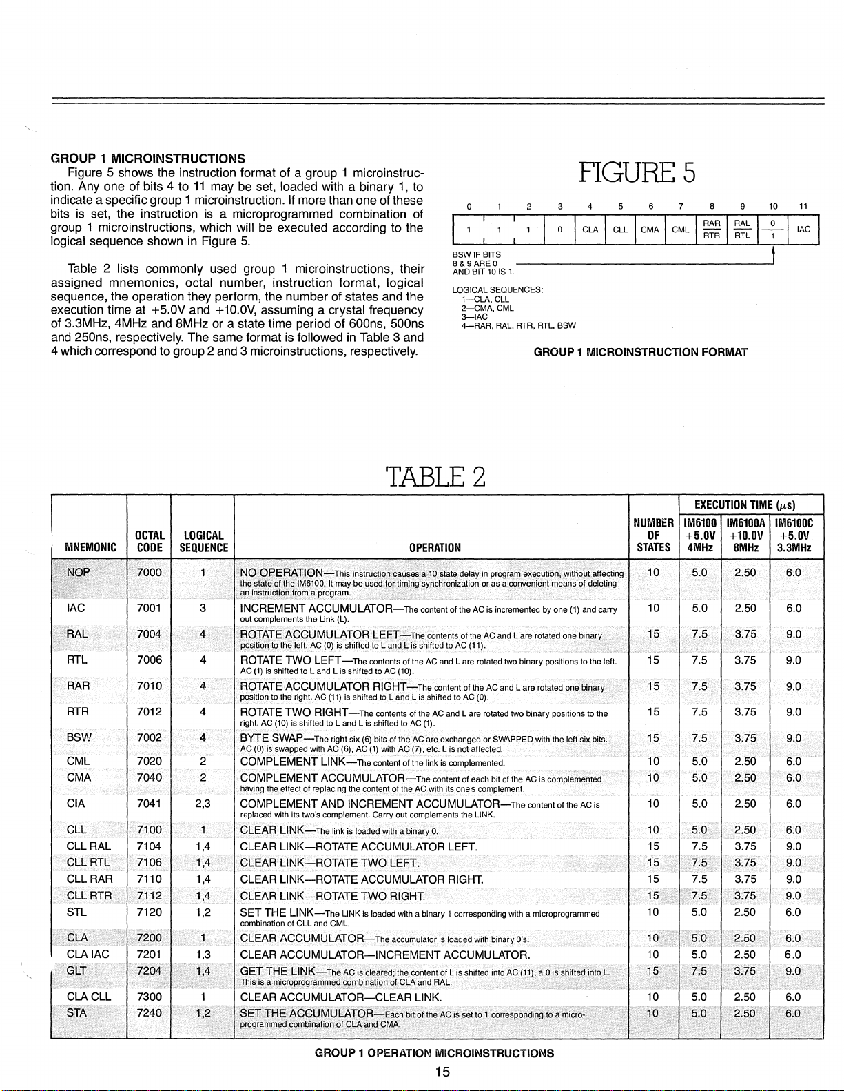
GROUP 1 MICROINSTRUCTIONS
Figure 5 shows the instruction format
tion.
Anyone
of bits 4 to
11
may be set, loaded with a binary
indicate a specific group 1 microinstruction.
bits
is
set, the instruction
is
a microprogrammed combination of
of
a group 1 microinstruc-
1,
If more than one of these
to
group 1 microinstructions, which will be executed according to the
logical sequence shown
in
Figure
5.
Table 2 lists commonly used group 1 microinstructions, their
assigned mnemonics, octal number, instruction format, logical
sequence, the operation they perform, the number of states and the
execution time at
of
3.3MHz, 4MHz and 8MHz or a state time period of 600ns, 500ns
and 250ns, respectively. The same format is followed
+5.0Vand
+10.0V, assuming a crystal frequency
in
Table 3 and
4 which correspond to group 2 and 3 microinstructions, respectively.
o 2
BSW
IF
BITS
8 & 9
ARE
AND
BIT
10
LOGICAL
SEQUENCES:
1-CLA.CLL
2-CMA.CML
3-IAC
4-RAR,
FIGURE
3 4
0
IS
1.
RAL,
RTR,
RTL,
BSW
GROUP 1 MICROINSTRUCTION FORMAT
5 6 7 8 9
5
10
11
RTR
SSW
CML
CMA
CIA
CLL
4
4
2
RPTjI,TE
I(osition.tothe left.
ROTATE
AC
ROTATE
position
ROTATE
right.
BYTE
AC
COMPLEMENT
COMPLEMENT
having
COMPLEMENT
replaced
CLEAR
CLEAR
CLEAR
CLEAR
CLEAR
SET
combination
CLEARAgCUMU
CLEAR
GET
This
ACCU
MU
LATOR
AC
(0)
is shifted
TWO
(1)
is
to
AC
SWAP-The
(0)
is
the
THE
TI-iE
i~a
LEFT
Shifted
to
Land L is shifted
ACCUMULATOR
the right.
AC
(11)
TWO
RIGHT-The
(to)
is
shifted
to
Land L is
swapped
effect of replacing the content
with
LINK-The
LINK-ROTATE
LINK-ROTATE
LINK-ROTATE
LINK-ROTATE
of
ACCUMULATOR-INCREMENT
rnicroprograrnmedcombirationofCLA
right six
with
AC
LINK-The
ACCUMULATOR-The
AND
its
two's
complement. Carry out complements the
link
LINK-The
CLL
and
CML.
LATOR-The
IJNl)--,TheACisclea,red;theconlent
LEF[
to
Land
-The
contents
to
RIGHT-The
is
shifted
to
contents
shifted
(6)
bits
(6),
AC
(1)
with
content
INCREMENT
is
loaded
ACCUMULATOR
TWO
ACCUMULATOR
TWO
LINK
is
loaded
TABLE
OPERATION
-The.
contents of the
L.is shifted
of
AC
(10).
Land L is shifted
to
of
the
AC (7),
of
of
the
with
abinary.O.
LEFT.
RIGHT.
with
accumulator
to
AC
the
AC
and L are
content
of
to
AC
of
the
AC
and L are
AC
(1).
AC
are exchanged
etc.
L is
not
the link
is
complemented.
content
AC
ACCUMULATOR-The
a binary 1 corresponding
and
of
with
its on9's complement.
LEFT.
RIGHT.
is
loaded
ACCUMULATOR.
of
L is shifted into AC(11),
RAL.
2
AC
and L are rotated one
(11).
rotated
two
binary positions to the left.
the
AC
and
L are rotated one binary
(0). .
rotated
two
binary positions
or
SWAPPED
affected.
each bit
LINK.
with
binary a's.
with the lett sixbits.
of
the
AC
is complemented
content
with
a microprogrammed
of
the ACis
NUMBER
OF
STATES
EXECUTION
IM6100
+5.0V
4MHz
TIME
IM6100A
+10.0V
BMHz
(MS)
IM6100C
+5.0V
3.3MHz
6.0
6.0
9.0
9.0
3.75
to
the
3.75 9.0
9,0
3.75 9.0
GROUP 1 OPERATION MICROINSTRUCTIONS
15
Page 17
OPERATE
GROUP 2 MICROINSTRUCTIONS
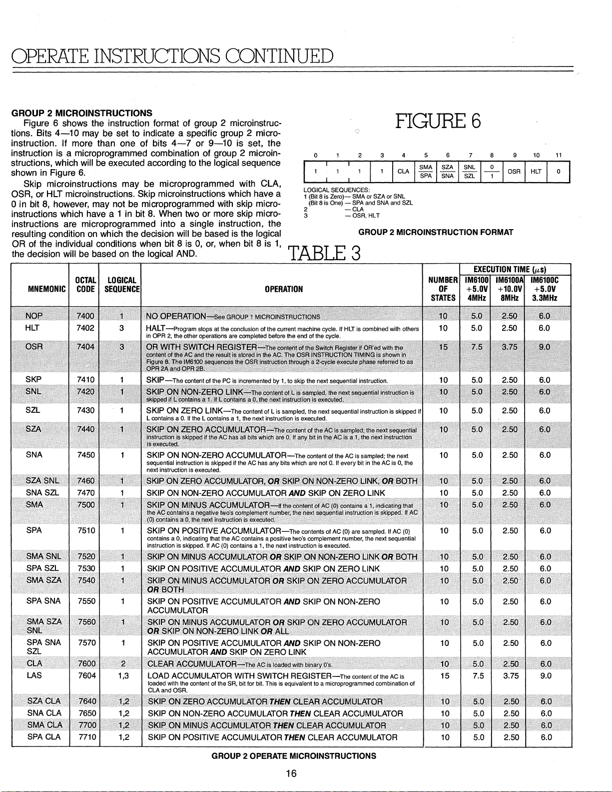
Figure 6 shows the instruction format of group 2 microinstructions. Bits
instruction.
instruction is a microprogrammed combination of group 2 microinstructions, which
shown in Figure
Skip microinstructions may be microprogrammed with CLA,
OSR, or HLT microinstructions. Skip microinstructions which have a
o in bit
instructions which have a 1 in bit
instructions are microprogrammed into a single instruction, the
resulting condition
OR
the decision will be based on the logical AND.
4-10
If more than one of bits
8,
however, may not be microprogrammed with skip micro-
of the individual conditions when bit 8 is
INSTRUCTIONS
may be set to indicate a specific group 2 micro-
4-7
will
be
executed according to the logical sequence
6.
8.
When two or more skip micro-
on
which the decision will be based is the logical
CONTINUED
or
9-10
is set, the
0,
or,
when bit 8 is
o 2 3 4 5 6 7 8 9 10
LOGICAL SEQUENCES:
1 (Bit 8 is
(Bit 8 is One) -
2
3
1,
TABLE
FIGURE
Zero)-
SMA
or
SZA or SNL
SPA
and SNA and SZL
-CLA
-OSR.
HLT
GROUP 2 MICROINSTRUCTION FORMAT
3
6
11
MNEMONIC
OCTAL
CODe
OPERATION
SPA CLA
7710 1,2
SKIP ON POSITIVE ACCUMULATOR
GROUP 2 OPERATE MICROINSTRUCTIONS
THEN
CLEAR ACCUMULATOR 10
16
5.0 2.50
6.0
Page 18

GROUP 3 MICROINSTRUCTIONS
Figure 7 shows the instruction format of group 3 microinstructions
which requires bits 3 and
set to indicate a specific group 3 microinstruction.
of the bits
is
set, the instruction is a microprogrammed combination
of group 3 microinstructions
Figure
7.
OCTAL
MNEMONIC
CODE
11
to contain a
1.
Bits 4, 5 or 7 may be
If more than one
following the logical sequence listed in
LOGICAL
SEQUENCE
0
1
I
LOGICAL
l-CLA
2-MOA.
3-ALL
TABLE
OPERATION
: 1 :
SE~UENCE:
MOL
OTHERS
4
FIGURE
2 3
1 I 1
GROUP 3 MICROINSTRUCTION FORMAT
4
CLA
5 6 7
>OAI
7
8 9
MO<
EXECUTION
NUMBER
STATES
OF
IM6100
+5.0V
4.0MHz
IM6100A
+10.0V
8.0MHz
TIME
10
*Oon't Care
(ILS)
IM6100C
+5.0V
3.3MHz
11
CLASWP
7721
NO
OPERATION-See
MQ
REGISTER
original content of the
MQ
REGISTER
tent
of
the
AC
content
SWAP
interchanged
CLEI)RI)CCtJMm.~1}c:5R
CLEAR
loaded
CLEARAccofVjULAfORANClL.OACl
TOR
3
CLEAR
REGISTER-The
MO
and the resu.ltis 10adedintotre.AC,
of
the.MOisr~t~in~(j;Ihis.in~tr~ctio!)Pr8vi~!,,,tl)eprog"lrlJlT)er
ACCUMULATOR
accomplishing a microprogrammed combination
ACCUMULATOR
with
binary
·.·.·Thi~i¢~ui~~le"tto.1).lT)i~rOh((Jgm~~~d·
ACCUMULATOR
is
loaded
into
the
Group
1 Microinstructions 10
LOAD-The
MQ
is lost.
INT9.A,.CCU~LJL}\"'9R-The
O's.
This
content
AC
and the
GROUP 3 OPERATE MICROINSTRUCTIONS
AND
is
equivalent
of
the
;
AND
AND
AC
MO
content
MQ
MQ
to
SWAP
is
is
cleared.
FIGURE
,
LXMAR
lfl
MEMSEL~~--~::::::j::::::::::::::t::::::::::::j
I
SWSEL:
I
DX I
®
~%~~W~~~~~~~~~~
CD
® ®
CD
Instruction
®
Address
Instruction ~ CPU
of
the
AC
is
loaded
into
contentCl(lheMO.isOR·ed
T.he
Origin~1
cont~nt
REGISTER-The
REGISTER-The
a microprogrammed
MOREGiSTER
D8mbin~tiOn
ACCUMULATOR
cleared. The content
of
MOA
combinalion
of.Gli\~n~MgA:'j
of
the
8
®
Switch
Register. ~ CPU
the
MO,
the
AC
is
cleared and the 10
with
AC
and
AC
and
MQ
OPR2B
the con-
the original
operation.
MO
and
MO
MOL.
are
are
of
\h~!lGislostbyt
withar.incl~sive.()R
content
of
the
and
MOL.
content
of
the
of
CLA
INfbACdJfVjOCA-'
AND
:
L.J
~~~
Data
10
5.0 2.50 6.0
5.0 2.50 6.0
5.0 2.50 6.0
5.0
5.0
2.50
6.0
2.50 6.0
5.0 2.50 6.0
5.0 2.50
6.0
5.0 2.50 6.0
OSR INSTRUCTION TIMING
17
Page 19
INPUT/OUTPUT
TRANSFER
INSTRUCTIONS
The input/output transfer instructions, which have
6
,
are used to initiate the operation of peripheral devices and to
a
transfer data between peripherals and the
data transfer may be used to receive or transmit information between
IM6100 and one or more peripheral I/O devices. PROGRAMMED
the
DATA
TRANSFER provides a straightforward means of communicating with relatively slow
card readers and CRT displays.
interrupt system to service several peripheral devices simultaneously, on
to be performed concurrently with the data
grammed Data Transfers and Program
accumulator as a buffer, or storage area, for
data may be transferred only between the accumulator and the
peripheral, only one
DIRECT MEMORY ACCESS, DMA, transfers variable-size blocks of
data between high-speed peripherals and the memory with a minimum of program control required by the
lOT INSTRUCTION FORMAT
and the execution time at
frequency of 3.3MHz, 4MHz and 8MHz or a state time period of
600ns, 500ns and 250ns, respectively is represented
an
intermittent basis, permitting computational operations
Input/Output Transfer Instruction format, the number of states
The
I/O devices, such
INTERRUPT TRANSFERS use the
12
bit word at a time may be transferred.
+5.0V
and +10.0V, assuming a crystal
(lOT)
an
OPCODE of
IM6100. Three types of
as
Teletypes, cassettes,
I/O operations. Both Pro-
Interrupt Transfers use the
a"
data transfers. Since
IM6100.
in
Figure
9.
approach. The data transfer begins when the IM6100 fetches
instruction from the memory and recognizes that the current instruc-
lOT.
This
is
tion is an
internal states. The
2-cycle execute phase referred to as
lOT instruction are available
must be latched in an external address register.
low to enable data transfers between the IM6100 and the peripheral
device(s).
The selected peripheral device communicates with the IM6100
through 4 control
of data transfer, during
eral device(s) by asserting the control lines
The control line
to skip the next sequential instruction. This feature
the status of various signals
C
lines are treated independently of the SKP line.
2
RELATIVE or ABSOLUTE JUMP, the skip operation
after the jump. The input signals to the
and
the
cycle is internal to the IM6100 to perform the operations requested
during
Input-Output Instruction Timing
SKP,
are sampled at
IM6100 is available to the device(s) during
IOTA'
Both
referred to as IFETCH and consists of five (5)
IM6100 sequences the lOT instruction through a
IOTA
lines-Co,
an
SKP,
when low during
IOTA
and
on
DX
0-11
C"
C2 and
lOT instruction, is specified by the periph-
in
the device interface. The
IOTA
during DEVSEL· XTc. The data from
lOTs
consist of six
and lOTs. Bits
at
IOTA' LXMAR. These bits
is
shown
SKP.
In the IM6100 the type
as
shown in Table
an
lOT,
causes the IM6100
IM6100, DX
DEVSEL·XT
(6)
0-11
DEVSEL is active
in
Figure
is
used to sense
Co,
In
the case of a
is
performed
0-11,
Co,
internal states.
of the
C"
C"
.
c
an
10.
5.
and
C
lOTs
,
2
The first three bits, 0-2, are always set to 6a (110)
lOT instruction. The next six bits, 3-8, contain the device selection
code that determines the specific
struction is intended and, therefore, permit interface with up to
devices. The last three bits,
code that determines the specific operation to be performed. The
nature of this operation for any given
tirely upon the circuitry designed into the
PROGRAMMED DATA TRANSFER
Programmed Data Transfer is the easiest, simplest, most convenient and most common means of performing data
processor applications, it may also be the most cost effective
FIGURE
o 2 3
4 5 6 7
lOT INSTRUCTION FORMAT
I/O device for which the lOT in-
9-11,
contain the operation specification
lOT instruction depends en-
I/O device interface.
9
to specify an
I/O. For micro-
9
8
10
64
I/O
11
TABLE
CONTROL
Co
C,
LINES
C
2
OPERATION
In
summary, Programmed Data Transfer performs data I/O with a
minimum of hardware support. The maximum rate at which program-
+5.DV
3.3MHz
10.2
IM6100 instruc-
IM6100. The
On
the
a"
med data transfers may take place is limited by the
tion execution rate. However, the data rate of the most commonly
used peripheral devices is much lower than the maximum rate at
which programmed transfers can take place in the
major drawback associated with Programmed Data Transfer is that
IM6100 must hang
the
pletes the last transfer and prepares for the next transfer.
other hand, this technique permits easy hardware implementation
and simple, economical interface design. For this reason, almost
devices except bulk storage units rely heavily on programmed data
transfer for routine data
lOT NUMBER
up
NUMBER
OF
STATES
17
in a waiting loop while the I/O device com-
I/O.
EXECUTION
TIME
(ILS
IM6100
+5.0V
4MHz
OF
IM6100A
+10.0V
8MHz
8.5
4.25
STATES/EXECUTION TIME
IM6100C
5
DESCRIPTION
'Don't
Care
L L
PC
<-DEV
:t~~;6oote~{0ftn~~Cis.
The content of the AC is sent to a device and then the AC is cleared.
i
tq~tli'i~
~ei~ly~gfr()rn
s'etlt,
tothed~vi~.i
a~~SiG~;;gFi:~d'Wjih~hie'g~t~
irrth~f.<::ar(j
theresuitiisstor,i(fioih~,A.C.
REl:A'-i~E;.JUM,B··
Data is received from a device and loaded into the PC. This is referred to as an ABSOLUTE JUMP.
PROGRAMMED
I/O CONTROL LINES
18
i
Page 20
FIGURE
10
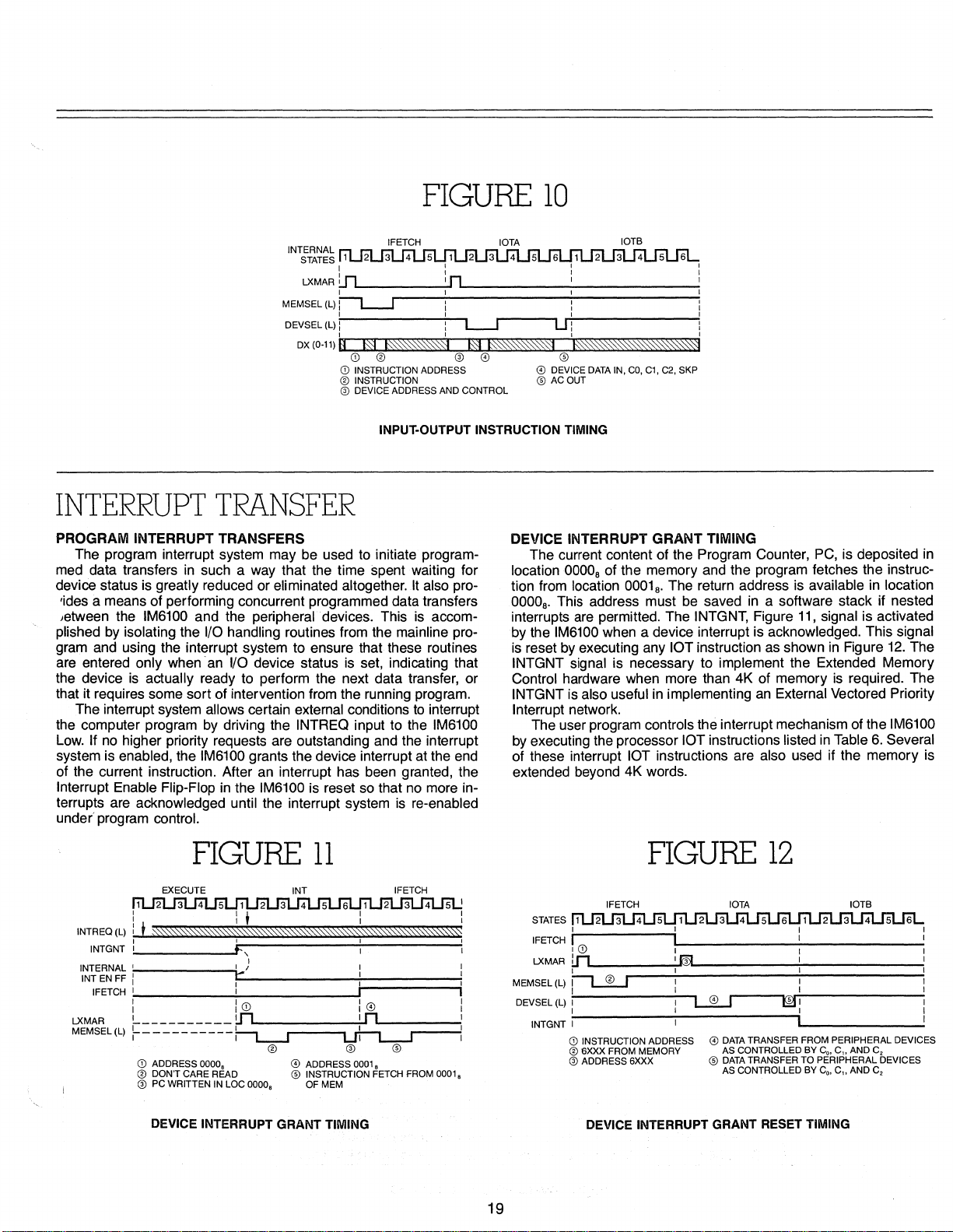
IFETCH
1
________
~:n
~----------~--------------~
L-1
t§l
~~~~~
o ® @ @ ®
INPUT-OUTPUT INSTRUCTION TIMING
~
INTERRUPT
TRANSFER
INTERNAL
STATES
, I
~MARUl,--
MEMSEL (L)
DEVSEL (L) : :
1 -
~.-------:----------------+:----------------i
1
DX(0.11)H
o INSTRUCTION ADDRESS @ DEVICE
® INSTRUCTION ® AC OUT
@ DEVICE ADDRESS AND CONTROL
PROGRAM INTERRUPT TRANSFERS
The program interrupt system may be used to initiate program-
in
med data transfers
device status is greatly reduced or eliminated altogether.
such a way that the time spent waiting for
It
also pro'ides a means of performing concurrent programmed data transfers
,etween the
IM6100 and the peripheral devices. This is accomplished by isolating the I/O handling routines from the mainline program and using the interrupt system to ensure that these routines
are entered only when
is
the device
actually ready to perform the next data transfer, or
an
I/O device status is set, indicating that
that it requires some sort of intervention from the running program.
The interrupt system
the computer program
Low.
If
no
higher priority requests are outstanding and the interrupt
system is enabled, the
allows certain external conditions
by
driving the INTREQ input to the IM6100
to
interrupt
IM6100 grants the device interrupt at the end
of the current instruction. After an interrupt has been granted, the
Interrupt Enable Flip-Flop
terrupts are acknowledged until the interrupt system
in
the IM6100 is reset so that no more in-
is
re-enabled
under program control.
IOTA
~'----------------i
U :
&~~~~
'~~~~",~~\~~\~
DATA
IN,
CO,
C1,
C2, SKP
DEVICE INTERRUPT GRANT TIMING
The current content of the Program Counter,
location
tion from location
0000
interrupts
by the
is reset by executing any
00008 of the memory and the program fetches the instruc-
,
0001
The return address is available in location
,
This address must be saved
8
are
permitted. The INTGNT, Figure
8
in
a software stack if nested
IM6100 when a device interrupt is acknowledged. This signal
lOT instruction as shown
PC,
is deposited in
11,
signal is activated
in
Figure
INTGNT signal is necessary to implement the Extended Memory
is
Control hardware when more than 4K of memory
INTGNT is also useful in implementing
an
External Vectored Priority
required. The
Interrupt network.
The user program controls the interrupt mechanism of the
by
executing the processor lOT instructions listed
of these interrupt
lOT instructions are also used if the memory is
in
Table
6.
extended beyond 4K words.
12.
The
IM6100
Several
FIGURE
EXECUTE
INT
EN
FF : 1
IFETCH , I
INTERNAL
t=====J=======J======~
~
o ADDRESS 0000,
® DON'T CARE READ
@ PC WRITTEN IN LOC 0000,
DEVICE INTERRUPT GRANT TIMING
11
INT
________
®
@ ADDRESS 0001,
® INSTRUCTION FETCH FROM 0001,
OFMEM
:@
~:n~
__
I
@ ®
IFETCH
~==~
19
STATES
IFETCH I
~MAR
MEMSEL(L)
DEVSEL (L)
INTGNT I
FIGURE
IFETCH
1
1
10
lI1'--
________
1
~
I I
!..,
-----------:.---.~r----...,@r.,---------------:
, 1
o INSTRUCTION ADDRESS @
® 6XXX FROM MEMORY AS CONTROLLED BY
@ ADDRESS 6XXX ®
DEVICE INTERRUPT GRANT RESET TIMING
~
L----------.;.-----------i
12
IOTA
,
IL.
____________
DATA
TRANSFER FROM PERIPHERAL DEVICES
DATA
TRANSFER TO PERIPHERAL DEVICES
AS CONTROLLED
BY
Co,
Co,
C"
C"
AND
AND
C,
C,
---..:
Page 21
INPUT/OUTPUT
TRANSFER
INSTRUCTIONS
CONTINUED
TABLE
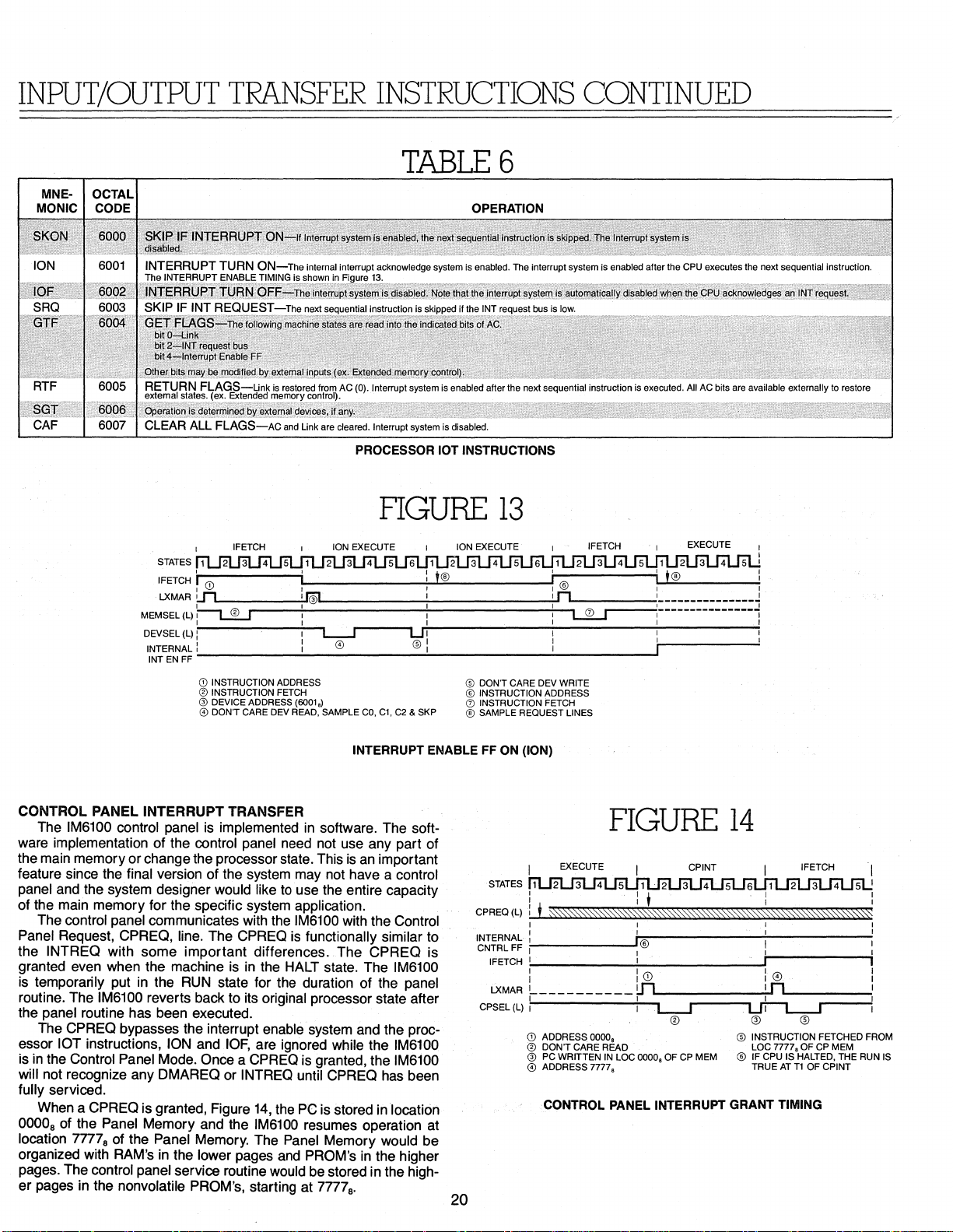
PROCESSOR lOT INSTRUCTIONS
FIGURE
STATES
IFETCH
~MARur1~;_;:::::f:~~®~::::::::::::±:::::::::::::~~~;_;:::~'
MEMSEL
(L)
DEVSEL
(L)
INTERNAL i : ® ® i
INTENFF~-----~-------~------~-----~
IFETCH
1 1 2
r!
(iQ);------jiL
~:
I I I I I
i I
ION
EXECUTE
______
L-'
..J...~
______
I
U I :
ION
6
13
EXECUTE
IFETCH
J_;;;_-----L,
LS2.....J
EXECUTE
.tt®~8~
___
::::::::::::::::~
1-1
-----....:
~,
I
CD
INSTRUCTION
® INSTRUCTION
®
DEVICE
® DONT
ADDRESS
CARE
DEV
ADDRESS
FETCH
(6001,)
READ,
SAMPLE
CO,
C1,
C2 & SKP
INTERRUPT ENABLE FF ON (ION)
CONTROL PANEL INTERRUPT TRANSFER
The IM6100 control panel is implemented in software. The software implementation
the main memory
of
the control panel need not use any part of
or
change the processor state. This
is
an
important
feature since the final version of the system may not have a control
panel and
system designer would like
to
use the entire capacity
the
of the main memory for the specific system application.
The control panel communicates with the
Panel Request, CPREQ,
the
INTREQ with some
line, The CPREQ is functionally similar to
important
granted even when the machine is in the HALT state, The
IM6100 with the Control
differences.
The
CPREQ is
IM6100
is temporarily put in the RUN state for the duration of the panel
routine. The
IM6100 reverts back to its original processor state after
the panel routine has been executed.
The CPREQ bypasses the interrupt enable system and the proc-
essor lOT instructions, ION and
IOF,
are ignored while the IM6100
is in the Control Panel Mode. Once a CPREQ is granted, the IM6100
will
not recognize any DMAREQ or INTREQ until CPREQ has been
fully serviced.
14,
When a CPREQ is granted, Figure
OOOOa
of the Panel Memory and the IM6100 resumes operation at
location
7n7
a of the Panel Memory. The Panel Memory would be
the PC is stored in location
organized with RAM's in the lower pages and PROM's in the higher
pages. The control panel service routine would be stored in the
er pages in the nonvolatile PROM's, starting at
7n7
.
a
high-
® DONT
CARE
DEV
®
INSTRUCTION
® INSTRUCTION
®
SAMPLE
STATES
CPREQ(L)
INTERNAL :
CNTRL
FF
IFETCH
~MAR
CPSEL (L) I I .
WRITE
ADDRESS
FETCH
REQUEST
LINES
EXECUTE
W-~~~~~~~~~~~~~~~~~~~~
--------hI®5""""------II------~
;-
~-----+'
~1~~::::~~~1l~-~::::::~~:r1~-~::::~
CD
ADDRESS 0000,
® DONT CARE
®
PC
WRITTEN
o ADDRESS 7777,
CONTROL PANEL INTERRUPT
20
FIGURE
I
I
I I
------....:...~I------l
I Q) : 0
L.....J
CPINT
14
.
ur-L....J
IFETCH
® ® ®
READ
IN
LOC
0000,
OF
CP
® INSTRUCTION FETCHED
LOC 7777,
® IF
MEM
CPU
TRUE
GRANT
OF
IS
HALTED,
AT
T1
OF
TIMING
CP
MEM
THE
CPINT
FROM
RUN
IS
Page 22
A Control Panel Flip-Flop,
IM6100,
further
Select,
is set when the CPREO is granted. The
CPREO's from being granted.
As long as the
CPSEl,
CNTRl
is active instead of the Memory Select, MEMSEl, for
memory references. The
CNTRl
FF,
which
is
CNTRl
FF
is set, the Control Panel Memory
CPSEl
signal
may,
therefore,
internal
FF prevents
be
used
to
the
distinguish the Control Panel Memory from the Main Memory. How-
ever, during the Execute phase of indirectly addressed AND,
ISZ
or DCA instructions, the
MEMSEl
is made active. The instruc-
TAD,
tions are always fetched from the control panel memory. The oper-
and
address for indirectly addressed AND,
first to the control panel memory for
turn, refers
tion
dressed
cation
to
a location
may,
therefore, be examined and changed by indirectly ad-
TAD
and DCA instructions, Figure
in
the main memory is accessible to the control panel routine.
in
the main memory. A main memory loca-
FIGURE
INDIRECT
_____
I@
I~rl~
____
L--l
CP
MEMORY
STATES
IFETCH
~MAR
CPSEL(L)
MEMSEL
DATAF
IFETCH
1
I
1,--------,1-
I I I
I~
Ul~
_____
I I I 1
~
I ® 0 I I
I I I
(L)
I '----J LJi
I ®
I I
;",,1
____________
(7)
INSTRUCTION ADDRESS
® INSTRUCTION
@ EFFECTIVE ADDRESS
o OPERAND ADDRESS
FROM
CP
MEMORY
FROM
....
TAD,
an
effective address, which,
ISZ or DCA refers
15,
respectively. Every
15
DCA
EXECUTE
--,-
________
I®
~Ir1~
______
-----'I--------I
--'
® OPERAND ADDRESS
® DON'T
CARE
MAIN
(7)
AC WRITTEN INTO
MEM
MAIN
(7)
READ
MEMORY
~
I
Exiting
from
the control panel routine
following sequence with reference made to Figure
is
achieved by executing the
16.
ION
OOOOa
(loc
OOOOa
in
JMP I
The
ION,
6001
instruction will reset the CP FF after executing
,
the next sequential instruction. The
to
system since the
a
CNTRl
FF
is
still active. location
CPMEM)
ION
will not affect the interrupt
CPMEM contains either the original return address deposited
IM6100 when the
address defined by
lOAD
ADDRESS SWITCH. CPREO's are normally generated
in
manual actuation of the control switches.
be displayed
CP
routine was entered, or it may be a new starting
the
CP
routine, for example, by activating the
If the CPU registers must
in
real-time, the CPREO's must be generated by a timer
at fixed intervals.
lo-
The designer may also make use of the control panel features to
in
the
CP
implement Bootstrap loaders
Memory
so
will be "transparent" to the main memory. Programs will be loaded
by DCA
CP
I POINTER instruction, the pointer being developed
RAM
to
point to the main memory location to be loaded.
64
Approximately
P/ROM locations are sufficient to implement all
the functions of the PDP8/E Control Panel. The IM6100 provides for
a
12
bit switch register which can be read by the
program control with the
struction even without a control panel.
.
An
RTF,
6005
a
Exiting from a panel routine can
OR
THE SWITCH REGISTER, OSR, in-
instruction also resets the internal
,
be
achieved by activating the RE-
SET line since RESET has a higher priority than CPREO as shown
Figure 18. If the RUN/HlT line is pulsed while the IM6100 is
panel mode, it will 'remember' the pulse(s) but defer any action until
IM6100
the
I
exits from the panel mode.
OOOOa
of the
by
the
by
the
that the loader
in
the
IM6100
under
CNTRl
FF.
in
in
the
"DCA
INDIRECT" IN CONTROL PANEL ROUTINE
FIGURE
ION
STATES
1
EXECUTE
5
IFETcHr'~~~~----L-------~-----------f'7.®~---------Li----------~L-
~MARLI1~;_;:::::~~::::::::::::~::::::::::::~I:r1~~;_;:::::j:~~~~~~::::+=::::::::::~
CPSEL
(L)
~
DEVSEL (L):-:
INTERNAL: 0 ® i :
CNTRLFF~----------~--------------~--------------~----------~----------_;
1 1
-------------:--...,L-Jr-----,W..:-I----------------:--------------:-------------i--------------:
~ INSTRUCTION
® INSTRUCTION
@ DEVICE ADDRESS
o DON'T CARE DEVICE
® DON'T CARE
ADDRESS
FETCH
(6001,)
DEVICE
FROM
READ.
WRITE
CP
MEM
SAMPLE
CO.
C1.
"ION; JMP I 0000
:
C2 & SKP
ION
EXECUTE
2
® INSTRUCTION ADDRESS
(7)
INSTRUCTION
® EFFECTIVE
®
JMP
®
IF
IN
CONTROL PANEL ROUTINE
"
8
ADDRESS
CPU
WAS
16
L2...J
FETCH
ADDRESS
FROM
IN
THE
IFETCH
FROM
(0000,)
CP
HALT
CP
MEM
STATE.
I LJ2...j
MEM
LOC
0000,
THE
RUN
INDIRECT
IS
FLASE
____________
AT
T1
EXECUTE
JMP
__________
~
I
~®
21
Page 23
INPUT/OUTPUT
TRANSFER
INSTRUCTIONS
CONTINUED
DIRECT MEMORY ACCESS (DMA)
Direct Memory Access, sometimes
ferred form
such as magnetic disk
data
is involved only
with
transfer rate is limited only
data transfer characteristics
of
data transfer for use with high-speed storage devices
directly between memory and peripheral devices. The IM6100
no
processor intervention on a "cycle stealing" basis. The
or
tape units. The DMA mechanism transfers
in
setting up the transfer; the transfers take place
by
the bandwidth
of
the device.
called data break,
STATES
1
of
the memory and the
EXECUTE
is-
the pre-
DMA
data. The
signal at the end
IMS100 suspends any further instruction fetches until the DMAREQ
line
and the
device which generated the
the necessary
DMAREQ.line can also be used as a level sensitive "pause" line.
FIGURE
DMA
The device generates a DMA Request when it
IM6100 grants the DMAREQ
of
the current instruction as shown in Figure 17. The
is
released. The. DX lines are tri-stated, all SEL lines are high,
external timing signals
control signals. to the memory for
XT
DMAREQmustprovide
by
,
XT
B
A
is
activating the DMAGNT
and
,
ready to transfer
XTc
are active.
the address and
data
transfers.
17
IFETCH
The
The
DIRECT MEMORY ACCESS (OMA)
22
Page 24
INTERNAL
PRIORITY
STRUCTURE
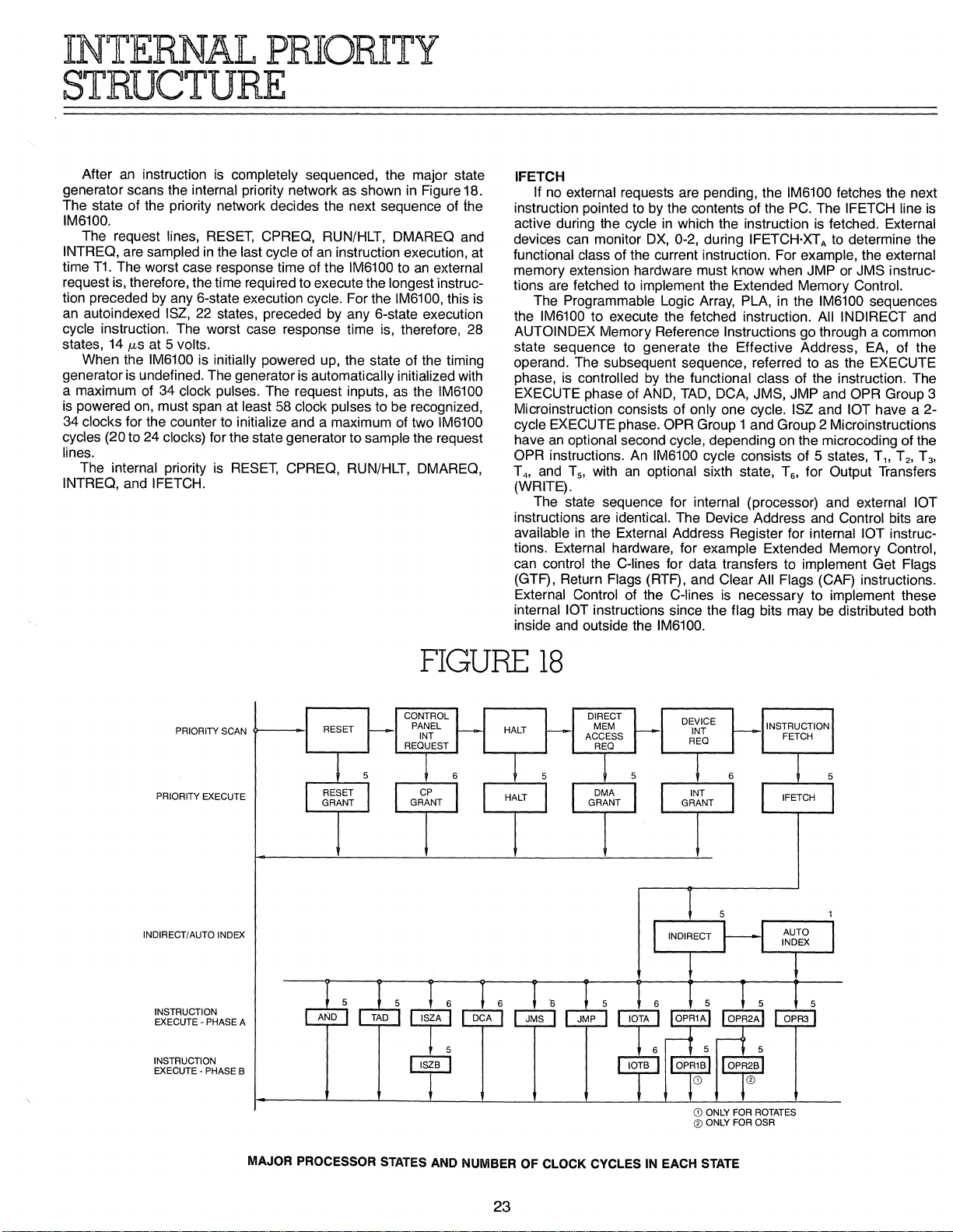
After
an
generator scans the
The state of the priority network decides the next sequence of the
IM6100.
The request lines,
INTREO, are sampled
time
T1.
request
tion preceded
an
autoindexed
cycle instruction. The worst case response time
states,
When the
generator
a maximum
is
powered on, must span
34
clocks for the counter
cycles (20 to
lines.
The internal priority
INTREO,
instruction
The worst case response time of the
is,
therefore, the time required to execute the longest instruc-
by
ISZ,
14
fLs
at 5 volts.
IM6100
is
undefined. The generator
of
34 clock pulses. The request inputs,
24
clocks) for the state generator to sample the request
and IFETCH.
is
completely sequenced, the major state
internal priority network
RESET,
in
any 6-state execution cycle. For the
22
is initially powered up, the state
is
CPREO, RUN/HLT, DMAREO
the last cycle
states, preceded
at
least
58
to
initialize and a maximum
RESET,
CPREO, RUN/HLT, DMAREO,
as
shown
of
an
instruction execution, at
IM6100
by
any 6-state execution
is
automatically initialized with
clock pulses to
in
to
IM6100,
is,
therefore,
of
as
the
be
recognized,
of
two
Figure 18.
an
external
this
the timing
IM6100
IM6100
and
28
IFETCH
If
no
external requests are pending, the
instruction pointed
active during the cycle
devices
functional class of the current instruction. For example, the external
memory extension hardware must know when JMP or JMS instruc-
tions
is
the
AUTOINDEX Memory Reference Instructions
state sequence to generate the Effective Address,
operand. The subsequent sequence, referred
phase,
EXECUTE phase
Microinstruction consists of
cycle EXECUTE phase.
have
OPR instructions.
T
(WRITE).
instructions are identical. The Device Address
available
tions.
can control the C-lines for data transfers to implement Get Flags
(GTF), Return Flags (RTF), and Clear All Flags (CAF) instructions.
External Control of the C-lines
internal lOT instructions since the flag bits may
inside
can
are
fetched to implement the Extended Memory Control.
The Programmable Logic
IM6100
is
controlled
an
optional second cycle, depending
4,
and
T
5,
The state sequence for internal (processor)
in
External hardware, for example Extended Memory Control,
and
outside the
to
by
the contents of the
in
which the instruction
monitor
to execute the fetched instruction. All INDIRECT and
with
the External Address Register for internal lOT instruc-
OX,
0-2, during IFETCH·XTA to
Array,
PLA, in the
by
the functional class
of
AND,
TAD,
DCA,
only one cycle. ISZ and lOT have a 2-
OPR Group 1 and Group 2 Microinstructions
An
IM6100
an
optional sixth state, T
IM6100.
cycle consists of 5 states, T
is
necessary to implement these
IM6100
PC.
JMS, JMP
on
fetches the next
The IFETCH line
is
fetched. External
IM6100
go
through a common
to
as
of
the instruction. The
and
the microcoding of the
6,
for Output Transfers
and
and
be
the EXECUTE
Control bits are
distributed both
is
determine the
sequences
EA,
of the
OPR Group 3
,
T
2, T 3,
1
external lOT
PRIORITY SCAN
PRIORITY EXECUTE
INDIRECT/AUTO INDEX
INSTRUCTION
EXECUTE·
INSTRUCTION
EXECUTE· PHASE
PHASE A
B
1>---1
RESET
FIGURE
HALT
~
18
5
G8
6
1
I
lor
6
T
DEVICE
INT
REO
GT
5
IOTBI
IOTBI
CD
CD
ONLY FOR
CD
ONLY FOR OSR
6
5
5
CD
T
ROTATES
MAJOR PROCESSOR STATES AND NUMBER OF CLOCK CYCLES IN EACH STATE
23
Page 25
INTERNAL
PRIORITY
STRUCTURE
CONTINUED
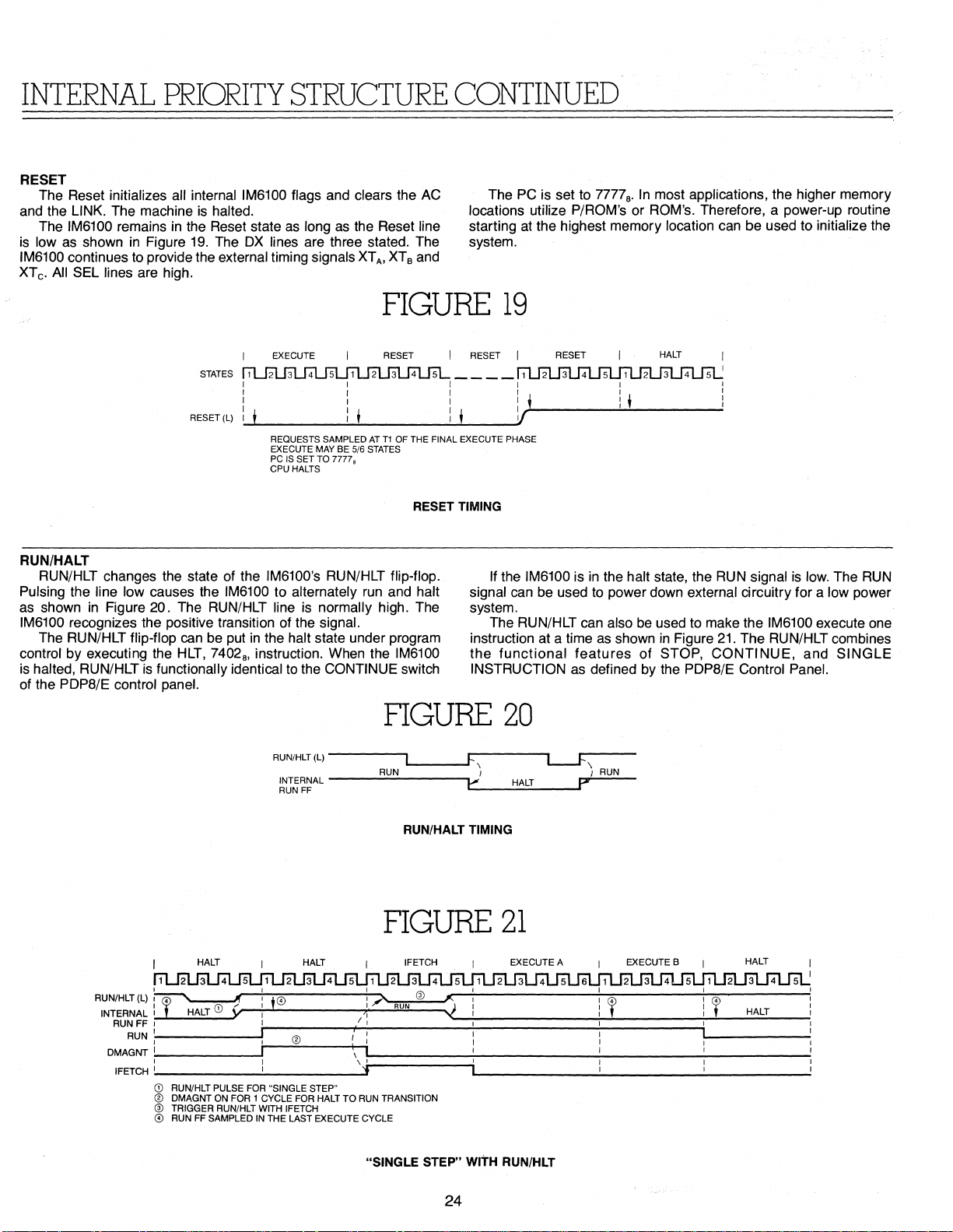
RESET
The Reset initializes all internal IM6100 flags and clears the
and the LINK. The machine
IM6100 remains
The
is
low
as
IM6100 continues
shown
XT
c.
All SEL lines are high.
in
Figure
to
provide the external timing signals XT
is
halted.
in
the Reset state
19.
The
as
long
as
the Reset line
OX
lines are three stated. The
A
,
XT Band
FIGURE
EXECUTE RESET RESET
STATES
~
RESET (L)
__________
REQUESTS SAMPLED
EXECUTE
PC
IS
SET TO 7777"
CPU HALTS
RUN/HALT
RUN/HLT changes the state of the IM6100's RUN/HLT flip-flop.
Pulsing the line low causes the
as shown
IM6100
in
Figure 20. The RUN/HLT line
recognizes the positive transition of the signal.
The RUN/HLT flip-flop can be put
control by executing the
is halted, RUN/HLT
of the POP8/E control
HLT,
is
functionally identical
panel.
IM6100
7402
to alternately
in
the halt state under program
,
instruction. When the
8
to
r I r r
:
~: ~,
__________
AT
MAY BE 5/6
is
normally high. The
the CONTINUE switch
STATES
run
T1
and halt
AC
The PC is set
locations utilize P/ROM's or ROM's. Therefore, a power-up routine
starting
at
system.
19
____
::
~: ~1
____
OF THE FINAL EXECUTE PHASE
RESET TIMING
signal can
system.
IM6100
instruction at a time
the
INSTRUCTION
1
~1~----------~--------~
If
the IM6100 is
The RUN/HLT can also
functional
7777
.
In
most applications, the higher memory
8
to
the highest memory location can be used to initialize the
RESET
HALT
tit
in
be
used
to
power down external circuitry for a low power
be
used to make the IM6100 execute one
as
shown
features
in
of STOP,
as defined by the POP8/E Control Panel.
the halt state, the
Figure
CONTINUE,
RUN
signal
is
low.
21.
The RUN/HLT combines
and SINGLE
The
RUN
FIGURE
RUNIHLT (L)
INTERNAL
RUN
--------"""L
---':":'::';~---""'P"
FF
____
RUN I I RUN
----'r-F-\
RUN/HALT TIMING
FIGURE
HALT HALT
RUNIHLT (L)
INTERNAL : HALT
~
RUN FF I / :
RUN r I I
I
DMAGNT~:;-C_C_C_C_C_C_C_C_C_C_~=L
IFETCH
~
CD
RUN/HLT PULSE FOR "SINGLE STEP"
® DMAGNT ON FOR 1 CYCLE FOR HALT
® TRIGGER RUN/HLT WITH IFETCH
® RUN FF SAMPLED
If,---!--,-,,,......----...:----.
CD
r
® I I
_____
IN
THE LAST EXECUTE CYCLE
~:\j!~::::::::::i:[[[[[[[[[[[[[[c=[[[[[[[[[[J[[[[[[[[[[[~
TO
IFETCH EXECUTE A EXECUTE B
j
RUN TRANSITION
"SINGLE STEP" WITH RUN/HLT
20
-------.L-F\
HALT P
21
HALT
24
Page 26

PDP-8/E
COMPATIBILITY
The
are software
system supplied
erly with
Loaders, PAL
Technique (DDT),
Point Package
execute the complete set
subset
programmed I/O interfaces for the PDP-8E, for example, Teletype,
Papertape Reader/Punch, etc., will operate with the IM6100 without
any hardware or software modification.
PDP-8/E are different, the
PDP-8 1-CYCLE BREAK, but not
IM6100
Since the bus structure
of
The Direct Memory Access,
and the PDP-8/E*
compatible. The basic PDP-8/E paper-tape software
by
the
the PDP-8/E OMNIBUS* signals,
Digital Equipment Corporation will operate prop-
IM6100.
This basic software package includes Binary
III
Assembler, Symbolic Editor, Dynamic Debugging
Octal Debugging Technique (ODT),
and
FOrmula CALculator (FOCAL)*. The IM6100 will
of
of
of
Digital Equipment Corporation
CPU
diagnostics for PDP-8/E.
the
IM6100
DMA,
IM6100
can
be
as
structure of the
DMA structure
compatible.
adapted
shown
23
Bit Floating
to
in
Figure
IM6100
is
similar to the
provide a
22,
and
FIGURE
INTERSIL
IM6100
LXMAR
P4>
DX
XTA
DEVSEL(L)
XTC
CO.
C1.
SKP.
]oc»--
-
1
INT
(L)
!l>...
IV'
TS
Ic
~
XMAR
:0
V
1 "
--/
The IM6100 handles 4K words of memory directly. Like the
PDP-8/E,
used to extend the addressing space up to 32K. All necessary
control
troller
processor options of the PDP-8/E cannot
The EAE
timesharing.
all
with certain special features. The Control Panel has a dedicated INT
request line to the
in
a separate memory, distinct from the normal program memory.
The
user and the user program can occupy the entire 4K of main
memory. The bootstrap routines may
control panel memory. Unlike the PDP-8/E, the IM6100 bootstrap
routines
common address space.
an
external Extended Memory Control element
and
timing signals
are
generated by the
The Extended Arithmetic Element, EAE, and the User Flag,
is
used for hardwired Multiply/Divide and the UF for
The
IM6100
control panel service routine
tre?ts the Control Panel
IM6100
and
the loaded user programs, can, therefore, share
to
implement the memory extension con-
IM6100.
be
used with the
as
a programmed I/O device
and the control panel program
can
be
made transparent to the
also reside
in
22
MD(L)
+5
DATA(L)
PDP 8/E
TELETYPE
INTERFACE
+5
f
CO.
10 PAUSE
C1,
SKP,
INT
(L)
TP3
(L)
can
the
dedicated
can
be
UF,
IM6100.
reside
'Trademarks
EXAMPLE OF A PDP-alE PROGRAMMED
of Digital Equipment Corporation
25
1/0
PERIPHERAL INTERFACE
1 RDR RUN
DATA
OUT
DATA
IN
TTY
Page 27
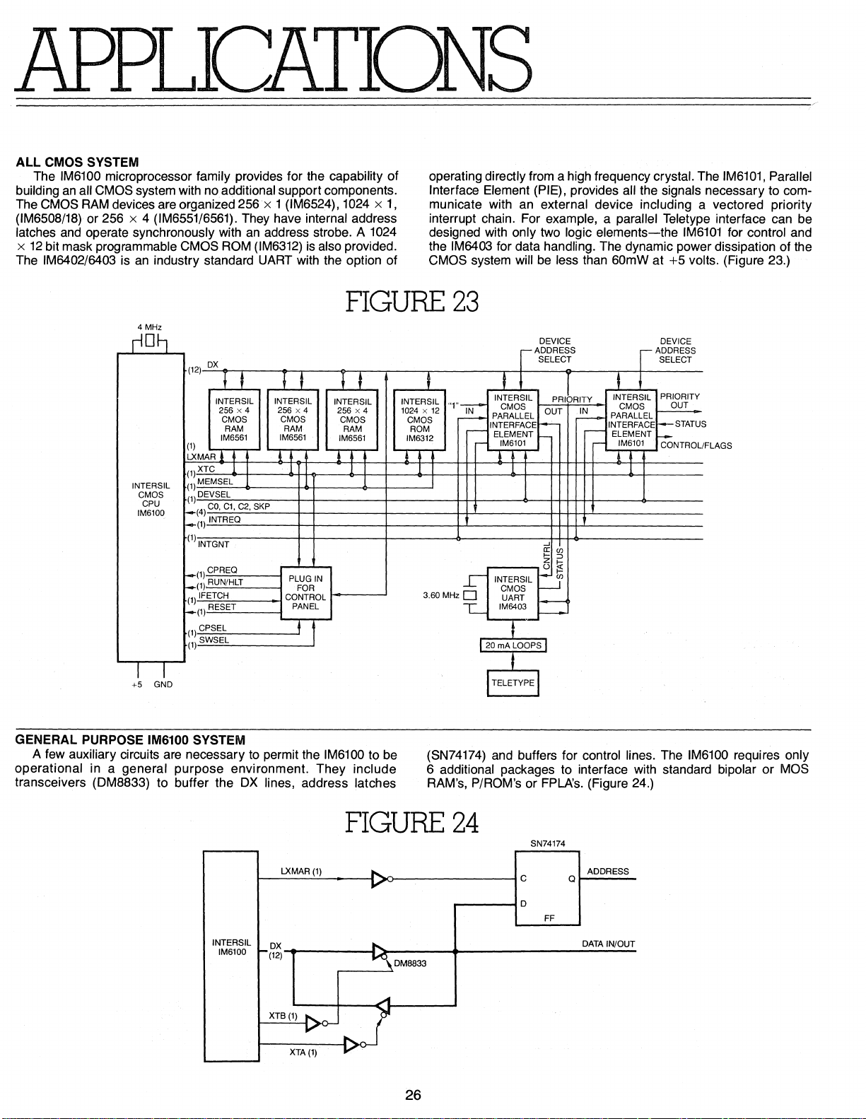
APPLICATIONS
ALL CMOS SYSTEM
The
IM6100
building
The
an
CMOS
(IM6508/18) or 256 x 4 (IM6551/6561). They have internal address
latches
The
and
x
12
bit mask programmable CMOS
IM6402/6403 is
microprocessor family provides for the capability of
all CMOS system with no additional support components.
RAM
devices are organized 256
operate synchronously with
an
industry standard UART with the option of
xi
an
address strobe. A
ROM
(IM6312)
(IM6524),
is
also provided.
1024
xi,
1024
operating
Interface Element (PIE),
municate with
interrupt chain. For
designed with
the
CMOS system will
directly from a high frequency crystal. The
provides all the signals necessary to com-
an
external device including a vectored priority
example, a parallel Teletype interface can be
only two logic
elements-the
IM6403 for data handling. The dynamic power dissipation of the
be
less than 60mW at
IM6101,
IM6101
+5
for control and
volts. (Figure 23.)
Parallel
4
MHz
rD~
INTERSIL
CMOS
CPU
IM6100
I I
+5
GND
(12)
DX
f J t t
INTERSIL INTERSIL
256 x 4 256 x 4
CMOS CMOS
RAM RAM
IM6561
(1)
LXMAR 1 • •
(1)XTC 1 I
(1)MEMSEL 1
(1)DEVSEL
_(4)
co,
C1,
-0-(1) INTREQ
(1)INTGNT
_(1)CPREQ
'-(1)
RUN/HLT
(1)
IFETCH
~(1)RESET
(1)
CPSEL
(1)
SWSEL
C2,
IM6561
t + .•
SKP
1 I
1
PLUG
IN
FOR
CONTROL
PANEL
+
FIGURE
INTERSIL
x 4
256
CMOS
RAM
IM6561
! • •
1 I
INTERSIL
1024 x 12
CMOS
ROM
IM6312
! • +
1 I 1 1
1
23
t t
"1
I
MHz 0
3.60
INTERSIL
" --::-:---
PARALLEL
~
INTERFACE
- -
ELEMENT
r-
INTERSIL :..J
...L
""L-
120
TELETYPE
[_ADDRESS
~
CMOS
IM6101
i •
CMOS
UART
IM6403
t
rnA
LOOPS I
I
DEVICE
SELECT
PRIR,TY
OUT
--'-
-
--'
a:
Ul
f-
::::J
13
~
-
-
~
-
[ADDRESS
t
+
INTERSIL
CMOS
PARALLEL
INTERFACE
ELEMENT
IM6101
t •
DEVICE
SELECT
PRIORITY
OUT
:--STATU
rcoNTROL!
S
FLAGS
GENERAL PURPOSE IM6100 SYSTEM
A few auxiliary circuits
are
necessary
to
permit the
IM6100
to
be
operational in a general purpose environment. They include
transceivers (OM8833) to buffer the
OX
lines, address latches
FIGURE
INTERSIL
IM6100
DX
-(12)
"''''I
LXMAR(1)
XTA
po-J
(1)
......
~\DM8833
.A
(SN74174)
and
buffers for control lines. The
IM6100
6 additional packages to interface with standard bipolar or
RAM's, P/ROM's or
FPLA's.
(Figure 24.)
24
SN74174
C
D
FF
26
Q
ADDRESS
DATA
IN/OUT
requires only
MOS
Page 28
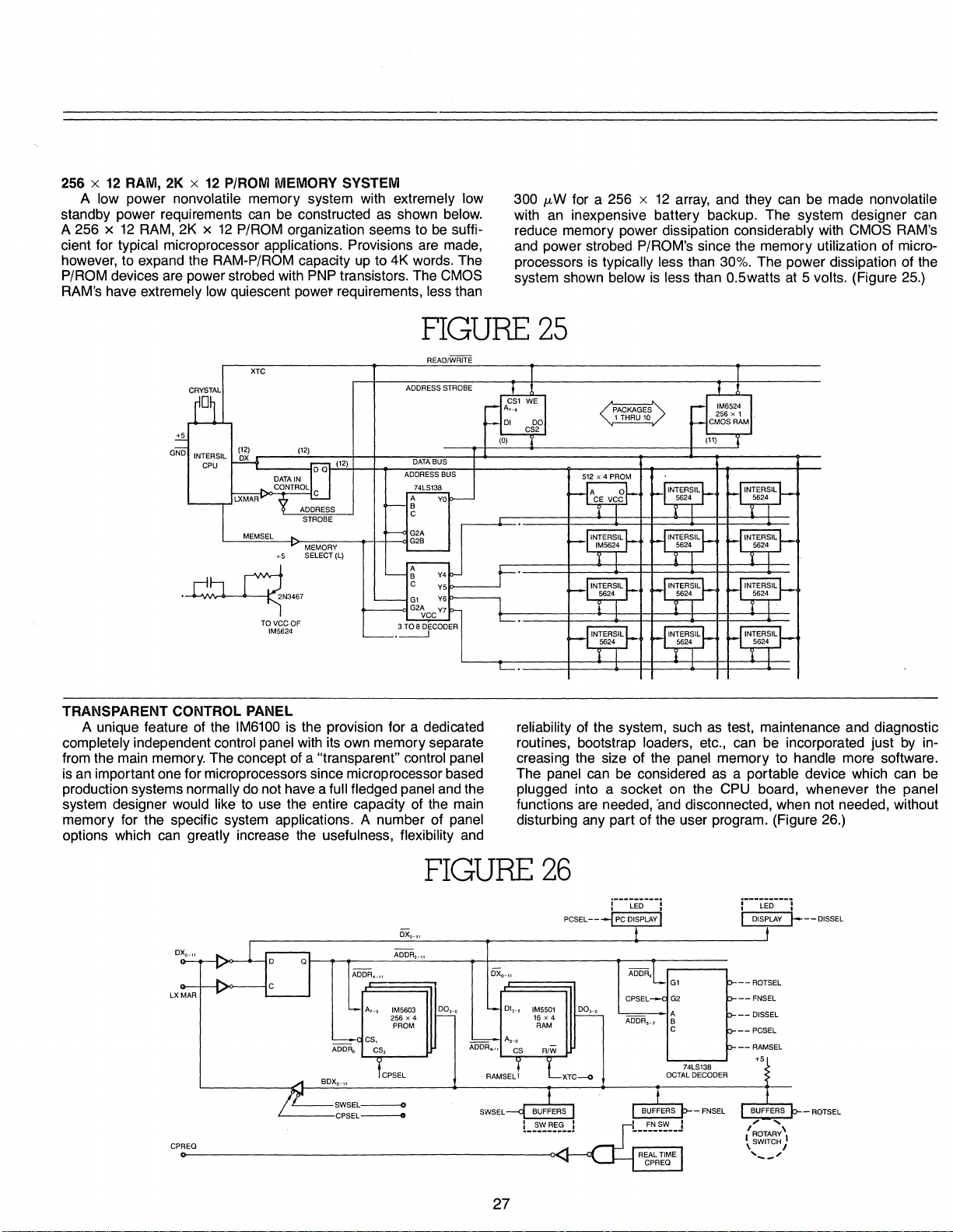
256 x
12
RAM, 2K x
12
P/ROM MEMORY SYSTEM
A low power nonvolatile memory system with extremely low
standby power requirements can be constructed as shown below.
A 256 x
cient for
12
RAM, 2K x
12
P/ROM organization seems to be suffi-
typical microprocessor applications. Provisions are made,
however, to expand the RAM-P/ROM capacity up to 4K words. The
P/ROM devices are power strobed with PNP transistors. The CMOS
RAM's have extremely low quiescent power requirements, less than
300
/-LW
for a 256 x
12
array, and they can be made nonvolatile
with an inexpensive battery backup. The system designer can
reduce memory power dissipation
and power strobed P/ROM's since the memory
is
processors
system shown
typically less than 30%. The power dissipation of the
below
is
less than 0.5watts
considerably with CMOS RAM's
utilization of micro-
at
5 volts. (Figure 25.)
FIGURE
XTe
(12)
TO vee
OF
IM5624
TRANSPARENT CONTROL PANEL
A unique feature of the IM6100 is the provision for a dedicated
completely independent control panel with its own memory separate
from the main memory. The concept of a "transparent"
is
an important one for microprocessors since microprocessor based
production systems
system designer
memory for the specific system
normally do not have a full fledged panel and the
would like to use the entire capacity of the main
applications. A number of panel
options which can greatly increase the usefulness, flexibility and
READ/WAITE
ADDRESS
STROBE
DATA
BUS
ADDRESS
BUS
74LS138
A
YO
8
e
G2A
G28
A
Y4
8
e
Y5
Y6
Gl
G2A Y7
vee
3
TO
8 DECODER
.--..J
control panel
25
reliability of the system, such as test, maintenance and diagnostic
routines, bootstrap
creasing the size of the
The
panel can be considered as a portable device which can
plugged into a socket on the CPU board, whenever the panel
functions are needed,
disturbing any part of the user program. (Figure 26.)
loaders, etc., can be incorporated just
panel memory to handle more software.
'and
disconnected, when not needed, without
by
inbe
ep:-EQ-------
ADDR
________________
Ar_o
es,
..
_
11
CPSEL
FIGURE
DX
-
o
I1
ADOR
_"
e
IM5603
256
PROM
DOH
x 4
26
i---lEO---i
PCSEL--
_
DX
11
O
01
IM5501
H
16 x 4
RAM
74LS138
OCTAL
DECODER
SWSEL BUFFERS
: SWAEG : I FNSW :
p-
-FNSEL
--_-_---<-~-:~~~;;:1
27
i
DISPLAY
--
ROTSEl
--
FNSEL
--
D1SSEL
--
peSEL
--
RAMSEL
+5
,..
I \
I
ROTARY
\
SWITCH
'-_.II'
i-
--
DISSEL
-ROTSEl
"
I
I
Page 29
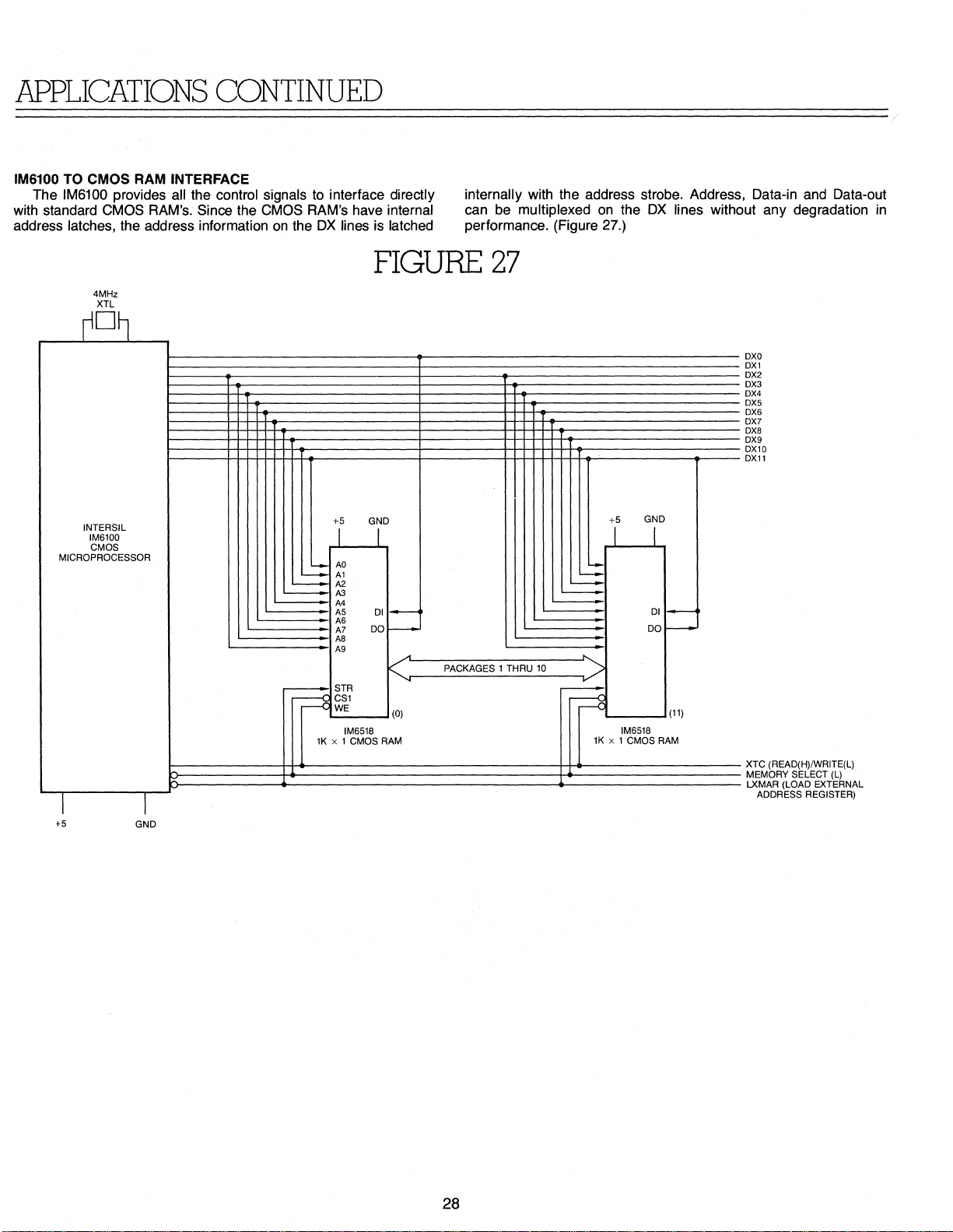
APPLICATIONS
CONTINUED
IM6100 TO CMOS RAM INTERFACE
The IM6100 provides
with
standard CMOS RAM's. Since the CMOS RAM's have internal
address latches, the address information
4MHz
XTL
D
r
1
INTERSIL
IM61DD
CMOS
MICROPROCESSOR
I
I
GND
all
the
control
signals
on
the
~
P
to
interface directly
OX
lines
+5
I I
AO
--=:
Al
A2
A3
A4
A5
A6
A7
A8
A9
STR
CSl
WE
IM6518
lK
x 1 CMOS RAM
internally
can be
is
latched
performance. (Figure 27.)
FIGURE
GND
DII-
DO
f--
<
(0)
PACKAGES 1 THRU 10
multiplexed
27
with
the address strobe. Address, Data-in and Data-out
on
the
OX
lines without any degradation
DXO
OXl
OX2
OX3
OX4
OX5
OX6
OX?
OX8
OX9
OX10
OX11
GND
+5
I I
t..-
-=:
-
DO
DI
-
-
>
--;:::8
lK
IM6518
x 1 CMOS RAM
(11)
XTC
(READ(H)/WRITE(L)
MEMORY SELECT (L)
LXMAR
(LOAD EXTERNAL
ADDRESS
REGISTER)
in
28
Page 30
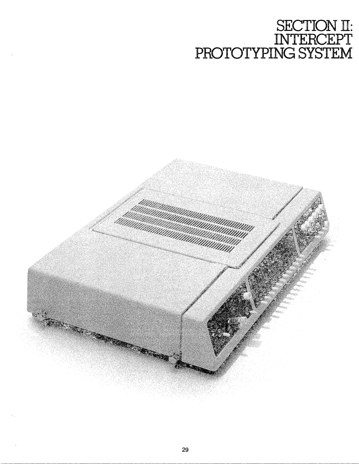
SECTIONll:
INTERCEPT
PROTOTYPING
SYSTEM
29
Page 31

INTRODUCTION
INTERCEPT
of
prototyping
of
devices
bench
or
desk
2-7/8"
IM6100
state
memory
plied
INTERCEPT
design
flexibility
processor
RAM,
and
microprocessor.
TTL
operation.
by
Digital
features
in
Standard
to
6901-M4KX12,
user
in
typical
top
operation,
precisely
compatible
Equipment
without
of
the
developing
PDP-8
have a
provides
systems
configurations.
duplicates
The
any
Control
and
is
The
simplified
and
fully
basic
PDP-8/E*
Corporation
software
prototyping
both
software
programs
Panel,
and a PDP-8/E
you
an easy
evaluating
INTERCEPT,
di
mensioned
the
functions
buffered,
or
hardware
system
and
require
6900-CONTR
compatible
economical
the
10-3/4" X 16-1/2"
and
bus
structure,
eases I/O
papertape
will
operate
modifications.
give
the
hardware.
the
IM6100
L,
IM6100
packaged
timing
being
handling
software
properly
user
complete
4K
words
Teletype
means
family
for
X
of
the
three-
and
sup-
with
The
micro-
of
inter-
face,
6902-CPUTTY -the
Four
72
pin-36
bus
(Figure A).
fourth
under
INTBUS,
25
at
type
permitting
to
committing
figuration.
is
provided
the
unit
the
position
the
generate
pin
back
of
interface
1.0
With I NTE RCEPT,
and
to a masked
basic
position
The
(Figure
Universal Bus.
and
the
(Figure C). A 5
amps
test
edge
basic
modules
as a user
B)
socket
case, as well as a 9
for
user
user
programs
ROM
modules
connectors
utilize
option.
for
user
Two
Amplimite
connectors
volt, 3 amp
option
the
user has a fully
and
pattern
provided
are
three
Access
options
are
provided,
position
power
modules.
peripheral
and
in
provided
connectors
to
the
or
for
attaching
High
connector
supply
interactive
interfaces
a final
INTERCEPT.
on a common
and
bus
is
available
6904-
Density
20
uncommitted,
for
is
provided
facility
before
hardware
the
CD,
tele-
con-
Figure
Figure
A_
B.
*Trademark
G)
AMP
INC.,
Digital
Equipment
Harrisburg,
PA
Corp.
Figure
C_
30
Page 32

MEMORY
ORGANIZATION
NONVOLATILITY
CLOCK
INPUT
OUTPUT
POWER REQUIRED
DIMENSIONS
RATE
SIGNALS
SIGNALS
6901-M41<X12
6901-M4KX12
6901-M41<X
ALL
ALL
ALL
6900-CONTRL
6901-M4KX
6902-CPUTTY
6900-CONTR
6901-M4KX12
6902-CPUTTY
ALL
6900-CONTR
12
12
CARDS
1024 x 1 CMOS Static RAM - IM6508
x
12
4096
40
4 MHz
TTL
TTL
900
DC
5 ±
3 Amps at
AC
105-125 or
45 Watts Max. at Full Load Rating
400
700
L
10-3/4" x 16-1/2" x 2-7/8"
6" x 8-1/2" x 3/4"
6"
72~Pin-36
L
Four 72
Pin-to-PinSpacing
- Four 1024 x 12 Arrays
Days
@ 25°C
Compatible
Compatible
mA@5 V DC
Output
x
of
Power Supply
5%
Volts
40°C
Input
210-250
mA@5 V DC
mA@5 V DC
8-1/2" x 3/4"
Position,
c
Pin - 36 Position Sockets,
0.100"
Volts at
57-63
Pin-to-Pin Spacing
0.100"
Hz
I
6901:M4KX12
4096X
NONVOLATILE
CMOS
12
RAM
INTERCEPT PROTOTYPING SYSTEM
PARALLEL
TELETYPE
INTERFACE
INTERCEpT
6900-CO NTR L
6903-CONTR
CONTROL
PANEL
BUS
L-1
I
I
I 6904-INTBUS
I
r-----------,
I I
: USER i
I
I I
I I
INTERFACE
I
L----r----J
,,---
......
_--'"
......
/ ,
I \
I USER \
I SYSTEM ,
\ I
, I
" /
31
Page 33

6900-CONTRL
INTERCEPT
CONTROL
The
6900-CONTRL
INTERCEPT
CONTRL
1,
is
a PC
into
the
case
and
switches
maintenance.
connected
flat
cable.
examine
and
display internal processor
execute
except
is
organized
board
6900
bus.
front
and
The
to
the
The
The
operator
and
modify
machine
which
The
panel
indicators
logic
control
control
language
PANEL
consists
6901-M4KX12
in
two
modules:
contains
second,
of
INTERCEPT,
and
panel
may
the
logic
6903-CONTROL-2,
to
facilitate processor
memory
panel
module,
module
start
and
contents
operation,
programs
MOD1JLES
of
all
the
component
and
6902-CPUTTY.
The
first,
6903-CONTROL-
and
which
card,
6903-CONTR
requires
stop
of
the
or
memory
main
bootstrap
and
is
consists
contains
6903-CONTRL-1,
900
program
manually
an
operation
L-2,
mA
at
execution,
memory,
and
load
parts
6900-
inserted
of
the
array
and
with
5 V
DC.
modify
and
execute
programs
of
microprocessor
externally,
information
program
16 x 12
of
completely
is
processor
a
displayed
with
is
provided
Operator
via
the
Teletype
register
the
must
resides in
RAM-256 x 12 P /ROM.
transparent
Provisions are
operation.
in
real time_
the
"USER
Additional
in
Console".
and
modification
be
done
the
to
made
The
The
FN"
switch.
information
Applications
or
a high
internal
and
under
console
the
user.
for
single
processor
user
defined
Bulletin M006
speed
control
display
program
memory
The
instruction
state
on
the
tape
reader.
signals
of
internal processor
control.
which
console
information
routines
are
6900-CONTR L module
entitled
Since
are
not
available
The
is
organized as
operations
and
single
can also be
implemented
"IM6100
console
clock
the
are
Figure
D.
Figure E.
32
Page 34

MODULES
6901-M4KX12
4096 X
CMOS
The
sists
of
48
CMOS
49152
memory
decoded
provision
as
memory
battery
automatically
battery
the
the
and
provided
Systems
ordered
bits
expansion
and
enables
"read-only"
may
back-up
voltage falls
retention,
module
memory
it
from a "live"
is
dimensioned
Additional
in
For
by specifying
of
buffered
even
power
module
Appl ications Bulletin
12
NONVOLATILE
MEMORY
4096 x 12
random
the
to
be
write
guarantees
recharged
momentarily,
system.
the
IM6100". A blank
nonvolatile
static
RAMs (lM65081. providing
access
by utilizing
for
TTL
user
to
simulate
protected.
when
below
is
restored. A switch
from
stray
The
6" x 8-1/2" x 3/4".
information
the
number
MODULE
memory.
the
Field
compatibility.
block
the
RAM-ROM
The
data
retention
the
the
level
an LED
signals
module
on
the
M004
6901.
CMOS
memory
The
module
Select
The
upper
31<
configurations.
500mAH
up
to
module
required
requires
printed
is
indicator
is
provided
when
inserting
400mA
6901-M41<X12
entitled
circuit
module
the
provides
input
and
31<
Write
words
of
The
Nickel
40
days
powered.
to
guarantee
illuminates
to
or
at
"Static
board
con-
user
with
for
is
fully
Protect
memory
entire
Cadmium
and
If
the
data
when
protect
removing
5 V DC
module
Memory
can
be
•
f •
is
is
Figure F.
•
6902-CPUTTY
IM6100/TELETYPE
The
6902-CPUTTY
three-state
the
parallel
with
define a TTL
control
wire-ANDing
stated
permitting
access
for
crystal
clock
between
reader
Transmitter,
In
view
PDP-8
The
CDTrademark -Teletype
@Trademark -Digital
bus-organized
IM6100
standard
prototyping,
externally.
serial
microprocessor
Teletype
All
signals have pull-up resistors
when
memory
Since
controlled
The
the
and
of
software
interface.
high
compatible
IM6100 signals
of
the
the
IM6100
the
peripheral device,
using
the
6902-CPUTTY
provisions are
oscillator
Gating
module
IM6100
printer/punch.
UART,
the
fact
will
data
formatting
current
request
the
contains
and
is
that
operate
Corporation
Equipment
module
prototyping
with a DEC@
The
microprocessor
three-state
bus.
are
lines.
grants a Direct
same
bus
made
and
is
provided
the
an
ASR-3320-3JC
A Universal
provided
the
interface
properly
is
RS-232
Corporation,
for
available
The
which
lines as
module
to
to
required
CD
MODULE
forms
the
nucleus
system.
introduce a TTL
ensure
parallel-serial
is
compatible
The
PDP-8/E
signals are
buffers
to
without
and
externally.
permit
memory
Memory
requested
the
processor.
will be
to
stop
the
integral clocking.
logic
Teletype
Asynchronous
PDP-8/E
compatible,
any
and
Maynard,
module
transceivers
open
signals
Access
principally
to
data
MA
of
the
contains
compatible
buffered
to
The
input
collector
are
three-
request
the
DMA,
to
used
free
running
compatible
transfer
modification.
the
data
keyboard/
Receiver/
formatting.
DEC
interface
33
provides
5 V DC
provided
face
For
circuit
board
for
20mA
and
is
dimensioned
Additional
in
Applications
the
IM6100 CMOS
can
current
information
be
ordered
G.
Figure
loops.
The
module
6" x 8-1/2" x 3/4".
on
the
6902-CPUTTY
Bulletin M005
Microprocessor". A blank
by
specifying
entitled
the
number
requires
"Teletype
700mA
module
6902.
at
is
Inter-
printed
Page 35

SOFTWARE
AND
HARDWARE
The
packages
6904-
as
Position
3' x 2"
6904-INTBUS
supply
are
INTBUS
The
defined in
connectors
Flat Flexible Cable
for
the
following
also available
6904-INTBUS
Appendix
to
6904-INTBUS
additional hardware modules and software
from
UNIVERSAL
shown in Figure H
1.
The panel provides
with
1-1/4"
INTERCEPT
OPTIONS
Intersil Inc.
connector
is
provided to
for
is
user supplied.
6905-WIREWP
UNIVERSAL
WIREWRAP
The Universal Wirewrap module shown in Figure I permits
the user
system. The module provides
spacings.
to
prototype
MODULE
and incorporate user interfaces
for
all standard dual in line pin
BUS
has
a bus structure
for
eight 72 Pin-36
to
connector spacing. A
permit
user expansion. The power
attaching the
to
the 6900
Figure
H.
6906-EXTEND
EXTENDER
The Extender module shown in Figure J enables the user
to
extend any 6900 card
and debugging.
MODULE
for
6907-EMC
EXTENDED
MEMORY
CONTROLLER
The
permits
K
words.
the
user
6907-EMC
Module
of
INTERCEPT
6909-RRELAY
READER
This
reader
surges
ING SYSTEM.
control
when
RELAY
2Y:z"
x 3%"
and
protection
interfacing
PC
ASR33
servicing, testing, trouble-shooting
MODULE
together
to
card
provides a means
against
to
with
the
6904-INTBUS
expand
the
memory
noise
induced
the
INTERCEPT PROTOTYP-
for
up
remote
by
to
Figure I.
32
Figure J.
line
34
Page 36

EXTENDED
SOFTWARE
FOCAL-8*
PACKAGE
The
basic
PDP-8/E
in
creating
programs
on
the
entitled
PDP-8/E
DOCUMENTATION
Small
PDP-8
Introduction
PDP-8
4K
assemblers
Self-starting
BINARY
Self-starting
PAL
DDT'
ODT
ODT
Symbolic
RIM
OCTAL
Binary
PDP-8
RIM pa
Binary
and
after
software
"IM6100
EXTENDED
computer
pocket
to
family
binary
PAPERTAPES
binary
III
(LOW)
(HIGH)
editor
punch
ASR
memory
punch
23
BIT
perta
pes
loader
editing
assembly
is
CMOS
handbook
reference
programming
commonly
PAL
111/MACRO-8
loader
loader
33
high
dump
ASR
33
floating
6982-QF081-AC
papertape
programs
or
compilation_
provided
Microprocessor
SOFTWARE
(8E,
card
used
(PDP-8E, 8M,
memory
point
package
in
utility
and
the
8F,
software
in
debugging
Additional
Applications
Basic
KIT
8M)
routines
8F
only)
kit
Software"_
assists
and
correcting
information
Bulletin
the
user
M003
(6982-
FOCAL-8
desk
calculator
power
of
the
sentence
BASIC,
more
capability
on-line
gramming
Teletype.
extendable
FOCAL-8
Document
Binary
Listing
FOCAL-8
Binary
Listing
FOCAL-8
Binary
Listing
structured
ALGOL
easily
problem
Papertape
papertape
papertape
IS-
LFOCA)
is
an
mode
of
processor
keyboard
and
FORTRAN
learned.
and
language.
Yet,
I/O
remove/replace
8K
simplicity
solving
it
offers
and
versatile
overlay
The
FOCAL
(8/E)
interactive
operation
available
commands.
dynamic
makes
without
requires
a full range
self-editing
algebraic
makes
to
the
user
in
many
combination
FOCAL-8
having
to
only
of
capabilities.
language.
the
full
computational
in
response
FOCAL
respects.
an
master a complex
4K
words
mathematical
is
However,
of
computational
ideal
language
of
RAM
FOCAL's
to
simple
similar
functions,
to
it
for
pro-
and
is
a
DIAGNOSTIC
6985-IDIAG-l
Th
is
extensive
tests
software
on
the
package
processor,
SOFTWARE
consists
memory
of
programs
and
the
Teletype.
KIT
to
perform
6981-FOPAL-ill
PAL-ill
CROSS
FORTRAN.
PDP-8/E
Package.
FORTRAN.
'Trademark
35
FORTRAN
ASSEMBLER
FOPAL-III
The
cross
PAL-III
It
will
Digital
Assembler,
run
Equipment
is
a cross
assembler
on
any
supplied
computer
Corp.
assembler
is
functionally
with
installation
written
the
in
identical
Extended
that
standard
to
the
Software
supports
Page 37

6970-IFDOS
INTERCEPT
OPERATING
DESCRIPTION
The
6970-IFDOS
designed
microprocessor-based system.
ASR33 is required,
(included
HARDWARE
two
all electronics,
over
the
contained
mountable
module
is
connected
ribbon
Features:
• IBM 3740
•
Software
minicomputers
•
Intelligent
cations
• Detect, identify, and correct errors resulting
•
•
Automatic
performed
•
Flexible
require
the
to
facilitate
with
the INTERCEPT
The
hardware
completely
four
(4)
million
INTERCEPT
in a
or
can be placed
is
inserted
cable.
compatible
compatible
disc
which
electrical,
Completely
storage
media
transparent
at
Programmed
direct
system
power
to
times
FLOPPY
SYSTEM
Floppy
development
An
as
well
as
at
prototyping
components
interfaced
prototyping
single
the
drive/controller
provide
format a diskette
communications
supplies,
bits
of
directly
disc
media
the
or
human
self
when
covered
floppy
"on
line"
system.
on
into
system
with
with
ability
tests on disc related
system
Input/Output
Disc
of
ASCII
least
of
disc
and
cables necessary
mass
enclosure
any
flat
the
multiple
DEC RX8
formatter/interface
to:
malfunction
within
throughput
between
DISC
Operating
software
terminal
4K
words
system).
6970-IFDOS consist
drive
storage
All
surface. The interface
INTERCEPT
via a multi-conductor
sources
industry
for
applications
user
System
for
an IM6100
such
as
of
memory
mechanisms
to
capability
components
which
for
from
is least affected
is
bus
the
PDP-8
communi-
mechanical,
standards
equipment
programs
the
with
add
are
rack
and
are
that
and
SOFTWARE
is
Features:
• A
file
system
disc
and
performs
as specified
• A keyboard
the
user
commands
of
to
transfer
user
file
•
An
easy
and
modify
•
An
extremely
source
output
• A
binary
files and facilitates
•
An
octal
and
control
•
Numerous
dumping
system parameters, and
DIAGNOSTIC SOFTWARE
•
Binary
• A
listing
PHYSICAL SPECIFICATIONS
• DIMENSIONS
• WEIGHT 54 Ibs
• POWER REQUIREMENTS
The
software
arately
6980-ISOFT can be
The
Diagnostic
ing
6985-IDIAG-3.
monitor
and
files between
catalog, and call
to
learn
ASCII
programs
for
subsequent
loader
debugger
execution
utility
of
programs
of
the
component
by
specifying
which
maintains
file
handling
by
user
which
the
operating
to
enter
and
memory
system
text
editor
text
at
the
fast
and
flexible
created
which
which
programs
floppy
to
programs
Height
Width
Depth 22.5 inches
110
volts
2.0
Amps
ordered
Software
by
loading
loads
loading
allows
of
programs
discs,
printing
test
the
10.5 inches
19
inches
@ 60 Hz
of
order
number
separately
can be orclered separately
a catalog
provides
system
delete
and mass storage,
which
console
the
and
and executes
of
existing
the
for
absolute
system
floppy
6970-IFDOS can be
of
user
and
input/output
communication
thereby
files
in
the
programs
allows
assembler
editor
execution
from
data
of
system
disc system and interface
or
200
6980-ISOFT. The
the
terminal
and
produces
assembler
binary
user
to
examine,
the
terminal
block
handling,
program
volts
1.5
Amps
by
specifying 6980-ILIST.
files
on
operations
enabling
user
user
to
which
paper
tapes
copying
control
@ 50
Hz
ordered
listing
by
floppy
between
simple
catalog,
print
the
create
accepts
binary
output
modify,
and
of
catalogs
sep-
for
specify-
36
Page 38

INTERCEPT
JR.
IM6100
MICROPROCESSOR
TUTORIAL
FROM
INTERSIL
SYSTEM
37
Revised 11/76
Page 39

INTERCEPT
JR.
INTRODUCTION
The
INTERCEPT
cost educational tool for the student, hobbyist or designer.
The
fully assembled and factory tested system provides
battery operation and a
for
the
evaluation of the
tem, which recognizes the instruction set of
ment Corporation's PDP-8*,
concept to enable the user
ules which meet his requirements.
A
practical exposure to microprocessors,
and Input/Output Interfacing can be achieved with the
Tutorial System and
JR.
TUTORIAL
user"supplied power supply option
IM61
the
Owner's Handbook supplied.
·Trademark-Digital Equipment Corporation, Maynard,
SYSTEM
00 family
is
designed with a modular
to
purchase only those mod-
is
ideal
as
of
devices. The sys-
Digital Equip-
RAMs,
P/ROMs
a low
MA.
6950-
INTERCEPT
JR.
MODULE
INTERCEPT
11"
double sided
type keyboard
(IM6312) monitor provides control functions, a serial bootstrap loader, a microinterpreter
as
a switch register via
and data are
plays.
three-state bus with 256 x
batteries allow for non-volatile
External terminals permit the user to provide a 5 volt or
volt power source.
changing the
high speed, or "A" version, components. A socket
vided for
(IM6312/12A). Three edge connectors with 44 pins
0.156" pin-to-pin spacing are provided for expansion to the
optional boards available.
JR.
provides
PC
in
displayed
The
IM6100
crystal, permits the evaluation of the Intersil
evaluation of a user generated CMOS
an
all
CMOS
computer
board. A multiple function calculator
concert with a 1024 x
as
well
as
an
instruction. Memory addresses
in
octal
on
CMOS
microprocessor interfaces via a
12
CMOS
RAM
The
10
volt supply,
user accessibility
two four-digit
RAM.
and
battery operation.
in
on
a 10" x
12
CMOS
conjunction with
ROM
LED
dis-
Four 0 cell
10
is
pro-
ROM
on
MODULE
SOCKETS
(BEHIND
CELLS)
4
"0"
CELLS
\
256 x 12
\ CMOS RAM
~DISPLAY
38
Page 40

TUTORIAL
SYSTEM
6951JR.
The
65181024
board, provides a convenient memory extension
module. Non-volatility
light batteries which are provided.
6952JR.
ROM-
The
twelve (12) sockets organized
PC
IM5623, 256 x
output
grammable bipolar PIROMs to obtain from 256
to
rows of sockets are power strobed to permit
0.75 watts average when the PIROMs are accessed.
M1KX12
RAM
JR.
RAM
MODULE
MODULE, utilizing twelve
x 1 CMOS
RAMS
on
a
is
assured by two (2) pen-
(12)
4Y2" x 6Y2"
P2KX12
PROGRAMMABLE
P/ROM
JR.
PIROM MODULE provides the user with
board. The user has the option of utilizing the
Avalanche Induced Migration (AIM) pro-
2048 words of program. Each of the four
4,
or IM5624,
MODULE
on
a
4V2" x 6V2"
512
x 4 three-state-
IMPC
(4)
6953JR.
The
6101
the
IM6403 CMOS Universal Asynchronous
ceiver Transmitter (UART) provides the user with
serial
current
UART
tains a bootstrap routine for
from the
media.
PIEART
SERIAL
JR.
SERIAL
CMOS Parallel Interface Element
1/0
capability with both RS232 and 20 mA
loop interfaces.
via the
PIE.
6953-PIEART using BIN** formatted
"Digital
I/O
1/0
MODULE featuring the IM-
The CMOS
Equipment Corporation Binary Format
MODULE
The
IM6100 controls the
ROM
monitor con-
loading programs
(PIE)
and
Re-
39
Page 41

6957-AUDVIS
JR.
AUDIO
The
JR.
user with
register, acting
two
and seven segment octal readout. A volume
controlled speaker can be
produce tones by controlling the rate
the speaker
switch
AUDIO VISUAL MODULE provides the
an
LED
display registers providing both binary
is
provided for power conservation.
VISUAL
MODULE
excellent tutorial device. A switch
as
an
input, can be loaded into
"clicked" or used to
at
is
pulsed. A display control on-off
which
6950-INTERCEPT
IM6100
CMOS MICRO-
PROCESSOR
JR MODULE
...
Enable
CMOS RAM
256
x 12
~
L
J
lOT
DECODE &
CONTROL
MONITOR
TIMER
i>
t120
RAM
Sel
-
r-
r-
'\l
.3
Hz
Y
~
SW
Sel
t..j
IM-6312-001
CMO$1KX12
ROM
MONITOR
~
l
MULTIPLE
FUNCTION
CALCULATOR
KEYBOARD
U
ADDRESS
DISPLAY
U
MEMORY
DISPLAY
BLOCK
6952-P2KX12
".
DIAGRAM
JR
P/ROM MODULE
POWER STROBED
IM5623J24 P/ROM
SOCKETS
EXPANDABLE
256 x 12
TO
2048 x 12
"
I
IM6101
CMOS PIE
~
CONTROL BUS
DATA
BUS DXo·DX11
6953-PIEART
IM6403
CMOSUART
6951
M1
KX12
CMOS RAM
1024 x 12
WITH BATTERY
BACKUP
JR. SERIAL I/O MODULE
r-
f--
JR
RAM MODULE -
~
'"
SERIAL
INTERFACE
DRIVERS
READER
RUN
DRIVER
6957-AUDVIS JR PARALLEL
I-
--
I-
f-o
f--
r-
•
•
SPEAKER
12
BIT
MANUAL
BINARY
INPUT
4 DIGIT
OCTAL
DISPLAY
12
BIT
BINARY
DISPLAY
12 Cil:iTPUT
BITS
EXTERNAL
I/O
I/D
-
-
-
12iNPUT
BITS
CONNECTOR
40
Page 42

MICROINTERPRETER
SIMPLIFIES
PROGRAM
ENTRY
EXAMPLE:
Add 7'0 (00078) which is stored in memory
location
stored
store the result
22'0 (00268),
in
memory location
to
in
21'0 (00258),
15'0 (00178)' which is
23'0
(00278), and
PROGRAM
0020
0021 TAD
0022
0023
0024
KEYBOARD
OPERATION
CLA /Clear Accumulator
0026
TAD
DCA
HL T /Halt
/Read Location
0027
/Add Location
0025
/Deposit Result
OPERAT~ON
KEYBOARD ENTRIES (Left to Right)
0026
0027
in
0025
AND
DHSPLAY
8@)@@®@
~N~R~0ICR088
1
OSR
SSW
TAD
CMl
JMS
I,l'~'
';'"'.,
fh\n
RAt
ISZ
OCA
'.,...,
CMA
JMP
i:.:":\
ell
lOT
-----ADDRESS
DISPLAY
-----MEMORY
,I,'
PROGRAM
EXIT FROM
MICROINTERPRETER
EXECUTE
PROGRAM
Answer
is
displayed
as
8G@@0@
8G@@®0
88@@®@
~NTR~
8 0
~N~R~
~NTR~
ALT
J
8@@@®@
~N~R~8
(2210)'
0026
8
*Don't Care
41
Page 43

Page 44

SECTIONllI:
INTERSIL
DATA
SHEETS
Page 45

FEATURES
•
IM6100Compatibie
•
Low
Power -
•
4-11VSupplies
• High
•
Static
Speed
Operation
typ
< 5.0/lw
standby
PRELIMINARY
CMOS
PARALLEL
INTERFACE
ELEMENT
IM6101/6101A
GENERAL DESCRIPTION
The
IM6101
(PI
E)
are high
purpose
control
FI
FOs, Keyboards,
external
CMOS Microprocessor
INSTRUCTIONS
and
IM6101A
speed
low
power
devices which provide addressing,
for
a variety
of
peripheral
etc.
The
logic. Data transfers
and
the
(DX
8,
9,10,11)
1000·
READ2
1001 - WRITE 2
1010 -SKIP3
1011 -
SKIP4
1100·
WVR
1101 - WCRB
1110·
SFLAG3
1111 - CF
6007
LAG3
- CAF (Internal lOT)
clears
interrupt
Parallel Interface Elements
silicon gate CMOS general
functions
PI E is
designed
between
the
IM6101 are via
0000·
READl
0001 .
WRITEl
interrupt
such as UARTs,
to
Intersil I
lOT
and
eliminate
M61
instruc·
0010·SKIPl
0011 .
SKIP2
0100·
RCRA
0101·WCRA
0110·
SFLAGl
0111·
CFLAGl
requests
tions,
peripheral devices
PIE via 2 read, 2
A
and
larities, sense levels
enables. The
IM61
00
input
FUNCTIONAL
TO
control
lines
and
and
write,
B registers program
vector
register has
00
and
2 bits
indicating
that
generated
the
DIAGRAM
DXIO-11)
LXMAR
DEVSEL
INTGNT
IM6100
XTC
C1
C2
INT/SKP
TO
PERIPHERAL DEVICES
D X bus. Data transfers
the
DX bus
4 sense
or
edges, flag values
are
and
4 flag
write
polarities, sense po-
10
bits writeable
the
highest
interrupt.
SEL3
SEL4
SEL5
}~",$'"
SEL6
SEL7
PRIN I PRIORITY SELECTION
PROUT OTHER PIE'S.
controlled
functions.
and
priority
TO
AND
FROM
between
by
the
The
interrupt
from
the
SENSE
PACKAGE DIMENSIONS
0.050
TYP.
~
II
~
~HWn~:_rLJ~
,:
0.008 J I
~i'
U,
0.050.. I-
±O.OlD
BIT
ASSIGNMENTS
0.600
REF.
+ 0.012
~
I----
REGISTER
CONTROL REGISTER A
CONTROL REGISTER B
INTERRUPT VECTOR REGISTER
DX~~~~~~~~~~~~~~~~~~~;:~~~~~~~~
INSTRUCTION REGISTER
~ll
C'
Coo
[l..;fl
~F'
n
COO
C1
'I
r~
0.020
I'
!
;I\nnrv~':-':li
t J L u , U u t " C J J u
_I
1_
0.100 0.018
±O.Ola
ly\!-~:y\rlnJ
~
] J J
~l-
±O.002
-
0.125
MIN.
0.060
ORDERING INFORMATION
1M
'------------
L-
____________
'---------------
FL
Flag
WP
Write
IE
SL . Sense Level
SP - Sense
SPRI . Sense Priority
Polarity
Interrupt
Enable
Polarity
General
Type
CMOS Process
INTERSIL INC.
44
Page 46

ABSOLUTE
Supply Voltage
IM6101
IM6101A
Applied
Output
Storage
DC
CHARACTER ISTICS VCC = Operating Voltage
PARAMETER
Logical
Logical
Input
Logical
Logical
Logical
Logical
Output
Supply Current
Input
Output
Input/Output
"1"
"0"
Leakage
"1"
"1"
"0"
"0"
Leakage
Capacitance
Capacitance
CHARACTERISTICS T A = 25°C CL =
AC
MAXIMUM
Input
or
Voltage
Temperature
Input
Voltage
Input
Voltage
Output
Output
Output
Output
Voltage
Voltage
Voltage
Voltage
Capacitance
Range
RATINGS
GND
--0.3V
SYMBOL
VIH
Vil
IlL
VOH2
VOHl
VOL2
VOLl
10
ICCl
ICC2
CI
Co
CID
OV
lOUT
IOH
lOUT
IOL
QV :(;VO
VIN
VCC
50pf
+8.0V
+12.0V
to
VCC +0.3V
CONDITIONS
:(; V IN :(; V
0 0
= -0_2
mA
= 0
= 2.0
mA
:(;VCC
= VCC
=
5V
flM6100
Derate
CC
Operating
Industrial
Military
Operating Voltage
IM6101
IM6101A
Range
0.3%/
T A = Temperature
= 4 MHz
O
e plus 2
Temperature
Range
MIN
70%
VCC
-1.0
VCC - 0.01
2.4
-1.0
times
Vee
Range
Range
TYP
1.0
1.0
tolerance.
-40°C
-55°C
MAX
20% VCC
1.0
GND+O.Ol
0.45
5
8
8
1.0
7
10
10
4V
4V
to
to
to
85°C
125°C
to
7V
llV
UNITS
V
V
JlA
V
V
V
V
JlA
JlA
mA
pf
pf
pf
PARAMETER
Delay
from
Delay
from
Delay
from
Delay
from
Delay
from
Delay
from
LXMAR
Address
Address
Data setup
pulse
setup
hold
DEVSEL
DEVSEL
DEVSEL
DEVSEL
DEVSEL
DEVSEL
width
time
time
time
to
READ
to
WRITE
to
FLAG
to
el,
to
SKPIINT
to
DX
e2
SYMBOL
tDR
tDW
tDF
t
De
tDI
tDA
tLXMAR
t
ADDS
tADDH
t
DS
CONDITIONS
IM6101
IM6101A
IM6101
IM6101A
IM6101
IM6101A
IM6101
IM6101A
IM6101
IM6101A
IM6101
IM6101A
IM6101
IM6101A
IM6101
IM6101A
IM6101
IM6101A
IM6101
IM6101A
Vee=
Vee
Vee=
Vee
Vee=
Vee
Vee=
Vee
Vee=
Vee
Vee=
Vee
Vee
Vee
Vee=
Vee
Vee
Vee
Vee=
Vee
5V
= 10V
5V
= 10V
5V
= 10V
5V
= 10V
5V
= 10V
5V
= 10V
= 5V
= 10V
5V
= 10V
= 5V
= 10V
5V
= 10V
MIN
100
50
200
100
50
25
150
75
100
50
MAX
180
90
180
90
200
100
160
80
190
95
280
140
UNITS
ns
ns
ns
ns
ns
ns
ns
ns
ns
ns
ns
ns
ns
ns
ns
ns
ns
ns
ns
ns
Data
hold
time
tDH
IM6101
IM6101A
45
Vee
Vee
= 5V
= 10V
100
50
ns
ns
Page 47

TIMING
DIAGRAM
Timing
I FETCH
instruction
for
the
a typical
of
processor places
@
and
pulses LXMAR transferring address
information
A
low
used by
for
going pulse
the
addressed
LXMAR
OX
WRITE (POSITIVE POLARITY)
lOT
processor
the
that
the
obtains
form
instruction
lOT
on
DEVSEL while XTC
PI
f+--------------IOT
XTC
(D·11)
(
(j)
X
REAO
(NEGATIVE POLARITY)
transfer
is
shown below. During
from
6XXX. During
back on
transfer
to
all peripheral devices.
E along with
\'-_---1'
I
~A@
<2>
memory
the
the
is
decoded
tAOOS---i-
an
IOTA
OX lines
ancj
control
high @
control
t-tLXMAR
r
....
~tAOOH
ItOA
___
tOR_
lOT
the
is
@
J-
\-
information
transfers
READ2 are used
during this time. A
is
low
to
®
to
generate
the
processor. Control
to
gate peripheral
low
is
used
to
controls. These signals are used
lator
instruction
INSTRUCTION
---------------1
data
into
\'--------',
~A
--t-tOR
t
tOS----+---
I'-'
tow-
+-
@
~L{{/~~~
~tOH
I-tOW
I-
Ir-
Cl,
C2,
SKP
and
controls
outputs
data
to
for
READ 1
the
OX lines
data
and
going pulse on DEVSEL while XTC
generate
WRITEl
to
clock
and
WRITE2
processor accumu-
peripheral devices.
\'-
___
~I
All
PI E timing
DEVSEL,
or
one
shots
data
setup
facing
with
(NEGATIVE POLARITY)
WRITE
CFLAG
SFLAG
(VIA
FLAG
SKP/INT
is
and
XTC. No additional timing signals, clocks,
are
required. Propagation delays, pulse
and
hold
the
IM61 00.
WCRA COMMANO)
------------------------
INTERRUPT OATA
Sense
FF
are
when
LXMAR
the PIE.
generated
times
sampled
is
high by
from
IM6100 signals LXMAR,
are specified
Interrupts
the
edge
for
IM61DD
direct
tOF'"
tOl
toc""
t
of T2.
-----
.....
1
are
sampled
on
width,
inter-
the rising
J-
___________
.....
SKIP
I+-tOi
I+-
-
--:.::1_
t
by
.....
toc
OX
SKI>
on
the rising
data.
are
I'-
tOF
1-
_______________________
-I
INTERRUPT OATA
CD.
C1. C2.
by
edge
the
IM61DD
of
T3.
and
read
46
Page 48

PIE ADDRESS
The
IM6100
pherals
IOTA cycle (See Figure
6XXXX
bits are
through
is
interpreted
AND
communicates
the
PI
loaded
into
as
shown
E via
INSTRUCTIONS
with
the
PI E and
lOT
commands_ During
1)
an
instruction
all
PI E instruction
below.
with
of
the
registers_
peri-
the
form
The
The 5 address bits (3-7) are
inputs
SEL3, SEL4, SEL5, SEL6,
31
to
one
the
possible
of
PI
E's. Address
IM6100.
16
instructions.
The
four
zero
control
compared
SEL7
is
reserved
bits are
with
to
address 1
for
lOT's
decoded
the
internal
to
select
of
select
CONTROL
0000
1000
0001
1001
0010
0011
1010
1011
MNEMONICS
READl
READ2
WRITEl
WRITE2
SKIPl
SKIP2
SKIP3
SKIP4
o 1 2 3 4 5 6 7 8 9 10
PIE INSTRUCTION FORMAT
ACTION
data
a pulse
the
of
the
The
sense flip
the
CONTROL
on
onto
accumulator
on
IM6100
is
sense flip flops. If
the
SKP/I NT
The READ
used
by
the
IM6100
pheral
The
signal
peripheral
CO
The
set
skip
flop
the
accumulator
data
WRITE
is
used
input
SKIP
the
sense flip
the
next
is
not
next
instruction.
ADDRESS
instructions
peripheral device
data.
when
CO
is
instructions
by peripherals
data
registers.
is
asserted low.
instructions
flop,
the
program
set,
the
PI
E does
generate a pulse
to
gate
The
IM6100
asserted low.
generate
to
load
The
IM6100 AC
test
the
state
PIE will assert
instruction.
not
assert
11
the
appropriate
the
the
appropriate
accumulator
cleared
SKP/INT
flop
DX bus
is
cleared
after
the
output
is
then
output
read
to
be
prior
write
data
write
the
causing
cleared.
and
the
outputs.
"OWed"
to
output.
on
the
operation
input
conditions
the
If
I M61
This signal
with
the
reading peri-
This
DX lines
when
IM6100
the
sense flip
00
will
execute
is
into
the
have
to
0100
0101
1101
1100
0110
1110
0111
1111
(6007)8
PRIORITY
A
hardware
provide a
type,
high, resets
INTGNT
vector
vectored
after
is
generation.
RCRA
WCRA
WCRB
WVR
SFLAGl
SFLAG3
CFLAGl
CFLAG3
CAF
FOR VECTORED
priority
the
the
used
network
address. The
IM6100
line
INTGNT
to
freeze
The
signal
the
highest
The
Read
during
The
Write
instructions
the
appropriate
The
SET
level.
PI E outputs
of
CRA.
The
CLEAR
a
low
level.
IM6100
by clearing
INTERRUPT
uniquely
first
INTERRUPT
to a low
priority
priority
selects a
lOT
network
PI
Control
time@to
Control
transfer
FLAG
FLAG
internal
the
sense flip flops.
command
GRANT
level.
The
and
E has
PI N tied
Register A
be
"OR"
Register
IM6100
register.
instructions
FLAGl
instructions
lOT
instruction
PI E to
of
any
goes
signal
enable
instruction
transferred
A,
Write
AC data
set
the
and
FLAG3
clear
CLEAR
to V CC.
chain.
10
bits
of
the
sense
erated
gates
to
Control
on
the
bits FL 1
follow
the
The
The
vector
from
input
the
interrupt.
the
the
IM6100
Register B
DX lines
and
the
bits FL 1
ALL
FLAGS
lowest
address
the
vector
within
contents
AC.
and
during
FL3
in
data
stored
and
FL3
clears
PriOrity
register
the
of
CRA
Write
time@of
control
in bits FL 1
in
control
the
PI E is
generated
and
highest
onto
Vector
IOTA
register A
register A
interrupt
the
last
by
the
two
bits
priority
the
DX
lines
Register
into
to
a high
and
FL3
to
requests
one
on
PIE consists
that
indicate
PI E that
the
gen-
47
Page 49

PIE
INTERRUPT-+--<
__
---l
I/O CONTROL LINES
The
type
of
input-output
These
outputs
are
open
(C1
drain.
and
transfer
C1
H
L
L
INTERRUPT/SKIP (lNT/SKP)
Interrupt
same
data
in
and
rising edge
driving
instructions
lines. Since
at
separate
system
generates
the
and
skip
information
the
times
performance.
an
interrupt
of
XTC.
INT/SKP
the
INT/SKP
IM6100
(see
Figure
The
PI
request
Interrupt
line low.
reflects
are
samples
1)
E samples
requests
the
o 2 3 4 5 6 7 8 9
VECTOR REGISTER
VPRI
00
01
10 SENSE3 and not (SENSE2
11
Conditions
SENSE1
SENSE2 and
SENSE4 and
not
not
SENSE1
(SENSE3
or
SENSE1)
or
SENSE2 or
C2)
is
time
mUltiplexed
skip
there
for
enabled
During
SENSE
controlled
C2
H
H
L
is
no
the
sense flip flops
are
IOTA
by
DEV/PIE..-.
AC..PC..-
on
and
interrupt
degradation
bits
on
asserted
of
flip
flop
the
selected
AC
AC V DEV /PI E
VECTOR
the
ADDRESS
If
to
output
by
CONTROL
The
RCRA
control
the
SKIP
data.
the
cause
CRA
PI E by
Write
SENSE
is
and
bits are
10
VPRI
SENSE
activating
"0
R"
Read
Vectored
flip
flop
the
IM6100
open
drain.
REGISTERA
can be
WCRA
shown
read
commands.
11
1)
is
to
and
below.
the
C1, C2 lines
Interrupt
set,
the
skip
(CRA)
written
The
INT/SKP
the
next
by
format
as
shown
line
instruction.
the
IM6100
and
below.
is
driven
meaning
via
low
This
the
of
FL(1-4)
WP(1,2)
Data
on
FLAG
outputs
in
FL (1-4).
changes
A high level
Changing
the
corresponding
on
WRITE
causes positive pulses
(see Figure 1).
o 1 2 3 4 5 6 7 8 9
data
bits
I
48
WP1
1
IIE411E311E211E11
IE(14)
IFL41FL31FL21
corresponds
the
FL
F LAG
POLARITY
at
the
WRITE
FL11WP21
bits
to
in
CRA
output.
outputs
10
11
A high level
enables
interrupts.
on
INTERRUPT
ENABLE
Page 50

CONTROL REGISTER B
The
CRB can
instruction.
meaning
of
control
be
It has
written
no
read
bits are
by
back
shown
the
IM6100
capability.
below.
via
The
the
WCRB
format
and
sL(
1-4)
high
A
causes
tive. A low
SENSE
interrupt
sense
level
the
inputs
line is
on
SENSE
level
request
set
the
on
to
up
SENSE
inputs
the
SL
be
edge
is
recognized
to
be
PERIPHERAL INTERFACE LINES
SENSE (1-4)
READ
(1,2) The READ
The
sense
inputs
SENSE
flops
SENSE FF, levels
negative polarities, are
and
SP in CRB. The
on
the
risi ng edge of XTC. I
are
generated
and
interrupts
IE). Sense flip flops are reset on
conditions.
1.
Vectored
SENSE FF
2.
SKIP
instruction
SENSE
instructions
devices
transfer
READ lines are active low.
to
to
FF
outputs
gate
are
FF.
or
when
the
are
enabled
interrupt
on
selected
if set.
and
are used
data
the
IM6100
used
Conditions
edges
set
SENSE
sense flip flops are
resets
resets
are activated by
onto
o
234567
ISL41SL31SL21SL11SP41SP31SP21SP11
LEVEL
to
be
level
bits
causes
sensitive.
only
edge
sensitive.
to
set
the
for
setting
and
positive
by
control
FF's
nterru
(SENSE F F
highest
PIE.
by
the
(see Figure 1).
bits SL
are
sampled
pt
requests
priority
corresponding
the
peripheral
DX
lines for
bits
sensi-
the
An
if
flip
set
and
two
read
SP(1-4)
a
WRITE (1,2)
or
FLAG (1-4) The
A high level on
causes
the
sense flip
level or positive going edge. A low level
ca'Jses
the
sense flip
level
or
negative going edge.
The
WRITE
write
instructions
devices
DX
Figure 1).
by
CRA. A logic
while a logic
negative.
that
control.
etc.
data
In
and
SFLAG1,
to
lines
into
the
FLAG's
can be
FLAG1 follows
FLAG's
into
CRA
addition,
cleared
CFLAG1,
load
WRITE
the
SENSE
outputs
and
I M61
peripheral
Output
one
causes pulses
zero
are general
set
and
can be
changed
via
FLAG1
directly
POLARITY
flop
to
be
flop
to
be
are
activated
are
used
00
AC
data
data
polarity
POLARITY
causes pulses
purpose
cleared
the
and
SFLAG3
bit
FL 1 in
WCRA
FLAG3
by
the
under
by loading
and
bits
set
by a high
set
by a
low
by
the
by
peripheral
from
the
registers (see
is
controlled
bits
to
be positive
to
outputs
program
CRA
and
new
commands.
can be
commands
set
CFLAG3.
of
be
49
Page 51

PIN DEFINITIONS
PIN
SYMBOL
1
VCC
2
INTGNT
3
PRIN
SENSE 4 PROG
4
SENSE 3 PROG
5
SENSE 2 PROG
6
SENSE 1 PROG
7
ACTIVE
LEVEL
H
H
D
ESCRIPTI
+5
volts
A high level on
inhibits recognition of new interrupt requests
and allows the
uniquely
A high level
interrupt
vectored interrupt.
The SENSE
(sense
control
the
sense
low
SL level
set
by
sense
edge
or
enable) level generates
whenever the
See
pin
See
pin
See
pin
INTERRUPT
priority
specify a
ON
request
input
level) and
register
B.
flip
flop
causes
an
edge. A high
flip
flop
to
high level. A high I E
sense
4 - SENSE 4
4 - SENSE 4
4 - SENSE 4
chain
PI
E.
PRIORITY
will
select a PIE
is
controlled
SP
(sense
A high SL level
to
be
set by a level
then
sense
SP
be
set
by
an
interrupt
flip
flop
ON
GRANT
time
to
IN
and
an
for
by
the SL
polarity)
bits
will
while
flip
flop
level
will
cause
a positive going
(interrupt
request
is
set.
of
cause
to
the
be
PIN
SYMBOL
8
SEL
9
SEL4
10
LX
MAR
11
SEL
12 SEL 6
13
a
XTC
14 SEL 7
15
DX
16
DX
DX
17
18
DX
19
DX
20
DX
ACTIVE
LEVEL
3
TRUE
TRUE
H
5
TRUE
TRUE
H
TRUE
0
TRUE
1
TRUE
2
TRUE
3
TRUE
TRUE
4
TRUE
5
Matching
addressing
PI E for
See
A positive pulse on
ADDRESS
control
register.
See
See
The
the microprocessor. When
going pulse on
operation. When
on
DEVSEL
See
Pin 8 -
Data transfers between the microprocessor and
PI
E take place via these
See
Pin 15 SeePinI5-DXO
See
Pin
See
Pin 15 See
Pin
SELECT(3·7)
programmed
Pin
8·-
data
Pin 8 Pin 8 -
XTC
input
15 -DX
15 -DX
DESCRIPTIDN
on
DX(3-7)
input
SEL
3
LOAD
REGISTER
from
DX
SEL
3
SEL
3
is a timing
DEVSEL
XTC
initiates a
SEL
3
DX
0
0
DX
0
0
inputs
with
during
IOTA
output
transfers.
EXTERNAL
loads address and
(3·11)
into
the address
signal produced
XTC
is
high a
initiates a
is
low, a low
write
input/output
"read"
going pulse
operation.
PIE
selects a
by
low
pins.
PIN
21
22
23
24
25
26
27
28
29
30
31
32
33
SYMBOL
DX6
DX
7
DX
8
DX
9
DX
10
DX
11
GND
DEVSEL
FLAG
4
FLAG
3
FLAG
2
FLAG
Cl
1
ACTIVE
LEVEL
TRUE
TRUE
TRUE
TRUE
TRUE
TRUE
L
PROG
PROG
PROG
PROG
L
1111111
20
19
18
17
16 15 14 13 12
21
22 23
24 25
26 27
1 1
DESCRIPTION
SeePin15-DXO
See
Pin
15 -DX
See
Pin 15 -
See
Pin
See
Pin 15 -
See
Pin 15 -
The
DEVSEL
produced
instructions.
timing
for
and "read" and "wri te" operations.
The
FLAG
control
reset by changing data in
(write
control
and
FLAG3
PIE commands
SFLAG3
See
Pin 29 -
See
Pin 29 See
Pin 29 -
The
PI
E decodes address,
information
during
the
data transfer. These
for
bussing and require a
toVCC·
Cl
(Ll,
Cl
(L),
Cl
(H), C2(H) - all
DX
15 -DX
DX
DX
input
by
the
It
is
controlling
outputs
register A.
register
can
SFLAG1,
and
CFLAG3.
FLAG
FLAG
FLAG
and
IOTA
C2(L)
. vectored
C2(H) -
0
0
0
0
0
microprocessor
used
be
asserts
cyc'e
READ1,
R
is a timing
by
the
PI
E registers
reflect
the data stored in
Flags
(1-4) can be set
CRA
A)
command.
controlled
CFLAG1,
4
4
4
control
outputs
to
control
outputs
pullup
interrupt
READ3
RA
commands
other
instructions
111
signal
PI E to
via a
directly
Cl
are open drain
register
during
generate
WRA
FLAGI
and
and C2
the
or
28 29 30
r
lOT
or
by
priority
type
of
11
IM6101
! !
10 9 8 7 6 5 4 3 2 1
31
32 33 34 35 36 37 38 39 40
1
PIN
34
35
36
37
38
39
40
1 1
SYMBOL
C2
READI
WRITEI
READ2
WRITE2
SKP/INT
POUT
ACTIVE
LEVEL
L
PROG
PROG
PROG
PROG
L
H
1 !
See
Pin 33 -
Outputs R EADI
from
data
for
input
not
pass
Outputs
gate data
peripheral devices. Data does
through
See
Pin
See
Pin 36 -
The
PI
E asserts
interrupt
when
sense
instructions. This
A high level
higher
priority
outstanding. This
input
of
PIE in the chain.
OESCRIPTION
Cl
and
peripheral devices
to
the
IM6100.
through the
WRITEI
and
from
the
IM6100
the
PI
E.
35 -READI
WRITEI
this
flip
flops are set
on
priority
PIE
next
line
output
interrupt
output
lower
requests and
the
READ2
Note
PI
E.
WRITE2
low
to
signal
is
out
is
priority
are used
onto
the
the data does
are used
DX
bus
into
not
pass
to
generate
the
IM6100
during
SKIP
open drain.
indi cates
requests are
tied
to
the
DX
no
to
gate
bus
to
PI
N
50
Page 52

APPLICATION
INTRODUCTION
The IM6101, Parallel Interface Element (PIE), provides a
universal means of interfacing industry standard
and peri
pheral
equipment
controllers
Microprocessor.
The
IM6100 configures each PIE for a specific interface
during system initialization by programming
registers within
the
PI
E for write enable polarities, sense
polarities, sense edges or levels, flag values
enables.
The data transfer between
devices does
Interface Element
not
take place through
provides the steering signals for data
the
IM6100 and
the
transfers. This approach was chosen since
LSI
elements such
have internal storage latches and
to
, signals
If
these
Schott,ky
take
some user defined peripheral interfaces
built-in storage elements, discrete CMOS
latches, or flip-flops,
the data from
ready
to
accept
devices until
INTERRUPT
The
PI
Es
provide for a vectored priority
Up
to
31
PI
Es
as
Keyboard chips, UARTs,
data from
the
IM6100 until the peripheral device
it
and
to
the
IM6100 asks for it.
HANDLING
may be chained
the
bus or
must
latch
WITH PIE'S
to
obtain
they
requi
to
be provided
data
from
put
124
The microprocessor will recognize, identify and
servicing
30.5ps
The
A
four sense
by driving
higher priority requests are
HL
the end
Program
memory and
location'
location
stack if
The IM6100 activates
I NTREO
cuting any
signal
specify
The
vector address
the
recommended
Interrupt
this
matically disabled
the
highest priority
at
4
MHz.
INTREQ
PI
E generates an
lines from
lines, which are
the
INTREQ line
T or DMAREO),
of
the
current
Counter
the
program fetches
nested
to
the
PI
E with
first
00018'
00008'
The return address
This address
interrupts
is
acknowledged. The INTGNT
lOT
instruction. The
freeze
PI
E with
the'
the
to
the I M61
lOT
instruction after
that
Off
(lOF -60028)
context,
is a NOPsince
all
interrupt
the
is
deposited
are allowed.
the
priority
the
highest priority
highest
the
after
an
interrupt
PIEs are wire-ANDed together.
request, if
interrupt
enabled, become active
to
the
IM6100 low.
outstanding
IM6100 will
instruction.
in
location
the
grant
The
next
is
must
be saved in a software
INTGNT signal high when
PI
Es
network
priority request sends a unique
00
when
the
processor executes
the
internal processor instruction,
be
used for vectoring.
the
interrupt
interrupt
grant.
LSI
devices
to
the
IM6100
the
control
and
interrupt
the
peripheral
PI
E.
The Parallel
all
the
standard
FI
FOs, etc.
re
only
control
data on
interrupt
the
do
not
or
low power
to
the
peripheral
scheme.
interrupt
bus.
have
store
lines.
start
request within
anyone
of its
If
(RESET, CPREO,
the
request
content
00008
instruction
of
of
from
hence available
is
reset by exe-
use
the
I NTGNT
and
to
uniquely
interrupt
request.
INTGNT. It
10F,
system
is
auto-
The 12-bit
10
high
user during
which indicate
vector
order
bits from
system
the
Therefore, if the instruction
60028'
the
processor will branch
depending on which
generated
contain a
routine for
interrupt
(max)
interrupt
and
the
request. Each one
Jump
the
acknowledge time
to
recognize an
request, 8.5ps
5.0ps
to
execute a Jump
service routine.
PIN INSTRUCTION FORMAT
is
The IM6100
Input-Output
Transfer (lOT) instructions. The first
bits, 0-2, are always
instruction. The
next
6 bits, 3-8,
to
control
the
using bits 9-11. However,
, standardized since a specific
no
at
,the
the
in
specify
devices. For
mean a read
for Interface
on since
entirely upon
interface.
The
that
usual,
5 bits, 3-7, specify 1
'
the
completely
example,
operation
8,
the
operation
lOT
instruction
used by DEC interfaces. The first
set
to
68
selected
PI E is
specified ways. For example,
bits 8-11 means
an
namely activate READ1 line.
Of
the
32
possible
is
00000
and hence
Prototyping
for
two
System
is
reserved for internal Processor
not
System
the
PDP-8/ET
addresses also
is
used for
in
* Digital
T Registered Trademark, Digital
Equipment
address generated by
the
vector
initialization,
sense
input
that
in
of
the
sense lines
instruction pointing
corresponding sense input.
at 4 MHz
interrupt
to
execute
communicates
with
the
register,
and
two
generated
location
00018
to 1 of
of
these locations
to
the
consists
request,
3ps
the
10F for vectoring
instruction
the
PIEs using
PI
E consists of
defined
low
order
the
by
interrupt.
is
10F
4 locations,
within
a PIE
must
specific service
The
30.5JlS
of
to
grant
to
a specific
three
set
to
68
(110)
to
sepcify an lOT
standard
to
operation
DEC*
convention
specify 1
of
64
I/O devices and
of
the
selected
the
DEC interfaces are
pattern
of bits 9-11 could
different operations
the
pattern
for Interface
000
A,
is
to
set
110
device
in
different
in bits 9-11 could
a write
operation
a skip instruction for Interface C and so
for
the
circuitry designed
format
to
indicate an lOT
of
31
controlled
exactly
the
combinations
available
assigns
compatible
must
not
any lOT
for
PI
Es
by
the
same
as
a PIE address.
bit
Teletype
be used for
into
the
PIE
instruction.
and
then
bits 8-11
specific
operation
of
bits 3-7,
patterns
instruction
depends
the I/O device
is
different
three
bits are,
The
the
operation
in
16
uniquely
pattern
lOT
0000
for
all
the
pattern
instructions
The
00001
and
00010
interface and these
PI
Es
if
the
prototyping.
Corporation, Maynard,
Equipment
MA
Corporation
the
bits
14ps
an
the
the
then
by.
not
I/O
from
as
next
of
in
PI
Es,
6900
6900
-
51
Page 53

ASYNCHRONOUS SERIAL INTERFACE WITH
PIE
AND
UART
The IM6402/03 Universal Asynchronous Receiver/
Transmitter
for interfacing an
parallel
serial word with
parallel
overrun errors. The
data
stop
Parity may be
can be inhibited.
or
1'h when
The
I
including interfacing modems, Teletypes T and
acquisition systems
IM6403 makes provisions for a crystal oscillator and internal
divider chain
IM6402
timing source,
A functional block diagram
interface
this specific example,
which has a
bit, 8
16X
the
configuration shown
RIM
is
a general, purpose programmable serial device
synchronous
data
word
into
bits. The
transmitting
M6204/03
the
data
is
shown
data
bits
the
data
asynchronous
data
channel. The receiver converts a
start,
data,
word
and
checks
transmitter
a serial
data
odd
word
word
length may
or
even. Parity checking and generation
The
number
a 5
can be used
to
the
to
specify
the
transfer rate
for
example, a Baud Generator.
below. The UART
to
interface with an ASR-33 Teletype
data
format
that
and 2 stop
rate. For
the
10
serial
parity and
for
parity, framing and
section converts a parallel
with start, data, parity and
of
stop
bit
code.
in
a wide variety
IM6100 microprocessor. The
data
is
controlled
of
the
consists
bits.
The
character
UART clock frequency would
is
paper
tape
formatting.
compatible
with
data
channel
stop
bits
be
5, 6, 7
or
8 bits.
bits may be 1
of
applications
remote
transfer rate. I n
by an external
PIE/UART/IM6100
is
configured,
of
11
bits
-a
UART
is
clocked
per second ASR-33,
be
1.76
KHz. The
the
DEC
BI
Nand
to
to
data
or
data
the
in
start
at
An
8-bit
data
word
from
the
IM6100
loaded into
a
TBR8-TBR1 when the
(TBRL)
a
level on
that
the
the
Transmitter
signal makes a
Transmit
buffer
Buffer Register
is
ready
Buffer Register via inputs
Transmit
zero
Buffer Register Load
to
one transistion. A high
Empty
to
accept
transmission. The microprocessor checks
TBRE via SENSE2 before it transmits a new
the
and
Output
2
A
is
Data Received
received. The
on
UART
serial data stream on
clocked
the
by pulsing WRITE1. The
stop
bits appear serially
(TRO).
into
the
Receive Buffer Register. A high level on
(D
R)
indicates
contents
outputs
RBR8-RBR1 when a low level
at
the
the
Receiver Register
that a character
of
Receiver Buffer Register
Receiver Register Disable (RRD) input. The RBR
are
tristated
when RHD
is
high. A low level on Data
Received Reset (DRR) clears the DR
be
tied
may
together
to
clear
DR
as
being read. The microprocessor monitors
DR
flag via SENSE1
received before
it
to
reads
see
the
if a new
information
buffer register by pulsing R EAD1 low.
The
UART
the
IM6100 data bus (DX)
interface uses
only
the
to
receive
characters.
T Registered trademark for Teletype Corporation
Accumulator
(TBR
a new
character
the
start
bit,
Transmit
flag. RRD
the
register
the
status
character
stored
low
order
and
E)
indicates
status
character
data
Register
Input
(RRI)
has been
appear
is
applied
outputs
and
DRR
data
of
has been
in
8 bits
transmit
is
for
of
to
bits
to
is
the
the
of
PIE/UART/IM6100
r·~
DXIIII
IM6100
lXMAR
DEVSEL
INTGNT
INTREQ
SELECT CODE:
SEl3
= 0
SEl4
= I
SEl5
= I
SEL6=
SEl7
= 0
OX
I
XTC
SKP
101
CI
C2
co
~
i+--vcc
INTERFACE
~
> > VCC
~~
??
~
~
~
~
~
~
a:...JI-U
«w21-
~~ox
Xw'"
...IC~
OX
101
PIE
IM6101
DXIIII
~N'"
uUz
;t
.,
"
READI
WRITE I
DX141~
~
8=:
~
DXlllIt::
r:
SENSEI
SENSE2
TBR
181
RBR
UART
IM6402
TBRIII
RBR
ORR
RDR
TBRl
DR
TBRE
RRI
J
y
110
BAUD SERIAL PORT
181
~
~
~
III ~ OX
TRO
J
ox
141
1111
PI
= I
ClSI = ClS2
SBS=
I 2
RRC = TRC = 1.76 KHz
No
=1
Parity
8 Data Bits
Stop
Bits
110
Baud Rate
52
Page 54

PIE CONTROL REGISTER ASSIGNMENTS FOR IM6402
o
CRALI*
________
o 2 3 4
CRBLI·
________
WP1
= a
2 3 4 5
.
SL2
SL
Active
Active
• I •
L-
11
L-
6 7 8 9
.
WRI
5 6
• I
7
SPl
~
________
* * SP2
______
low WRITE1 (TBRL)
low
READ1
UART
L-
______
I
INTERFACE:
10
11
IE2
IEll
~
PIE ADDRESS
o 2 3 4 5 6 7 8 9
11
lOT
IE2 = 1
IE
AND
CONTROL
EXTERNAL
010
Address
SL2 = 0;
SL 1 =
SP2 = 1
0;
SP1 = 1
COMMANDS
01
o I 0 o I 0
Interrupt
1 = 1
Interrupt
If
vectored
(PI
N = 1
chain)
must
vector
SENSE2
SENSE1 (DR) active
ASSIGNMENTS:
10
11
0000
READl
0
WRITEl
1
0
1 I
enable
enable
interrupts
or
is
part
the
Interrupt
be loaded
address.
(TBRE) active
OCTAL
for
SENSE2
for
SENSE1 (DR)
are used
of a
priority
Vector
with
the
desired
on
on a to 1 transition
CODE
6340
Activate R RD
Register
clear
6341
Activate
the
Register.
(TBRE)
Register
Oto 1 transition
ACTION
low
contents
the
Data Received Flag.
TB
R L
low
DX lines
to
to
onto
to
the
transfer
the
DX lines and
transfer
Transmit
Receiver
data
from
Buffer
o I 0
o I 0
o I 0
INTERNAL
023
COMMANDS
4 5 6 7 8 9
o I 0 0 0 I
lOT Address RCRA
o I 0
o I 0
o I 0 o I 1
o I 0
0
SKIPl
SKIP2
WCRA
WCRB
WVR
o I
10
11
o 1 I
o 1 I
6342
6343
6344
6345
6355
6354
Skip
the
next
SENSE
tion
FF1 was
on
Data Received (D
clear SENSE
Skip
the
next
SENSE
tion
(TB R
'OR'
FF2
on
Transmit
E)
and
transfer
AC.
Transfer
Transfer
Transfer
(0-9)
AC
AC
AC (0-9)
instruction
set
by
FF1.
instruction
was
set
by a positive transi-
Buffer
then
clear Sense F F2.
Control
to
Control
to
Control
to
if
the
internal
a positive transi-
R)
and
then
if
the
internal
Register
Register A
Empty
to
Register A
Register B
Vector
Register
the
53
Page 55

Subroutines
Program Listing:
for
programmed lOT transfers:
32e1t7J
32e1R
32W2
(1)(!Jf})(l)
6342
521ZH
INPUTp
IREFER
I~RO~
IIM61m0~
ISOFTWARE
INOTE
tARE
ITME
TO
THE
BASED
FOR
STACKo
ASSUMES
RESIDENT
CONVENTIONAL
IXNPUT-OUTPUT
IXrepUT
IF
ROM
IJU5XFIEDo
IA
ITMEN
THE
CHAR
CLEARS
ROUTINE
UART
THE
FROM
IUSER DEFINED
RUART
WUARTo634I
SKPDR=6342
SK?TBR=6343
(fj
SKPDR
JMP
0-1
APPLICATION BULLETIN Me08
SUBROUTINE
THE
IMPLEMENTATION
THE
THAT
IN
RAM
JMS
ROUTINES
READS
INTO
OUTPUT
THE
AC
THE
ACo
CALLS
ROUTINES
THE
SUBROUTINES
AND
ARE
XNSTRUCTIONo
FOR
UART
AN
8~BXT
THE
AC
RIGHT
ROUTINE
TO
THE
UART
WITH
THE
OF
IN
THIS
CALLED
CHAR
XMTS
AND
A
ARE
MNEMONICS
m
634flJ
IREAD
IWRITE
15K?
ISK?
IF
IF
IENTRY
IHAIT
UART
UART
DATA
XMT
FOR
FOR
DATA
ROY
SUBROUTINE
DATA
BY
REeD
REAf)Y
32fB3
3204
32!'lJ5
32tlJ6
32flJ7
321flJ
3211
3212
3213
3214
32AS
72(i)(lJ
63~ta
eJ2W7
S6flJflJ
flJ
371
1'iJf'lJl!JtlS
6343
52H
634l!
12~ta
56!1Zi
Kill 371/)
OUTPUTp
CLA
RUART
AND
KfD317
JMP
I INPUT IRE
(1)371
&J
SKPTBR
JMP
.,-1 IWAXT
l!UART
CLA
JHP X
OUTPUT
54
IAC<.c
UART
ISTRIP
TURN
FOR
/WRITE
IRETURN
ttl-3
XMT
UART
0.
RDY
CLA
Page 56

TELETYPE
A
simple
a
Teletype
Element.
serial
data,
PI
E Control Register Assignments
INTERFACE
economical
can be
The
interface
one
Flag line
program
built
controlled
using
uses
to
transmit
WITH
one
SL
PIE
serial
interface
only
the
Parallel
Sense line
serial
0
CRA
I •
0
CRB
1 •
1 = 1; SP1 = 0 SENSE1
data
Interface
to
receive
and
2
3
. I •
2 3
.
SL
11
for
one
6
4
5
4
5 6
.
•
is
level sensitive
Flag line
shown
setting
times,
testing
7 8 9
. I .
7
SP11
to
below.
and
clearing
and
control
Timing
SENSE1,
11
10
.
I
active low.
the
Teletype
for
FLAG1,
is
created
proper
and
paper
transmit
proper
via
software
tape
pulse
receiver
timing
reader,
widths,
sampling
loops.
as
IM6100/PI
4 MHz
r~1
IM6100
E/TELETYPE
DX
10)
DX
111)
LXMAR
DEVSEL
INTGNT
XTC
Cl
C2
SKP
INTREQ
t:=!
CO
SELECT CODE,
INTERFACE
SEL3 ~ 1
SEL4 0
1
SEL5
SEL6
0
SEL7
0
~
~
~
VCC
~
~
p:
~
~
~
C:....It-u
«UJ2t-
~V)ClX
x>t-
...JW
z
0_
DX
10)
IM6101
DX
Ill)
PIE
-NO.
'-''-''''
V>
;:::
~
FLAGl
SENSEl
FLAG~
TELETYPE
TRANSMIT
TELETYPE RECEIVE
TELETYPE READER CONTROL
55
Page 57

PI
E Address and Control Assignments:
EXTERNAL
COMMANDS
o 2 3 4 5 6 7 8 9 10
o 0 1 0 0
0
Address SKIP1
o
o 0 1 0 0
SFLAG1
o
o
0 1 0
CFLAG1
lOT
o
o 1
o 1
11
o 1 1 0 o 0 1 1
SFLAG3
11
o 1
OCT.Al CODE
6502
6506
6507
6516
Skip
and
clear if SENSE1
to
detect
the
Set
FLAG1
high
("MARK")
Clear FLAG1
low
("SPACE")
Set
F LAG3
reader
ACTION
status
to
put
to
put
to
enable
of
the
the
the
is
low
receive line.
transmit
transmit
the
paper tape
- used
line
line
1
1
0 0
o
11
INTERNAL
0 2 3 4 5 6
1
1
lOT
o 1 1
0 0
Address RCRA
o 1 1 0
o 1 1 0
o 1 1
CFLAG3
COMMANDS
7 8 9
0
01
o 0 1 0
o 0
11
WCRA
WCRB
1
11
10
0
o 1
o 1 1
o 1 1
1
6517
Clear FLAG3
to
disable the paper tape
reader
'OR'
6504
6505
6515
transfer Control Register A
Transfer AC
Transfer
to
Control Register A
AC
to
Control Register B
to
AC
AC
(0-9)
to
o
I,
0
o 0 1 1
o 0 I
WVR
6514
Transfer
(0-9)
Vector
Register
56
Page 58

Subroutines
for
programmed
lOT
transfers:
Transmit
The
Accumulator
FLAG1
Program
character
transmit
is
listing:
routine
and
initially
routine:
takes
transmits
set
high
311lf/l1/l
31111111
3QUiJ2
31303
3004
3EI!ll5
32H!J6
3007
391 0
3911
an
it
to
or
"mark".
I1lraral1l
316CIJ
1235
3161
116fiJ
65flJ7
4225
7flJ1S
7.!130
5214
8-bit
the
Teletype
XMT
..
LOOP"
character
For
each
ITELETYPE
IFLAGI
ICHAR
INOMINAL
14~mz
lAC
(iJ
DCA
TAD
DCA
TAD
TSPACE
JMS
RAR
SZL
JMP
from
the
via
FLAG1.
character,
XMT
IS
INITIALISED
TO
BE
XMTED
BIT
OPERATION
AND L CLEARED
IUSER
TMARK=6506
TSPACE=6SIIl7
TEMPI
1'18
TEMP2
TEMPI
DELAY
IXMT 8 DATA
.+3
the
program
bits
with
{"mark"
ROUTINE
IN
TIME
9.09
FOR
AFTER
DEFINED
ISAVE
1-8
IRESTORE
ISTART
ITIME
IXMT
IJ14P
sends
out a start
the
least significant
- one}.
TO
leMARK)
ACta-II
MS
11'16100
XMT
MNEMONICS
/XMT
MARK
/X14T
SPACE(fll)
AC
IN
TEMP2
AC
BIT
OUT
BIT
BITS LSB FIRST
BIT
IN
L
IF
(I)
bit
bit
("space"
first
. zero), 8
and 2 stop
data
bits
~12
3913
311114
311/15
3916
:l~17
3:il211l
3El21
3El22
3923
311124
3925
3926
3tB27
3931lJ
~31
3932
:lJl33
31iJ34
3t1J35
3El36
65!117
7410
6506
4225
2161
521117
6506
4225
4225
73QHIJ
5611J9
ral1Jra0
3160
1236
3162
116CIJ
2162
5232
5625
777(IJ
6513
DELAY"
148
..
1'1693
..
TSPACE
SKP
TMARK
J14S
DELAY
ISZ
TEMP2
JMP
LOOP
TI'lARK
JMS
DELAY
JMS
DELAY
CLA
CLL
I
JMP
0liJ!lHlJ
DCA
TAD
DCA
TAD
ISZ
JMP
XMT
TEMPI
£1693
TEMP3
TEMPI
TEMP
.-1
3
JMP I DELAY
777rJJ
6513
IXMT
flJ
IXMT
I'I'I14E 0U7 BIT
19.082
/XMT
ISTOP
12
8 BITS
BIT
STOP
1'15
NOHINAL
BITS
IRETURN
19.tIJ43
ISAVE
1-693
IRESTORE
ITIME
19.0(1)9
14S
AC
IN
OUT
MS
TEMP3
AC
LOOP
IRETURN
<:.1%
ERROR
flJ16111
11J161
6162
(1J(IlSfIl
IIIflHiHIJ
Bess
TEMPI,
TEMP2
TEMP3"
..
*16ra
1Il11l0!1J
IilWEHIJ
fHIH/H/I
57
Page 59

Receiver
The
receive
Teletype
least
significant
right
justified,
bit
is
sampled
read
character
character
routine
which
consists
bit
into
in
by
routine:
accepts
first
an
the
middle
character
a serial
of a start
and 2 stop
8-bit
word
of
from
the
bit, 8
bits
in
the
bit
the
data
and
interval.
string
from
data
bits
assembles
Accumulator.
The
Teletype
reader
with
them,
user
the
the
Each
can
by
turning
then
reenabling
character
i-s
waiting
the
reader
it
under
in
sequence.
for a character
off
The
after
program
routine
from
receiving
control
assumes
the
Teletype.
each
to
that
character
fetch
the
the
program
and
next
Program
listing:
31ee
3101
3102
3103
3104
3IB5
3106
3107
3110
0000
7300
1235
3161
6516
65fJ2
5305
1330
3162
RCVE,
START
*3100
/TELETYPE RECEIVE ROUTINE
/SENSEI
IS
INITIALISED
/SENSITIVE
/AC
AND L ARE
/USER
CLEARED.
DEFINED
SKPLOW=6502
RDRON-65
1 6
RDROFF-6517
0000
CLA
CLL
TAD
M8
/-8
/ENABLE RPR
/WAIT FOR START
/-349
...
DCA
TEMP2
RDRON
SKPLOW
.-1
JMP
TAD
M349
TEMP3
DCA
TO
AND
ACTIVE
CHAR
MNEMONICS
/SKP
IN
TEMP2
IN
BE
LEVEL
LOW
1,.1
IF
/ENABLE
/RDR
OFF
TEMP3
AC
TTY
RDR
BIT
4-11
IN
IS
0
3111
3112
3113
3111&
3115
3116
3117
3128
3121
3122
3123
3124
3125
3126
3127
3130
2162
5311
6502
5305
6517
4225
7100
6502
7f1J20
7010
2161
5316
7012
7f1J12
57f11f11
7243
DATA"
M349
...
ISZ
TEMP3
JMP
.-1
SKPLOV
JMP
START
RDROFF
JMS
DELAY
CLL
SKPLOW
CML
RAR
ISZ
TEMP2
DATA
JMP
RTR
RTR
JMP I
721&3
RCVE
/1/2
/4.532
/FALSE
/GOOD
BIT
MS
START
START
/TURN OFF
/FULL
BIT
/MIDDLE
/<.15%
/L=l
ERROR
IF
/RCVE 8
/RIGHT
JUSIFY
/RETURN
DELAY
RDR
DELAY
OF
NEXT
MARK
BITS
BIT
BIT
TO
BIT
THE
58
Page 60

FEATURES
o IM6100
o
Low
o 4-11V
o
High
o
Static
Compatible
Power -typo
VCC
Speed
Operation
5.0f-lW
Operation
Standby
CMO~
1l((D2LIJ
~
uVU531l2/Hu~®31l
~OM
WO~[Q)XIl2lB3rf
'2.~
GIENlEfRlAl
The IM6312 and IM6312A are high speed
silicon gate CMOS static ROMs
12
bits.
power
operates at 4-7 volts with a typical 5 volt
IDESCRiPT~ON
In
all static states these units
requirements
typical of CMOS. The basic
organized
exhibit
25°C
lower
power
1024 .words by
the
microwatt
part
access
time
of 250 ns. Higher operating voltages, 4-11 volts, are available with the A version.
for
specified
interfacing with the IM6100
MEMORY
CIRCUIT
1M
6 3
E
'--------
L---------CMOS
'----------INTERSIL
Signal polarities and
MARKING
ANO
12 I DE
LpaCl(a90
microprocessor.
PRODUCT
Temperature Range
Specific Type
General Type
CODE
ON -Ceramic
I -
Industrial
M -
Military ( _55°C
Read
Only
Memory
Proce5s
INC.
(-40°C
functions
EXPLANATION
10 pin DIP
to
-B5°C)
to
+125°C)
(ROM)
are
OPIERATION
Addresses and data out are
DX11.
Addresses are
falling
edge
of
address, is enabled when
is
high
and
the
RSEL
output
space
defines
dedicated
DX1, DX2, and DX3.
ister and
decoder
RAM.
18 LEAD
CERAMIC
loaded
STR. Data out,
decoded
state
an area in
to
RAM.
This
for
the
high
DIP
multiplexed
into an on
corresponding
on
12lines,
chip
register by the
to the latched
STR and OEL are low
of
DXO
and
DX1
are true.
the
4096
word
It
can be
output
programmed
eiminates a four
order
address bits
DXO-
and
OEH
The
addressing
by
DXO,
bit
reg-
to
select
TO
OUTPUT
BUFFERS
12
--L
DX(O-11)
STR-----~~o-~--------~----------,
BIT
ADDRESS
REGISTER
DX11-5
DX4-2
{
OEH
OEL
{
OXO,DXO
DX1, DX1
DXO, DXO,
DX1, DX1,
DX2, DX2. V
DX3, DX3.
VCC
VCC
CC
VCC
NOTE: Board drilling
tice for .020
1-----------1
I 1 OF
I I
I I
I I
X
I I
I 128 x 8 I
D
E
I
C
ARRAY
I I
I I
I I
I I
L
___________
PROGRAMMABLE
CHIP
SELECT
PROGRAMMABLE
RAM
SELECT
diameter
12
I
I
J
"0"
ENABLES
OUTPUT
Z
dimensions
lead.
TO
DX
LINES
"O"SELECTS
AND
ROM
RSEL
PROGRAMMABLE
INVERTING
NON
DISABLES
OUTPUT
INVERTING
RAM
(H)
will equal
TOP
standard
VIEW
Pin 1 is designated either
by a dot
(L)
or
a notch.
prac-
59
Page 61

ABSOLUTE
MAXIMUM
RATINGS
DC
CHARACTERISTICS
PARAMETER SYMBOL
Logical
Logical
Input Leakage
Logical
Logical
Output Leakage
Supply Current
Input Capacitance
Output Capacitance
"1"
Input Voltage
"0"
Input Voltage
"1"
Output Voltage
"0"
Output Voltage
AC
CHARACTERISTICS
PARAMETER SYMBOL CONDITIONS MIN TYP MAX UNITS
Supply Voltage IM6312
Supply Voltage IM6312A
Applied Input
Operating Temperature Range
I ndustrial I M6312/12AI
Military
or Output Voltage
IM6312/12AM
IM6312
VOH
VOL
elN
eOUT
VIH
VIL
IlL
10
ICC
TA
Vee
= 25
=4-7 volts, IM6312A
OV ~ VOUT ~ Vee
V
0
CONDITIONS
OV
~
VIN ~ Vee
lOUT
=0
=0
lOUT
=
Vee
IN
CL = SOpf
GND-0.3V
or
GND
Vee
to
Vee
-40°
-55°
=4-11
volts T A =
MIN
70%
-1.0
Vee -.01
-1.0
+8.0V
+12.0V
to .3V
to 85°C
to 125°C
Vee
Temperature
TYP MAX
20%
+1.0
GND +
1.0
5.0 7.0
6.0 10.0 pf
Range
UNITS
Vee
.01
1.0
V
V
~A
V
V
~A
~A
pf
Access time from STR
Output enable time
Strobe positive pulse width
Address setup time
Address
Propagation to RAM
SWITCHING
hold time
Select
WAVEFORMS
tAe
tEN
tSTR
tADDS
tADDH
tRS
OEH
-------------+--------~
OEL
RSEL ~ "/
';>.
IM6312
IM6312A
IM6312
IM6312A
IM6312
IM6312A
IM6312
IM6312A
IM6312
IM6312A
IM6312
IM6312A
'STR--I.---
Vee
Vee
Vee
Vee
Vee = 1o..0V
I_IRS~
Vee
= 5.0V
= 10.0V
= 5.0V
= 10.0V
= 5.0V
Vee
=5.0V
Vee
= 10.0V
Vee
=5.0V
Vee
= 10.0V
Vee
= 5.0V
Vee
= 10.0V 70
/
200 70
120
25
20
100
60
-'1-
",,-
~---------------
200
90
100
60
80
-10
0 ns
40
30
80
400
200
200
120
180
120
ns
ns
ns
ns
ns
ns
ns
ns
ns
ns
ns
60
Page 62

CUSTOM
IM6312/IM6312A
from
binary
1024
be generated
(0000-1777)8,
(6000-7777)8' A header is added
giving
ming
acters generated from a standard teletype. Channel 8 is
ROM
the PAL III
paper tape. A separate tape is required
word
ROM pattern, i.e. a separate
customer 10, chip select and RAM select
information.
PROGRAMMING
programming
Symbolic
for
each 1024
(2000-3777)8,
The
CHANNELS
Assembler
header consists
information
word
block
to
as
a "second pass"
symbolic
of
(4000-5777)8
the
front
of
15
CHARACTER
is generated
for
each
should
memory used,
and
of
each tape
program-
ASCII char-
always
followed
customer
signating
to
letters designating true, false,
DX1, DX2 and DX3
tional diagram).
RSEL
inhibited
high.
punched.
by 6 alphanumeric characters
and the pattern number.
true, false
chips select gate A (see
as
active high
when all RSEL
The
leader ends
The
header
or
don't
to
the RAM select gate B (see
Next
is one letter (H
or
active low. RSEL
inputs
with
COMMENTS
a rubout.
begins
care
for
functional
don't
are vce and RSE is active
with a rubout
identifying
Next
are 2 letters de-
inputs
DXO
diagram), and 4
care
for
inputs
or
L) designating
function
and
the
DX1
DXO,
func-
is
r~-----~-
87654
--
0
000
0
COLUMN
--ll>-
00
00
0
0
0
0
00
00
00
00
0 0
0 0
00
Col
0
0
0
00
00
00
0000
0
eeo
AAAo
CCC
~
x x X
X X X
e
e
€I
---
The
example shown above has a
ISL 004.
dresses
chip
selects are
(6000-7777)8
~------~,
0
321
Q
0
0
000
0
0
0
0
0
0
0
0
00
0
0
0
0
0
0 4
0
0
0
0 T
0
00
00
<>
0
00
0
00
0
G
0
000
0
0
0
<>
0
0
0
<>
0
0
BBB
Q D D D
-
Q X X X
<>
X X x
0
0
0
0
"-"
customer
programmed
or
(3072-4095h
RUBOUT
I
S
L
0
0
T
F
F
F
F
L
RUBOUT
LEADER
SET
LOCATION
TO
(0200)8
SET
LOCATION
TO
(6000)8
TYPICAL
NUMBER
CHECK
TRAILER
SPROCKET
OCTAL
SUM
10 and pattern
to
recognize ad-
O.
RAM select is
ABCD
HOLES
I Spcocke! holes
Begin header
3 letter
I
(A-Z, 0-9) are allowable
3
(A-Z,
I
DXO
}
DX1
DXO
DX1
DX2 T -true, F-false,
}
DX3
RSEL is active low
End header
}
Sprocket
PAL
this
trailer.
12 bits
DXO-DX5 are represented by channels (6-1) in
column.
second
active
For
locations are automatically
customer
number
customer pattern
0-9) are allowable
chip
select
T -true, F-false.
ram select
holes
III
Symbolic
form. Channel 8 only, punches indicate leader
An
of
data are represented by
DXO-11
column.
low
for
programs using less than 1024 words,
10
number
programming
programming
V-don't
Assembler
address is designated by a
are represented by channels (6-1) in the
addresses (0000-0400)8
care
"second
two
programed
pass"
punch
adjacent columns.
or
to
output
in channel
(0000-0255)10'
the
a logiC one.
is
the
first
unused
of
or
7.
61
Page 63

A
MINIMAL
IM6100
wPAOCESSOR
MICROPROCESSOR SYSTEM
ox
(0-11)
(0-255)
LMA
MSEl
XTe
r-
-
0---
I--
>---
>--
-
RSEL
STR
DEH
DXD
DXl
DX2
DX3
DX4 DX6
GND
-
IM6312
1024 x 12
ROM
ADDRESS
(3072
Vee
DEL
DNI
DX10
DX9
DXB
DX7
DXS
SPACE
- 409S110
----
--;
--;
--;
--;
t-<
1--;
l-
>-
>-
>-
>-
>-
>-
--
f
A3
A2
Al
AO
AS
A6
A7
GND
STR
Vee
WE
eSl
104
103
102
101
eS2
A4
i-
r-----<
i-
I-
'-
~
i-
--;
-'--
2
- r-<
2.....-
~
--
0-
A2
0-
Al
f-
AO
f-
AS
0-
A6
--
A7
GND
r
STR
Vee
eSl
eS2
A4
WE
10i
103
102
101
--
--
--
~
r-?-
~
r2-
l-
I----<
f-
f-
i-
i-
I-
0-
>-
0-
>>-
f-
~
A3
Vee
f-
A4
A2
Al
AO
AS
A6
A7
-
GND
STR
WE
eSl
104
102
eS2
103
101
l-
I----<
l-
f-
l-
~
~
~
r-!!--
I-
~
~
-
-
0-
A3
I
IM6S61 IM6S61 IM6S61
256
x 4
RAM RAM
'~--------------------~v~--------------------_J
ADDRESS
256
SPACE
x 4
(0000
- 02SS110
256
RAM
x 4
62
Page 64

FEATURES
o Operation from DC to 4.0 MHz
o
Low
Power -
o 4V-11V Operation
o Programmable Word Length, Stop Bits and Parity
o Automatic Data Formatting and Status Generation
o Compatible with Industry Standard UART's
o
CrystalOperation-IM6403
typ.<10mW
@ 3.0 MHz
CMOS/lS~
UN~VIEIRSAL
ASYII\!ICIHIIR.O~OI!JS
RtECIE~VtER
TRANSM~TTIER
(UAIRT)
~
M6402A/S403A
~M6402/5403
GENERAL DESCRIPTION
The IM6402 and IM6403 are CMOS/LSI subsystems
interfacing computers
chronous
serial data channel. The receiver converts
or
microprocessors
to
serial start, data, parity and stop bits to parallel data
verifying proper code transmission, parity, and
The transmitter converts
and
automatically adds start, parity, and stop bits. The
data word
odd
length can be
or
even. Parity checking and generation can be
hibited. The stop bits may
parallel data into serial form
5,
6, 7 or
be
8 bits. Parity may be
one
or
two
or
one and
half when transmitting 5 bit code.
ORDERING
CIRCUIT
1M
'-------------
PACKAGE
INFORMATION
MARKING
AND
6 4 02 I
'--------
'----------
'-----------
DIMENSIONS
PRODUCT
DL
1
T'--
'-------
CODE
EXPLANATION
____
Package-40
Temperature Range
I_40°C
M
Specific Type
General Type
CMOS
INTERSIL
-55°C
10
+85°C
to
+125°C
Process
INC.
Pin
for
an asyn-
stop
bits.
in-
one-
DIP
The IM6402 and IM6403 can be used in a
applications
remote data aquisition systems.
permits
Baud)
including
modems, printers, peripherals and
CMOS/LSI
operating clock frequencies up
an
improvement
of
10 to 1 over previous PMOS
wide
range
technology
to
4.0 MHz (250K
UART designs. Power requirements, by comparison, are
reduced from
300mw to 10mw. Status
logic
increases
flexibility and simplifies the user interface.
The
IM6402 differs
and
40
as
shown
utilizes
pensive
pin 2
crystal
and DReady are always active. All
functions
of
CONNECTION
NOTE
NOTE
from
the IM6403 on pins
in the
connection
as a control
oscillatoras
the
IM6402 and IM6403 are
and pins
shown on page
DIAGRAM
VCC
[1.
[ 2 39 J EPE
GND
[ 3
RRD [ 4
RBRB
[5
RBR7
[6
RBR6 [ 7 34
RBR5 [ B
RBR4
[ 9
RBR3
[ 10
RBR2
[
RBR1
[ 12 29
PE
[ 13
FE
( 14
OE ( 15
SFD E 16
(
ORR
( 18 23 P
DR ( 19
RRI (
11
17
20
-.;;:::;T
032
24 P TRE
diagram.
17
and 40
other
input
as
40 J NOTE
3B
J CLS1
37
::J
CLS2
36
J SBS
35 j PI
:J
CRL
33
j TBRB
j TBR7
31
J TBR6
30::J TBR5
::J
TBR4
28
J TBR3
27
P TBR2
26
P TBR1
25 P TRO
TBRL
22
P TBRE
21
P MR
2,17,19,22,
The
IM6403
for
an inex-
5.
TBREmpty
and
output
described.
of
~
I i
; +
1
____
~
0.600
--I
REF. ±O.010
~:~~~
0.050.-11-
NOTE:
0.050
_-I
f-- 0.165
TYP.
II
MAX.
~rfH}{Fl-n-n.fl-I}.[~W.rlr{J-n
I J H n H H n HuH
_I
1_
0.100 0.018
±O.OlD
.
.rHl-l'~
~
H
~I_
±O.002 MIN.
Ll
0.125
1-
0.020
0.060
PIN
2
17
40
IM6402
N/C
RRC
TRC
63
IM6403
CONTROL
OSC
IN
OSC
OUT
Page 65

I M6402A103A
ABSOLUTE
DC
CHARACTERISTICS
Logical
Logical
Input
Logical
Logical
Output
Supply
I
nput
Output
"1" I nput
"0" I nput
Leakage
"1"
"0"
Leakage
Current
Capacitance
Clearance
MAXIMUM
Supply
Input
Storage Temperature Range
Operating
PARAMETER
Voltage V
Voltage
Output
Output
Voltage
Voltage
IM6402A/03A
Voltage
or
Industrial
Military
RATINGS
Output
Voltage
Applied
Temperature Range
IM6402A/03AI
IM6402A/03AM
VCC = 4V to 11V,
SYMBOL
IH
V
1L
IlL
VOH
VOL
10
ICC
C,N
Co
TA
= Industrial
CONDITIONS
OV VIN VCC
lOUT
= 0
lOUT
= 0
OV
Vo VCC
VIN = VCC
GND - 0.3V
or
Military
70%
VCC -'0.01
-6SoC
-40°C
-S5°C
MIN
VCC
-1.0
-1.0
+12.0V
to
VCC+ 0.3V
to
to
to
+12SoC
1S0°C
+8SoC
TYP
S.O
7.0
6.0
MAX
20% VCC
1.0
GND + 0.01
1.0
SOO
8.0
10.0
UNITS
V
V
J.lA
V
V
J.lA
fJA
pF
pF
AC
CHARACTERISTICS
PARAMETER
Clock Frequency IM6402
Crystal
Pulse
Pulse
Input
Input
Output
Frequency IM6403
Widths
Width
CRL,
MR
Data Setup
Data Hold
Time
Propagation Delays
SWITCHING
TBRl
"V
TBRB
VALID
..I"~
____
DRR,
Time
WAVEFORMS
DATA
TBRL
~/,
J"
VCC
= 10.0V,
SYMBOL CONDITIONS
fclock
fcrystal
tpw
tpw
tSET
t
HOLD
tpd
'--
__
CLsl.
____
CL = SOpF,
See switching
waveforms
CLs2,
sBs,
PI, EPE
J)(r--V-AL-ID-D-A-TA-')K=
TA
= 2SoC
time
1,
2,
3
"~
'--+--
tHOLD
____
MIN
D.C.
D.C.
TYP
6.0 4.0
8.0 6.0
100 40
400 200
30 0
50
30
40 70
sFD
OR RRD
",
STATUS
OR It"
~~~~~
RBR1·RBRB
MAX
~---------
_____
____tpD_
J ~ ____
/~
UNITS
MHz
MHz
ns
ns
ns
ns
ns
_
DATA
FIGURE 1.
INPUT
CYCLE
FIGURE
CONTROL REGISTER
64
2.
LOAD
CYCLE
FIGURE
STATUS FLAG
DATA
OR
OUTPUT
3.
OUTPUT
DELAYS
DELAYS
Page 66

IM64LJ2/03
ABSOLUTE
Supply
Input
Storage Temperature Range
Operating Temperature Range
DC
CHARACTERISTICS
PARAMETER SYMBOL
Logical
Logical
Input
Logical
Logical
Output
Supply
Input
Output
AC
"1"
Input
"0"
Input
Leakage
"1"
Output
"0"
Output
Leakage
Current
Capacitance
Capacitance
CHARACTERISTICS V
MAXIMUM
RATINGS
Voltage
or
Output
Voltage
VCC
= 5.0 +-10%. T A = Operating
Voltage V
Voltage V
Voltage
Voltage
CC=
5.0V, T
Applied
IH
IL
IlL
V
OH
VOL
10
ICC
C
IN
Co
A = 25°C
I ndustrial I M6402/031
Military
IM6402/03M
Temperature
CONDITIONS
OV~VIN~VCC
10H = -0.2
= 2.0
10L
OV~ VO~
V
= GND
IN
mA
mA
VCC
or
VCC;
Output
+7.0V
GND
-65° C to
-40°C
-55° C to
Range
Open
-0.3V
+150° C
to
+85°C
+125° C
MIN
VCC-2.0
-1.0
2.4
-1.0
to
VCC+0.3V
TYP
1.0
7.0
8.0
MAX
0.8
1.0
0.45
1.0
100
8.0
10.0
UNITS
V
V
/LA
V
V
/LA
/LA
pF
PARAMETER
Clock Frequency IM6402
Crystal
Pulse
Pulse
Input
Input
Output
Frequency IM6403
Widths
Width
Data Setup
Data Hold
CRL,
MR
DRR,
Time
Time
Propagation Delays
IM6403 UNIVERSAL
WITH
The
RRC, and pin
The
the receiver register and
ly
frequency. The
for
of
ON
CHIP
4/11 STAGE
IM6403 differs from the IM6402
2,
and
divider
both
chain
output
receiver and
TRClock
a crystal
divider
oscillator
stages.
SYMBOL
fclock
fcrystal
TBRL
tpw
tpw
tSET
t
HOLD
tpd
ASYNCHRONOUS
DIVIDER
on
three inputs, TRC,
two
outputs
PIN
TBRE
-
17
1-
XTAL
0
~
T PIN 40
PIN
2 CONTR'OL
EXTERNAL
acts as a 16X
transmitter
transmitter
and
while
'--
register.
operate
RRClock
pin 2
controls
and DR.
~
DIVIDE
ON CHIP
clock
Consequent-
at
the
inputs
are used
the
CONDITIONS
See
switching
waveforms
RECEIVER
__
--tc~
4/11
L--
to
both
same
number
time
1,2,3
TRANSMITTER
Outputs
active.
STAGEr--
DIVIDER REGISTER 16X
The on
crystal
al
a
of
DR and
chip
to
circuitry
color
TV crystal at 3.579545MHz results in a baud rate
109.2 Hz
TBRE
TO
RECEIVER REGISTER 16X
CLOCK
AND
CONTROL
CONTROL
LOW·
HIGH·
divider
be used
as a timing
such
as
for
an
easy teletype interface.
MIN
D.C.
D.C.
150
400
50
60
TYP
3.0
4.0
50
200
20
40
80
are
not
three-state,
TRANSMITTER
CLOCK
11
DIVIDER
4 DIVIDER
and
STAGES
STAGES
oscillator
source
allow
rather
baud rate generators.
MAX
2.0
3.58
UNITS
MHz
MHz
ns
ns
ns
ns
120
but
are always
ns
an inexpensive
than
addition-
For
example,
65
Page 67

FUNCTIONAL BLOCK DIAGRAM
,-----------------------
TRE
TBRE
"'~-----,
TBRL
TRC
CLSl
CLS2
CRL
RESET --+-----.
TRANSMITTER
TIMING
AND
CONTROL
-1--r------------------~
-f--f-------------------+-l
-;--r---------------~
CONTROL
REGISTER
TBRS
TBRl
-----1
MULTIPLEXER
L-.
_________
~----------------_+_
~----------------_+_
~-----------------+-
~----------------------_+_
I
I
I
I
I
I
I
I
-+~
TRO
SBS
SFD
EPE
PI
RRC
DRR
DR
"--;'---'
SFD
-1----~~-------____'\r---~7-STATE
"These
oulpuls
are
RECEIVER
TIMING
AND
CONTROL
Ihree
sllie
(IM6402)
Dr
alwlYs
lellve
(IM6403).
FE
PE
TRANSMITTER OPERATION
The transmitter section accepts parallel data, formats it
and transmits it in serial form on the TROutput terminal.
® Data is loaded
from the inputs
TBRLoad input. Valid data must
tSET
prior
to and
of TBRL.lf words less than 8 bits are used,
significant bits are used. The character is right justified
into the least significant bit, TR1.
into
the transmitter
TR1
through TR8 by a
tHOLD
buffer
register
logic
low
on the
be
present at least
following the riSing edge
only
the least
® The rising edge
,------------------_-+--+_
MULTIPLEXER
THREE
BUFFERS
of
TBRL clears TBREmpty. %
is transferred
to
the transmitter register and TREmpty is
cleared; % cycle later transmission starts.
r-----_t_
to
1 %
clock
cycles later data
Output
data is
clocked by TRClock. The clock rate is 16 times the data
% clock cycle later TBREmpty is reset
rate.
to a logichigh.
© A second pulse on TBRLoad loads data into the
to
transmitter buffer register. Data transfer
register is delayed until transmission
is
acter
to
complete. @ Data is automatically transferred
the transmitter register and transmission
acter begins one clock cycle later.
the transmitter
of
the current char-
of
that char-
RRI
RRD
TBRL
TBRE
TRE I
---+--I...,'I
TRO
® ® © @
Y,
Ill'/,
CLOCK
IS
...
~ljI_C-LO-C-K-+_'-D-AT-A---....Jm
TRANSMITTER TIMING (NOT,TO SCALE)
~
'/, CLOCK
'/, CLOCK
'--
END OF Ul.ST STOP
BIT
66
Page 68

RECEIVER OPERATION
Data is received in serial form at
data is being received,
data is clocked
16 times
the
through
data rate. 0 A
the DReady line.
If the
from
word
RBR1-a.
transferred
ister.
Rlnput
the RRClock.
low
®
During
the
receiver register
the
is less than 8 bits,
RRI
DE.
PE
the
Rlnput.
must remain high.
The
When
clock
The
rate is
level on DRReset clears
first
stop
bit
data is
to
the RBReg-
the
unused
most
I
significant bits
right
is
high on OError indicates
no
when
justified
DReady has
character
high
on PError indicates a
was
will
to
transferred
later DReady is reset
A logic high on FError indicates
received, a
framing
~BEGINNING
'f"--,
....,
-1-
7';'
be a
logic
low. The
the
least
significant
overruns.
not
been cleared before
to
the
parity
to
a logic high, FError is evaluated.
output
bit
RBR1.
An
overrun
RBRegister. A
error. ©
an
1,12
invalid
stop
error.
OF
CLOCK
FIRST STOP
CYCLES
BIT
character
A logic
occurs
the
present
logic
clock cycle
bit
was
START BIT
DETECTION
The receiver uses a 16X
have
bit could
it was detected,
occurred
as
indicated
RRI
CLOCK
ORR
DR
FE
as
INPUT
clock
much
by
W
.~
I
®
for
timing. ®
as
one
clock cycle
the shaded
1-<1
..
>-------7'j,
I
I-<.~-----a';,
RECEIVER
the
before
portion.
CLOCK
start
The
START
CLOCK
CYCLES-------!
[('
f--
@
©
bit
is a symetrical square wave,
TIMING
(NOT
TO
SCALE)
center
receiver
-
of
the start
clock
the start bit will be located
±3.125% giving a receiver margin
begins searching
for
the first stop bit.
'--
CYCLES----..-..\
'j,
CLOCK
CY CLE
is defined
within
as
±%
of
the next start
COUNT
7% DEFINED
CENTER OF START
clock
count
clock
cycle,
46.875%.
bit
at the
BIT
the
The
7%.
If
center
±%2
bitor
receiver
center
the
of
of
INTERFACING WITH THE IM6100 MICROPROCESSOR
,.
DXO-ll
112
IM6100
MICROPROCESSOR
LMA LMA
DSEL
XTC
Cl Cl
C2
SKP
INT
-
W
DXD-ll
DSEL
XTC
C2
SKP/INT
IM6101
PARALLEL
INTERFACE
ELEMENT
67
READ 1
SENSE 1
WRITE 2
SENSE 2
r
{a
TBR
ORR
RRD
DR
TBRL
TBRE
IM6402
UNIVERSAL
ASYNCHRONOUS
RECEIVER
TRANSMITTER
_1a
RBR
Page 69

PIN ASSIGNMENT AND FUNCTIONS
PIN
1
2
IM6403-Control
3
4
5
6
7
8
9
10
11
12
SYMBOL
VCC
IM6402-N/C
GND
RRD
RBR8
RBR7
RBR6
RBR5
RBR4
RBR3
RBR2
RBRI
DESCRIPTION PIN
+5
Volts
.
See Pin 5 - RBR8
See Pin 5 - RBR8
Supply
No
Connection
4/11 Stage Divider
High: 4
Stage
low:
11
Stage
Ground
A
High
level on RECEIVER REGISTER
DISABLE
register outputs RBR1-RBR8
impedance state.
The
REGISTER appear on these three-state
outputs.
ters are
See Pin 5 - RBR8
See Pin 5 - RBR8
See Pin 5 - RBR8
See Pin 5 - RBR8
See Pin 5 - RBR8
forces
contents
Word
right
the
receiver
of
the RECEIVER BUFFER
formats less than 8 charac-
justified
to
20 19 18 17 16
RBR1.
holding
to
15
14 13 12
a high
SYMBOL
13
14
15
16
17 IM6402-RRC
18 DRR
19
20 RRI
11
10 9 8 7 6 5 4 3 2 1
PE
FE
OE
SFD A
IM6403-0SCIN 16X the receiver data rate.
.
DR
DESCRIPTION
A
high
level on PARITY ERROR indicates
received
grammed by
inhibited
A
indicates the first
A
indicates the data received flag was
cleared before the last character was
transferred
forces
to
The
A
clears the data received outputDR,
low
A
indicates a character has been received
and transferred
register.
Serial
INPUT
register.
parity
does not match
control
output
on
FRAMING
stop
on
OVERRUN
the receiver
PE,
DATA
on
DATA
to
on
RECEIVER
bits. When
is low.
bit was invalid.
FE,
RECEIVED RESET
the receiver
into
this
high
level
high
level
high
a high impedance state.
low
high
to
level on STATUS FLAGS
the
outputs
RECEIVER REGISTER
level on
level.
level
data
is
clocked
parity
pro-
parity
ERROR
ERROR
not
bliffer
register.
DISABLE
OE, DR, TBRE
CLOCK
to
RECEIVED
buffer
REGISTER
the
receiver
is
is
a
PIN
21
22
23
24
25
26
SYMBOL
MR
TBRE
TBRl
TRE
6
TRO
TBR1-TBR8
21
22
23
24 25
26 27 28
DESCRIPTION
A high level
PE,
FE,
the transmitter output to a high level after
18
clock cycles.
A high. level on
REGISTER EMPTY indicates the trans-
mitter
data
ready
A
low
REGISTER
inputs TBR1-TBR8
buffer register. A
TBRl
mitter register.
is busy, transfer
so
that
end
to
A
high
REGISTER EMPTY indicates completed
transmission
stop
Character data, start data and stop bits
appear
REGISTER OUTPUT.
Character
TRANSMITTER BUFFER REGISl'ER via
inputsTBR1less than 8 bits the TBR8,
are
programmed
on
OE,
buffer register has transferred its
to
for
level on TRANSMITTER BUFFER
indicates data transfer
the
end.
bits.
ignor'ed
MASTER RESET clears
and
DR
to a low level and sets
TRANSMITTER BUFFER
the transmitter register and
new data.
lOAD
transfers
into
low
to
If
the transmitter register
is
automatically delayed
two
characters are transmitted
level
on
of
a character
serially
at
the
data
is
TBRS.
For
corresp'onding
word
length.
data
the transmitter
high
transition on
to
the trans-
TRANSMITTER
including
TRANSMITTER
loaded
into
characterformats
7,
and 6 inputs
to
is
from
the
the
IM6402/03
29
30
31
32
33 34
PIN
27
28
29
30
31
32
33
34
35
36
37
38
39
40
IM6402-TRC
I
M6403-0SCOUT
35 36 37
SYMBOL
TBR2
TBR3
TBR4
TBR5
TBR6
TBR7
TBR8
CRl
PI
SBS
ClS2
ClSl
EPE
38
39
40
DESCRIPTION
Pin 26 -
See
See Pin 26 See Pin 26 See Pin 26 See Pin 26 See Pin 26 See Pin 26 A
high
lOAD
A
high
parity
forces
A hig h
stop
1.5
stop
These
lENGTH
low
5 bits)
(ClSl
ClS2
SeePin
When
PARITY
even.parity.
The
is 16X the transmit data rate.
TBRl
TBRl
TBRl
TBRl
TBRI
TBRl
TBRl
level on
loads
the
level on PARITY
generation,
PE
output
level on STOP BIT SELECT selects
bits
for
bits
for
other
inputs
program the CHARACTER
SELECTED.
(ClSl
low
ClS2
high
8 bits)
37 -
ClS2
PI
is
Iowa
ENABLE generates and checks
Alow
TRANSMITTER REGISTER
CONTROL
control
parity
low.
5 character
lengths.
high
high
high level on EVEN
level selects
register.
INHIBIT
checking
(ClSl
ClS2
7 bits)
REGISTER
format
low
low
(ClSl
odd
inhibits
and
and 2
ClS2
6 bits)
high
parity.
CLOCK
68
Page 70

FEATURES
..
Low Power -
• Excellent Speed Operation
•
TTL
or
•
4V-11V
•
Static
• On-Chip Address Register
typ
<5.0}1W
CMOS Compatible On Inputs and
VCC Operation
Operation
standby
Outputs
CMOS
1024
RAM
BIT
IM6508/1M6518
IM6508A/IM6518A
GENERAL DESCRIPTION
The
IM6508/18
CMOS
1024
bit.
In
all static states these RAM's
power
state
at 4
supply
supply
requirements
output
to
7 volts with a 5V,
current
currents
operating
retention
is
are high speed, low power, silicon gate
bit
static RAM's organized
are
typical
TTL
of
compatible.
25°C
of
100MA. Faster access times and lower
are offered in a DASH-1 version. Higher
voltages are offered
guaranteed
to
2.2 volts
PACKAGE DIMENSIONS
16
LEAD
CERAMIC
DIP
CONNECTION DIAGRAMS
exhibit
CMOS. I
The basic
access
time
in
an
on
ali
1024
the
nputs
part
of
"Au
version. Data
parts.
words
by 1
microwatt
and
three
operates
350
ns and
Write Enable
state. These
common
by
the
performance
chip
selects available
design and reduced
data
in
and
functions
I/O
data
falling edge
and
and
data
out
Chip Select
are specified for easy interface
busses. On
of
STR) can
reduce package
on
interconnect
on
the
These devices are ideally
requiring
volatility
FUNCTIONAL
The I M6508
low
operating
(battery
functions
power, high
backup).
DIAGRAM
as
if
CS
functions
chip
the
IM6518 allow faster system
are active in
address registers (clocked
often
improve
count.
The
two
by multiplexing addresses,
same lines.
suited
for
memory
performance
IM6518
,
CS
and
,
1
STR were tied together.
2
the
low
to
system
additional
systems
or
non-
TOP
VIEW
Pin 1
is
designated either
by
a
ORDERING INFORMATION
MEMORY
CIRCUIT
MARKING
AND
1M
6 5 OBA-1 I
'-----------
'------------
DE
L
'---------
'----------
PRODUCT
PaCkage
DE - Cerami.c
ON - Ceramic 18
Temperature
I - Industrial (_40VC
M - Military
Specific
General
Random Access
CMOS Process
INTERSllINC.
dot
CODE
Type
Type
TOP
VIEW
or a
notch.
EXPLANATION,
16
pin
DIP
pin
DIP
Range
to
(-55°C
to
Memory
+ 85"'C)
+125°Cl
(RAM)
69
WAITE
ENABLE
cs,
CS,
ST"
CELL
Vee
Page 71

ABSOLUTE
DC
CHARACTERISTICS
MAXIMUM
RATINGS
Supply Voltage
or Output Voltage Applied
Input
Storage Temperature
Operating Temperature
Industrial
Military
V
CC = 4V
to
Range
Range
11
V, T A = Industrial or Military
GND
-0.5V
-65°C
_40°C
-55°C
to
VC
to
to
+12:0V
+0.5V
C
+150°C
to+B5°C
+125°C
IM650BA/1BA
I M650BA-l
/lBA-l
PARAMETER
"1"
Logical
Logical
I nput
Logical
Logical
Output
Supply Current
Input
Output
I nput Voltage
"a"
Input
Leakage
"1"
Output
"a"
Output
Leakage
Capacitance
Capacitance
Voltage
Voltage
Voltage
I M650BA/1BA
IM650BA-l/1BA-l
AC CHARACTERISTICS
PARAMETER
Access
Time From STR
Output
Output
STR
STR
Write
Address Setup Time
Address Hold Time
Date Setup Time
Data Hold Time
Enable Time
Disable Time
Pulse
Width (Positive)
Pulse
Width (Negative)
Pulse
Width (Negative)
VCC =
SYMBOL
tAC
tEN
tDIS
tSTR
tSTR
twp
tADDS
tADDH
tDS
tDH
SYMBOL
VIH
VIL
IlL
VOH
VOL
10
ICC
ICC
ICC
ICC
CIN
Co
5.0V,10V
CONPITIONS
OV";;;;
lOUT
lOUT
OV";;;;
VIN
VCC
VIN
VCC
C
=
50pF,
L
Vee
5
10
5
10
5
10
5
10
5
10
5
10
5 5
10
5
10
5 135
10
5
10
MIN
70%
VIN";;;; VCC
= a
= a
Vo";;;;
VCC
= VCC
= STR =
3.0V
-1.0
VCC-
-1.0
= VCC
= STR = 3.0V
TA
= 25°C
IM650BA-l/1BA-l
MIN
135
65
200
95
135 235
65
5
60
30
65
0
0
MAX
200
95
120
120
55
55
VCC
0.01
TYP
20% VCC
GND + 0.01 V
5.0
0.1
1.0
0.01
5.0
6.0
I M6508A/1BA
MIN
235
95
350
150
95
10
10
105
45
235
95
0
0
MAX
1.0
1.0
500
10
100
1.0
7.0
10.0
MAX
350
150
210
90
210
90
UNITS
V
V
J.l.A
V
J.l.A
IlA
IlA
IlA
IlA
pF
pF
UNITS
ns
ns
ns
ns
ns
ns
ns
ns
ns
ns
ns
ns
ns
ns
ns
ns
ns
ns
ns
ns
70
Page 72

ABSOLUTE
MAXIMUM
IM6508/18
IM6508-1/18-1
RATINGS
DC
CHARACTERISTICS
PARAMETER SYMBOL
"1"
Input
Logical
Logical
I
Logical
Logical
Logical
Logical
Output
Supply Current
Input
Output
nput
"0" I nput
'Leakage
"1"
"1"
"0"
"0"
Leakage
Capacitance
Capacitance
Voltage
Voltage
Output
Output
Output
Output
IM6508/18
IM6508-1/18-1
Supply Voltage
Input
or Output Voltage Supplied
Storage
Operating Temperature
Voltage
Voltage
Voltage
Voltage
Temperature
Industrial
Military
VCC = 5.0V ±10% T A = Industrial or
GND
-0.5V
Range
Range
Military
CONDITIONS
VIH VCC - 2.0
VIL
IlL
VOH2
VOHl
VOL2
VOLl
10
ICC
ICC
ICC
ICC
CIN
Co
OV";;;VIN";;;V
lOUT
= 0
10H =
-0.2
mA
lOUT
= 0
IOL
= 2.0
mA
o
V";;;V
VIN
VCC
VIN
VCC
";;;VCC
o
= VCC
= STR = 3.0V
= VCC
= STR = 3.0V
CC
MIN
-1.0
VCC
-1.0
- 65° C
_55°C
- 0.01
2.4
to
_40°C
+8.0V
VCC+0.5V
to
+ 150° C
to
+85°C
to
+125°C
TYP
1.0
0.1
0.1
0.01
5.0
6.0
MAX
0.8
1.0
GND
+0.01
0.45 V
1.0
100
10
10
1.0
7.0
10.0
UNITS
V
V
J1A
V
V
V
J1A
p.A
flA
flA
flA
pF
pF
AC
CHARACTERISTICS
PARAMETER SYMBOL
Access
Time From STR
Output
Output
STR
STR
Write
Address Setup Time
Address Hold Time
Data Setup Time
Data Hold Time
Enable Time.
Disable Time
Pulse
Width (Positive)
Pulse
Width (Negative)
Pulse
Width (Negative)
VCC = 5.0V ±10%,
tAC
tEN
tDIS
tSTR
tSTR
twp
tADDS
tADDH
tDS
tDH
CL = 50
pF (One
MIN
200
300
200 300
TTL
Load), T A = Industrial
I M650S-1/1S-1
MAX
300
180
180
7
90
200
0
71
IM650S/1S
MIN
300
460
15
130
300
0
or
Military
MAX
460
285
285
UNITS
ns
ns
ns
ns
ns
ns
ns
ns
ns
ns
Page 73

SWITCHING WAVEFORMS AND SWITCHING TIME LOAD
STR
AO-A9
~
...
~~
CS1
OR CS2
16518 ONLY)
VAllO
The I M6508
is
low.
The
output
IM6518
is
active
output
whenSTR
data latch
retains the data when STR returns high.
STR
AO-A9
CS1
& CS2
DATA
STR (6508)
CS1
& CS2 (6518)
WE
IN
OUTPUT
~~~~
WE
----
----
FIGURE
FIGURE
1.
2.
WRITE CYCLE
ACTIVE
READ
CYCLE
The
I M6508 performs a write operation
STR =
when
forms a
=
CS2 = WE
terminated
STR
or
The IM6508
STR = 1 or
when
output
CS2
= , or
WE
=
O.
The
IM6518
\.,ite
operation when STR = CSl
=
O.
The write operation
on
any positive
CS, or
CS2
or
WE.
output
is
high impedance when CS, or
WE
=
O.
is
high impedance
WE
=.
O.
The IM6518
edge
per-
is
from
STR
WE
0 0
0*
1
X
1
* Addresses
edge of
STROBE.
IM6508
OPERATION
Write
Read
Hold
are
loaded
on
High Resistance
Memory Data
High Resistance
chip
by
the
OUTPUT
falling
FIGURE
FIGURE
3.
DELAY
FROM 50% TO
4.
SWITCHING TIME
OUTPUT
STR
t
=t
rise fall
TIMES
ENABLE
CS1
0 0 0
0*
0
1
0 0
X
0
X
1
=20ns
ARE
MEASURED
50%
WAVEFORMS
72
WE
CS2
0
1
0
AND LOAD
IM6518
OPERATION OUTPUT
0
,
,
X
X
Write
Read
Read
Hold
Hold
rOUTPUT
High Resistance
Memory Data
Memory Data
High Resistance
High Resistance
I~"'
Page 74

GUARANTEED
ACCESS
t
INCREASES
AC
\.
400
\.r--
350
\
1\
\.
u
:J
200
80
MINIMUM
200
c~
~
'I--.
SUPPLY
STR PULSE
tSTR
INCREASES
i
400
_ 350
\.
\.
~
1\
200
7
"-
c
a;
.0
200
"
80
AC
CHARACTERISTICS
TIME
FROM
STR
0.3%tC
I"
,
STANDARD--
VOL
r--.
DASH·'
TAGE
WIDTH
STANDARD
t'-.
'N.
DASH-1
r--.
1--
(VOL
(NEGATIVE)
0.3%/
-
TS)
o
95_"
--
10
C
-
/'45
:::f='
.............
"
.......
150
95
OUTPUT
OUTPUT
tEN
AND
400
300
c
§
a;
0
11
c
0-
J
"'
200
z
~ I ~
w
100
twp
300
\
f-
200
I\,
100
\.
"t;::
WRITE
f\
ENABLE
DISABLE
tDIS
INCREASE
220
-,....
I
±STANDARD
120
-.!?ASH;-
1 1
SUPPL Y
VOLTAGE
PULSE
INCREASES
I
:;;L5
.....
·STANDARD
135
~
.......
DASH-'
r-
L
WIDTH
0.3%tC
1"--
I-
TIME
TIME
(ns)
-
0.3%tC
--f-
/90
"-tl
10
-I-
9~~
I
6J,L
I-f-
MINIMUM
WIDTH
tSTR
300
\
/235
I\.
200
]
a;
t-
!!'
100
1/155
~~
r--....
STR
(POSITIVE)
INCREASES
'\0...
STAtJDARD
"j..,
I
'"
......
DASH·'
PULSE
0.3%tC
I
.......
......
-
/95
15
I
1
11
140
120
100
~
80
I
o
~
60
l-
40
20
ADDRESS
tADDH
r\
\.
~
,
/
"
SUPPLY
VOLTAGE
HOLD
INCREASES
1 1
105
60
i'-
......
STANDARD
"1'.l
OASH-l
r-
t-
[VOLTSI
TIME
0.3%tC
I-
10
z:l
/,29
11
SUPPLY
INPUT
DATA
tDS
INCREASES
300
r-
2~5
[\;
200
I\,
c
"'
!?
100
r-..
135
r--..
SUPPLY
GUARANTEED
(VOLTS)
TIME
--
r-
[VOLTSI
OUTPUT
IOH
DECREASES
/
/'
,.tt.
o
0.1
Vee
10 "
f-
95
""'t-
-"
65
i
10
"
SOURCE
/
f..-""
0.2
- OUTPUT
VOLTAGE
SETUP
0.3%tC
STANDARD
N.
...... DASH.1
I-
VOLTAGE
DC
CHARACTERISTICS
-2.5
-2.0
-1.5
-1.0
-0.5
o
/
r-'"
/
V
VOLT
CURRENT
0.3
DYNAMIC
AT
(OPERATING
N
I
~
::t
i
t-
3.0
~
a;
a;
:::J
u
~
:::J
Vl
0.3%tC
11V1Hz
5.0
4.5
4.0
3.5
2.5
2.0
1.5
1.0
0.5
1/
V
POWER
/
/
Vee=10V
/
~
Vee
= 5V
i-""'"
0.4
AGE
[VOLTS)
SUPPL
Y
VOLTAGE
REQUIREMENTS
IDYN = (CURVE
FREQUENCY)!
V""'-
V
.....
""
SUPPLY
VOLTAGE
[VOLTS)
5.0
4.5
4.0
3.5
3.0
2.5
2.0
1.5
1.0
0.5
0.5
[VOLTSI
VALUE)
(1
l/V
OUTPUT
IOl
J/
ij/
10 "
MHz)
V
10
11
SINK
DECREASES
/
J /
'I
/
/
/
/
0.2
0.1
OUTPUT
VOL
PER
100
t.t
50
45
40
o 35
'"
g
30
~
1\
g
25
-:::
20
u
'"
;-
15
10
CURRENT
0.3%tC
11
-
10V
/
Vee
V
Vee = 5V
/.,v
0.3
T AGE
[VOL
TSI
SUPPL Y
DEL
TA
pF
lOAD
INCREASES
AC
......
I'-t-
SUPPL Y
/'
0.4
0.5
VOLTAGE
ACCESS
CAPACITANCE
VOLTAGE
[VOLTS)
TIME
0.3%tC
[VOL
TSI
10
11
10
11
73
Page 75

TYPICAL
4K x 8
GUARANTEED
ADDR
NONVOLATILE
10 ns
ESS
SETUP
TIME
XJ>----t----l
MEMORY PLANE WITH INTERFACE TO A
4 TO
11
VOLT
7445
BCD/DECIMAL
OPEN COLLECTOR
A
B
C
D
11024-4095
t---------+-f--+--t
0·1023
b-----------<>_+-_/_-jAO-A9
DECODER
CS
1
(+
TTL
DIODE
BUS
DROP)
--3.7V
I
3
CELLS
_-+
______ . _______
_-+
_________________
-~-----------------+----------+~LMA
~-+--+_------_/_--+1'-<-2
+_------~--~8~
---------------------.----------4---------------ryLL-
K>---------~-+_-iDI
7810 OPEN
COLLECTOR
o--------------<~--IWE
ADDRESSES
DATA
TO
MEMORY
DATA
FROM
R/W
MEMORY
DO
TTL
BUS,
WOULD
RESISTOR TO
IM6508
DATA
FROM
HAVE A PULLUP
Vce
X4
MEMORY
DATA
FROM
DATA
MEMORY
TO
MEMORY
LMA
ADDR
R!W
READ
MODIFY
WRITE
74
WAVE
FORMS
Page 76

FEATURES
o
Low
Power -typ < 5.0
o
Excellent
o
TTL
Compatible
o 5 V VCC
o
Static
o On-Ch ip
Operation
Operation
Address
Speed
IlW
Operation
On
Inputs
Register
standby
and
Outputs
CMOS RAM
1
024-B~T
~M6508C/~M6518C
GENERAL
The
IM6508/18
CMOS
In
bit.
power
state
output
at
5 V, 0° C
supply
Enable
Write
state.
DESCRIPTION
1024
bit
all
static
requirements
are
to
75°
current
These
of
and
functions
are high
static
RAM's
states
these
typical
TTL
compatible.
C,
with
1.6
mA.
Ch ip
Select
speed,
an access
are specified
PACKAGE DIMENSIONS
16-LEAD
PLASTIC
r'
T~~-{:L--J
'"--J300
CONNECTION
35
1 .180
NOM.
DIAGRAMS
trJ
DIP
LLd
Jft
JJi~l~~'''::
TYP.
020 060 020 TYP
low
organized
RAM's
of
CMOS.
The
functions
-I
power,
exhibit
time
are active
for
I-Wa
1024
Inputs
basic
of
easy
silicon gate
words
the
microwatt
and
part
operates
600
ns
in
interface
~760TYP.~
I
,i
I--
r-..:-
TYP. NOTE
r-l
II--1
1
the
by
three
and
low
to
common
1
a
by
performance
chip selects available
design
data
These
quiring low
volatility
FUNCTIONAL
The
I/O
data
busses.
On
chip
address· registers
the
falling edge
and
and
reduced
in
and
data
devices
operating
(battery
18-LEAD
PLASTIC
r
1 180
235
iO~~-C=L-J
'"-
I
300
----J
NOM.
IM6508
functions
of
STR)
can
often
improve
reduce
package
on
interconnect
out
on
the
are
ideally
power,
backup).
to'
DIP
1
0
'1
La
J~
:~~·1~~·86l!'"~
_ TYP.
020
DIAGRAM
as
if
CS1, CS2, and STR were
count.
The
the
IM6518
same
suited
-I
I-Wa
~.860TYP
I--
060
TYP, NOTE 1
by
multiplexing
lines.
for
memory
high
performance
r-
020
TYP,
allow
~
11
I----
IM6518
two
faster
systems
'do
1
tied
(clocked
system
additional
system
addresses,
re-
or
non-
together.
TOP
VIEW
Pin 1 is designated
ORDERING
MEMORY
1M
6 5
INFORMATION
CIRCUIT
r
MARKING
08
1 T
L-
_____
'---------
'-----------CMOS
~---------INTERSIL
PE
either
by a
AND
P"
Temperature
Specific
General
dot
PRODUCT
..
,.
PE
- Plastic
PN
- Plastic
C
-
Commercial
Type
Type
Random
Process
TOP
VIEW
or a notch.
CODE
16
pin
18
pin
Range
Access
Memory
INC.
EXPLANATION:
DIP
DIP
(00
C
to
+75°
(RAM)
C)
DATA
IN
-+---"-'-=-"--"----'1'-
ENABLE
CS,
CS
,
STR
OUTPUT
75
Page 77

ABSOLUTE
MAXIMUM
RATINGS
Supply Voltage
Input
or
Output
Storage Temperature
Operating Temperature
Commercial
DC
CHARACTERISTICS vcc = 5.0 V ± 5%,
PARAMETER
Logical
Logical
Input
Logical
Logical
Logical
Logical
Output
Supply
Input
Output
"1" I nput
"0"
Leakage
"1"
"1"
"0"
"0"
Leakage
Current
Capacitance
Capacitance
Voltage Supplied
Range
Voltage
Input
Voltage
Output
Output
Output
Output
Voltage
Voltage
Voltage
Voltage
IM6508/18
Range
SYMBOL
VIH
VIL
IlL
VOH2
VOHl
VOL2
VOLl
10
ICC
CIN
Co
-0.5 V to
GND
_65°.c;
TA
= Commercial
CONDITIONS
OV<VIN<VCC
lOUT
= a
10H =
-0.2
lOUT
= a
10L
= 1.6
a V <
Vo
< VCC
VIN
= VCC
VCC +0.5 V
mA
mA
to
+150°C
+7.0
VCC
VCC
V
MIN
-2.0
-5.0
-0.01
2.4
-5.0
TYP_
1.0
5.0 7.0
6.0 10.0
MAX
0.8 V
5.0
GND
0.45 V
5.0
1.6
UNITS
V
/lA
V
V
+0.01 V
/lA
mA
pF
pF
AC CHARACTERISTICS VCC = 5.0 V ±
PARAMETER
Access Time From STR
Output
Output
STR
STR Pulse Width (Negative)
Write
Address Setup Time
Address
Data Setup Time
DataH61d
TRUTH
• Addresses are
Enable
Time
Disable Time
Pulse Width (Positive)
Pulse Width (Negative)
Hold
Time
Time
TABLES
STR
WE
OPERATION
a
0*
edge
a
X
of
STROBE.
Write
Read
Hold
loaded
IM6508
on
chip
OUTPUT
High Resistance
Memory Data
High Resistance
by
the
falling
5%,
CL = 50
SYMBOL
tAC
tEN
tDIS
tSTR
tSTR
twp
tADDS
tADDH
tDS
tDH
pF (One
STR
a
0*
1
X
X
TTL
Load),
MIN
395
600
395
20
170
395
a
CSl
CS2
0 a 0
a a
a
a
1
0
1
a
TA
= Industrial
IM6508/18
OPERATION
WE
X
X
or
Military
MAX
600
375
375
IM6518
OUTPUT
Write High Resistance
Read
Read
Hold
Hold
Memory
Memory
High Resistance
High Resistance
UNITS
ns
ns
ns
ns
ns
ns
ns
ns
ns
ns
Data
Data
76
Page 78

FEATURES
• Low Power Operation
• Excellent Speed Operation
•
TTL
or
CMOS Compatible On Inputs and Outputs
4V -11
•
• Static Operation
• On-Chip Address Register
VCC
Operation
CMOS
256
RAM
BIT
I M6524/24-1
I M6524A11 M6524A-1
GENERAL DESCRIPTION
The IM6524 is a high speed, low power, silicon gate CMOS
bit static RAM organized
RAM
this
CMOS. Inputs and three state output are
basic part operates at 4
access time of
access times and
version. Higher operating
Data retention is guaranteed to 3
exhibits the microwatt power requirements typical of
355
lower supply currents are offered in a DASH-1
256
words by 1 bit.
to
7 volts with a
ns
and supply current of
voltages are offered in
volts on all parts.
In
all static states
TTL
compatible. The
5V,
25° C maximum
5011A.
an
"A"
version.
PACKAGE DIMENSIONS
16 LEAD CERAMIC DIP
256
Faster
Write Enable and Chip Select functions are active in the low
state. These functions are specified
I/O
data busses. On chip address registers (clocked by the
falling edge of
and reduce package count. The
duced interconnect by
out on the same
These devices are ideally suited
low
operating
(battery backup).
STR)
can often improve system performance
multiplexing addresses, data in and data
lines.
power,
high
for
easy interface
two
additional design and re-
for
memory systems requiring
performance
or
nonvolatility
to
common
FUNCTIONAL DIAGRAM IM6524
The IM6524 functions
tied together.
as
if CS1, CS2 and STR were
CONNECTION
Pin 1 is designated either·by a
DIAGRAM
TOP VIEW
dot
ORDERING INFORMATION
MEMORY CIRCUIT MARKING
1M
6 5 24A-1 I DE
TL--
__
AND
PRODUCT CODE EXPLANATION:
I
L-
________
L-
_________
"-----------
L-_~---------_
L--------------INTERSIL
or
a notch.
Package
CeramIc 16 pin DIP
DE -
Temperature Range
I ~ Industrial
M - Mllilary
SpecllicTy.pe
General Type
Random Access Memory (RAM)
CMOS Process
INC.
(-400 C
(-5S'C
to
10
+850 C)
+
12S'C)
CELL
vee
CELL
77
Page 79

CMOS TO CMOS
ABSOLUTE MAXIMUM RATINGS
I M6524A/24A-1
Supply
Input
or
Storage Temperature Range
Operating Temperature Range
Industrial
Military
DC CHARACTERISTICS
PARAMETER
Logical
Logical
Input
Logical
Logical
Output
Supply
Input
Output
<D
AC
"1"
Input Voltage
"0"
Input Voltage
Leakage
"1"
Output Voltage
"0"
Output Voltage
Leakage
eurrent
Capacitance
eapacitance
TYP are 25°
.~-
..
IM6524A
IM6524A-1
e,
5V numbers
CHARACTERISTICS
Voltage
Output
Vee
SYMBOL
Vee
Voltage Applied
= 4V
to
11V,
VIH
VIL
IlL
VOH
VOL
10
lee
lee
Ice
lee
elN
OV ~ VIN ~ Vee
OV ~ Va ~ Vee
VIN =
VIN
eo
= 5.0V, 10V
TA
= Industrial
CONDITIONS
lOUT
= 0
lOUT
= 0
Vec,
GND
Vee
= 4.0V
=
Vee,
GND
Vce
= 4.0V
eL
= 50 pF,
GND
-0.3V
-65°e
-40° e to
-55°e
or
Military
MIN
70%
Vee
-1.0
Vee
-0.01
-1.0
TA = 25°e
to
Vee
to +1500e
to +125°C
TYP
.001
Vee
GND
.01
0.1
0.05
0.01
5.0
6.0
+12.0V
+0.3V
+85° C
CD
MAX UNITS
20%
Vee
1.0
GND + 0.01
1.0
500
50
1.00
10
7.0
10.0
V
V
J.1.A
V
V
J.1.A
J.1.A
PARAMETER
Access Time From Strobe
Output
Output
Enable Time
Disable Time
;..J
Strobe Pulse Width (Positive)
Strobe
Write
Address Setup Time
Address Hold Time
Data Setup
Data Hold Time
Read
Pulse Width (Negative)
Pulse Width (Negative)
Time
eycle
Time
SYMBOL
tDiS
tSTR
twp
tADDS
tADDH
tDS
tDH
teyeLE
Vec
5
10
5
10
5
10
5
10
5
10
5
10
5
10
5
10
5
10
5
10
5
10
IM6524A-1
MIN
70
50
210
135
145
110
7
5
85
55
150
115
15
10
280
185
MAX
210
135
115
80
70
55
IM6524A
MIN
90
65
320
190
240
160
12
10
145
85
255
165
30
20
410
255
MAX
320
190
170
105
100
70
UNITS
ns
ns
ns
ns
ns
ns
ns
ns
ns
ns
ns
ns
ns
ns
ns
ns
ns
ns
ns
ns
ns
ns
78
Page 80

CMOS
TO
TTL
I M6524/24-1
ABSOLUTE
MAXIMUM
Supply Voltage
Input
Storage Temperature Range
Operating Temperature Range
Industrial
Military
RATINGS
or
Output
DC CHARACTERISTICS VCC =
PARAMETER
Logical
Logical
Input
Logical
Logical
Logical
Logical
Output
Supply Current IM6524
Input
Output Capacitance
"1"
Input Voltage
"0"
Input
Leakage
"1"
Output
"1"
Output
"0"
Output
"0"
Output
Leakage
IM6524-1
Capacitance
Voltage
Voltage
Voltage
Voltage
Voltage
SYMBOL
VIH
VIL
IlL
VOH2
VOH1
VOL2
VOL1
10
ICC
ICC
ICC
ICC
CIN
Co
Voltage Supplied
S.OV
±10%
TA
CONDITIONS
OV ~ VIN ~ VCC
lOUT
= 2.0
10H
lOUT
10L
= 2.0
o V
(Vo (VCC
VIN = VCC
VCC
VIN = VCC
VCC
= Industrial
= 0
mA
= 0
mA
= 4V
= 4V
GND
-0.3V
or
Military
MIN
VCC
-2.0
-1.0
VCC -0.01
2.4
-1.0
+7.0V
to
VCC +0.3V
-65°
C to +150° C
-40°C
to
+85°C
-55°C
to
+125°C
TYP
CD
.001
VCC V
GND
.01
0.1
0.1
0.01
5.0
6.0
MAX
0.8 V
1.0
GND + 0.01
0.45 V
1.0
5.0
1.0
7.0
10.0
50
10
UNITS
V
pA
V
V
pA
pA
pA
pA
pA
pF
..
pF
I
;'
<D
TYP are 25°
AC
CHARACTERISTICS VCC=5.0V 10%,
Access Time From Strobe
Output Enable Time
Output Disable Time
Strobe Pulse Width (Positive)
Strobe Pulse Width(Negative)
Write
Pulse Width (Negative)
Address
Address
Data
Setup Time
Data
Hold Time
Read
Cycle Time
C,
5V numbers
PARAMETER SYMBOL
Setup Time
Hold Time
tAS
tEN
tDIS
tSTR
tSTR
twp
tADDS
tADDH
tDS
tDH
tCYCLE
CL
=50pF (One
IM6524-1
MIN
95 130
315
200
10
125
220
15
410 585
79
TTL
MAX
315
175 230
105 135
Load),
TA=lndustrial
IM6524
MIN
455
345 ns
18 ns
210
365 ns
30 ns
MAX
455
or
Military
UNITS
ns
ns
ns
ns
ns
ns
ns
Page 81

SWITCHING WAVEFORMS AND SWITCHING TIME LOAD
STR
CS,
AND
DATA
AO-A7
CS2
OUT
FIGURE 1. READ CYCLE
FIGURE
2.
WRITE CYCLE
The IM6524 output is active when
CS, = CS
= 0 and
2
WE
= 1. The
output
data latch maintains data when
STR returns high.
The
IM6524 performs a write operation
when
CS, = CS
= STR =
2
WE
=
O.
The
write operation is terminated on any
positive edge from
or
WE.
CS,
or
CS2 or
STR
CS,
OR
CS2
WE
OUTPUT
VIN
FIGURE
ACTIVE
FIGURE
3.
OUTPUT ENABLE
trise = tfall =
20
ns
DELAY TIMES ARE MEASURED
FROM
4.
SWITCHING TIME WAVEFORMS AND LOAD
50%
TO
50%
80
The IM6524 output is high impedance
when
CS,
or
CS
= 1
or
WE
=
2
~OUTPUT
o.
I~"
Page 82

GUARANTEED
ACCESS
PULSE
tAS
AND tSTR INCREASE 0.3%/° C
400
1\
I\.
:[
300
~
a:
o
;.
~
200
100
PULSE WIDTH (POSITIVE)
tSTR INCREASES 0.3%/°
150
g 100
1-",
a:
....
!!J
I-~
50
INPUT
300
I-~
~
c
;;;
200
9
~~
100
TIME
MINIMUM
WIDTH
(NEGATIVE)
320
l"-
i'--
).<210
V
t-...
I-
6 7 8 9
SUPPLY
VOLTAGE
MINIMUM STROBE
~90
V
~TO
65i'-
t
6AISH_l
"-
6 7 8 9 10
SUPPLY
VOLTAGE
DATA
tDS INCREASES 0.3%/°
7~255
I"
t--J~?
150
t:::
'l"-
SUPPLY
-~A~H-l
6 7 8 9 10
VOLTAGE
GUARANTEED
mA-4
:<
.§.
J:
9
AC
CHARACTERISTICS
FROM STR
STROBE
o
STO
01SH-l
I-t-
(VOLTS)
190
t-1135
10
.s
z
.'!'
11
C
~
.s
0..
70
./
(VOLTS)
~
11
SETUP TIME
C
N
J:
::;;
;;:
.§.
....
z
w
a:
a:
::J
t.l
>-
..J
0..
0..
::J
CJ)
t-t-
165
715
1 1
1 1
(VOLTS)
DC
OUTPUT SOURCE CURRENT
-3
-2
-1
~
11
CHARACTERISTICS
IOH DECREASES 0.3%;0 C
Vee
= 10V
V
J
V
/
V-
I/
V
V
1 2 3
Vee
-OUTPUT
VOLTAGE
OUTPUT ENABLE
TIME
tEN INCREASES 0.3%;0 C
200
\
170
I\.
150
STO
115
f'-..t.
bA~H
t--.:i:
VOLTAGE
1
-
(VOLTS)
......
6 7 8 9 10
SUPPLY
100
I:::;;
f-~
WRITE PULSE WIDTH
twp
INCREASES 0.3%/° C
300
\.
240
"-
""
f..
N
145
r---
~TO
1
OASH-l
I
200
100
1 I
7 8 9 10
SUPPLY
VOLTAGE
(VOLTS)
DYNAMIC
AT 1 MHz
(OPERATING FREQUENCY)/(1
5.0
4.5
4.0
3.5
3.0
2.5
2.0
1.5
1.0
0.5
1/
Vee
(VOLTS)
POWER REQUIREMENTS
IDYN =(CURVE VALUE)
VI/'
V
V-
V
I
.....
5 6 7 8 9 10
SUPPLY
VOLTAGE
mA4
V
I .....
= 5V
l-
/'
(VOLTS)
OUTPUT
IOL
Ib
~
0.1
OUTPUT
tOlS INCREASES 0.3%/° C
140
130
120
110
~
105
0
.s
CJ)
9
80
11
~t:::
100
90
~
80
f;;l/
70
60
50
5 6 7 8 9 10
tADDH
200
1'\
150
J:
C
160
110
c
:5
100
~-
50
11
DELTA
PER 100pF
MHz)
V
11
c
«
0
..J
u.
g-
~
~
<J
tAC
1\
8e
60
40
20
SINK CURRENT
DECREASES 0.3%;0 C
I
1 1
Vee
=
10"v
17
17
1/
1.1
/
/
1/
Vee = 5V_
1/
17
0.2 0.3 0.4 0.5 0.6 0.7
OUTPUT
VOLTAGE
(VOLTS)
DISABLE
100
:"-
ADDRESS
STO
~
.
~-;:t;-l
l-
I-.
1
SUPPLY
VOLTAGE
HOLD
INCREASES 0.3%/° C
145
~
i'
-
......
~T?
85
-IOA~H-l
.....
t-
6 7 8 9 10
SUPPLY
VOLTAGE
ACCESS
LOAD
INCREASES
"'\
1'-..
1',....,
r---,.....
6 7 8 9 10
SUPPLY
VOLTAGE
1/
1/
f-I-
TIME
(VOLTS)
TIME
t-
t-t-
(VOLTS)
TIME
CAP
0.3%IOC
l-
(VOLTS)
/f
A
P55
70
55
11
85
11
t-
11
81
Page 83

TYPICAL LOW COST CMOS MICROPROCESSOR SMALL MEMORY SYSTEM
VCC
~
±
"1
3.6V :
IM6100
CMOS
12
MICROPROCESSOR
BIT
1 011
OX
LINES
LXMAR
XTC
(ADDRESS &
/
'12
(LOAD
ADDRESS REGISTER)
,
'1
(READ WRITE)
L
'1
(MEMORY
SELECT)
,
'1
DATA)
EXTERNAL
CSl
WE STR VCC
IM6524
256
X 1
RAM
1
0112
DIN
...
.-
DOUT
1
12
OEL
An
CS 2
......
---;
OEH STR
RAMSEL
VCC
IM6312
1K
CMOS
1
X 12
ROM
01
.-
12
DX
n
(0·11)
1
Typical
power
dissipation
for
the
memory
FUNCTIONAL WAVEFORMS
XTC
MEMSEL
LXMAR n
I
I
DX~
(O.ll)~
I
I
~--------------------------------------------------~-
is
751-lW
READ
DATA
~
WRITE
DATA
~
I
I
82
Page 84

FEATURES
o
Low
Power Operation
o Excellent Speed
o
TTL
or
CMOS
o
4V-11V
o Static
o
On-Chip
VCC
Operation
Address Register
Operation
Compatible
Operation
On Inputs and
Outputs
CMOS
~
024 (256
IRLAM
J(
4)
IB~T
~M6551nM6561
~M6551
AnM656~
A
GENERAL
The IM6551/61 are
CMOS 1024
bits.
In
watt
power
three state
operates at 4
200nS and
and
lower
sion.
Higher
version. Data
Write Enable and
low
state.
PACKAGE
18 LEAD CERAMIC DIP
008(.203)
012
po.}
CONNECTION
DESCRiPTION
high
bit
static RAM's organized 256
all
static
states
requirements
outputs
supply
supply
to
7 volts
are
current
currents
operating
retention
Chip
Chip
Selects (IM6551 CS, IM6561
DIMENSIONS
.J()O(7620)
.050(1.270)
- TYP.
-;
I
Il"~.:~.··"'~"
.
A
J
/
TYP. - - - -r-'5"
DIAGRAMS
speed,
these
TTL
with
low.power
RAMs
exhibit
typical
of
CMOS.
compatible.
a 5V, 25° C access
of
100{1A. Faster access
are offered in a DASH-1 ver-
voltages
is guaranteed
Select
-f
I::
;-
MAX.
I.
1-'
'-
0'
.032(0.813)
REF.
are
offered
to
functions
are active in the
[~:]]
--
!IOO
i~~·.8~)
~-:_;.~~.(2.540)
I ! i
-i
,-
.055(li:~~
'-I'
--,
f--- : TYP.
016 (Q.406)
023(0.584)
silicon
words
the
Inputs
The
basic
in
2.0 volts.
CS1
-i
~
r:-150(3.810)
,
--
L
,125(3.115)
043(1.092)
OliO
(1.524)
gate
by
micro-
part
time
times
an
11
.200
(S.08)
r-"i'
and
of
"A"
and
CS2) are level sensitive and may
edge
of
address registers and
4
are
clocked
be
valid
for
(tADDH)
registers can
package count.
and reduced
data
In
and data
the STR
following
without
by
the
falling
a setup
time
improve
Chip
interconnect
out
These devices are ideally suited
quiring
volatility (battery
fUNCTIONAL
low
operating
backup).
DIAGRAM
chip
edge
(tADDS)
the
system
selects
on
the
power,
occur
after
the
affecting
access time.
On
enable register (IM6551 CE)
of
STR.
These
signals
prior
to
and a
hold
falling
edge
performance
allow
faster system design
by
multiplexing
of
STR.
and
addresses,
On
same lines.
for
high
performance
memory
systems re-
or
025
(NOTCH OPTIONAL)
0S4(1.372)
080
(2M2)
f
_.
__
-.1
r-
J-
.101)(2.54)
.15013.81)
IM6551/51A
falling
chip
must
time
chip
reduce
non-
(0.6)6) R REF
.200
~5.08)
UAX
l
TOP
VIEW
Pin 1 is designated
a
dot
or a notch.
ORDERING
1M
6
'----------
'-----------
INFORMATION
MEMORY
CIRCUIT
5
~~L=I
,
L-
_____
L-
_______
by
T
AND
.
PRODUCT
,Package
TOP
VIEW
CODE
EXPLANATION:
ON -Ceramic
OF
- Ceramic 22 pin OIP
Temperature Range
I - Industrial
M -
Specific
General
Random
CMOS
INTERSIL
Military
Type
Type
Access
Process
INC.
(-40°C
(-55"C
18
pin
Memory
DIP
to
to
+125°C)
+85°C)
(RAM)
FUNCTIONAL
83
DIAGRAM
IM6561/61A
Page 85

IM6551A/61A
ABSOLUTE
DC
CHARACTERISTICS
Logical
Logical
Input Leakage
Logical
Logical
Output
Supply
Input
Output
"1"
"0"
"1"
"0"
Leakage
Current
Capacitance
Capacitance
MAXI
PARAMETER SYMBOL
Input
Voltage V
Input
Voltage V
Output
Output
MU
M RATI
Supply
Input
or
Storage Temperature Range
Operating Temperature Range
Industrial
Military
Voltage V
Voltage
NGS
Voltage
Output
Voltage
IM6551 A/61 AI
IM6551A/61AM
Vce
= 4V to 11V, T A = Operating Temperature Range
',L
VOL
,H
,L
OH
'0
ICC
ICC
C,N
Co
Applied
CONDITIONS
OV.;V,N.;V
OV';Vo';V
V'N=VCC
VCC=3.0V
'OUT=O
'OUT=O
CC
CC
GND
-0.3V
MIN
70% VCC
-1.0
VCC-
-1.0
to
-65°C
-40° C to
-55°C
0.01
+12.0V
VCC+0.3V
to
+150°C
+85° C
to
+125°C
TYP
5.0
0.1
5.0
6.0
MAX
20%
VCC
1.0
GND+0.01
1.0
500
10.0
7.0 pF
10.0 pF
UNITS
V
V
J.1A
V
V
J.1A
J.1A
J.1A
AC CHARACTERISTICS
PARAMETER
Access
Output
Output
STR Pulse
STR Pulse
Write
Address
Address
Data Setup
Data Hold
Time
Enable
Disable
Pulse
Setup
Hold
Time
From STR t
Time
Time
Width
(Positive)
Width
(Negative)
Width
(Negative)
Time
Time
Time
vcc
= 5.0V, 10V
CL
= 50pF,
SYMBOL IM6551A/61A
AC
tEN
t
DIS
tSTR
tSTR
twp
t
ADDS
tADDH
t
DS
tDH
TA = 25°e
MIN
60
110
120
25 12
60
60 30
30
TYP
120
60
60
30
72
80
0
0
MAX
180
90
90 ns
UNITS
ns
ns
ns
ns
ns
ns
ns
ns
ns
84
Page 86

ABSOLUTE MAXIMUM RATINGS
IM6551/61
Supply Voltage
Input
Storage
Operating Temperature Range
Industrial
Military
DC CHARACTERISTICS
PARAMETER SYMBOL
Logical
Logical
Input
Logical
Logical
Output
Supply
Input
Output
"1"
Input
"0"
Input
Leakage
"1"
Output
"0"
Output
Leakage
Current
Capacitance
Capacitance
Voltage
Voltage
Voltage V
Voltage V
or
Output
Temperature Range
Voltage Supplied
IM6551/61 I
IM6551/61M
VCC = 5.0V ±10% T A = Operating
CONDITIONS
V
IH
V
IL
IlL
OH1
OL1
OV"'VIN"'V
IOH=-0.2mA
IOL
= 2.0mA
10 OV"'Vo"'VCC
ICC
ICC
CIN
Co
VIN=VCC
VCC=3.0V
GND - 0.3V
Temperature
CC
-65°C
-40°C
-55°C
MIN
VCC-2.0
-1.0
2.4
-1.0
to
VCC
to
to +125°C
Range
TYP
1.0
0.1
5.0
6.0
+8.0V
+ 0.3V
+150°C
to
+85°C
MAX UNITS
V
0.8
1.0
0.45
1.0
100
10.0
7.0 pF
10.0 pF
V
J.1A
V
V
J.1A
J.1A
J.1A
AC
CHARACTERISTICS
VCC
= 5.0V ± 10%, CL =
PARAMETER SYMBOL IM6551
Access
Output
Output
STR
STR
Write
Address Setup Time t
Address
Data
Data
Time
Enable
Disable
Pulse
Pulse
Pulse
Hold
Setup
Hold
From
Width
Width
Width
Time
Time
Time
STR
Time
Time
(Positive)
(Negative)
(Negative)
50
pF,
tAC
tEN
t
DIS
tSTR
tSTR
twp
ADDS
tADDH
t
DS
tDH
TA
= Industrial
85
or
Military
MIN
120
220 150
240
50
120 0
120
60
TYP
240
120
120
60
160
25
60
0
161
UNITS
MAX
360 ns
180
180 ns
ns
ns
ns
ns
ns
ns
ns
ns
Page 87

SWITCHING WAVEFORMS
ISTI~---~--------ISTR--------~
STR
AO-A9
CE
only
IM6551
IM6551
SELECTS
''"-''""''"'''""'"""""'-----£(.~"""""'"""""'""""'I""""""'""'''''''"'''""''"-''"'
CHIP
SELECTS
""'''""'''''""'''''''''"'''""''"'''""''"'''"'''''"""1"''---+---------
STR
AO-A9
'"'""~"'-U...,
CE
only
""'''''''-~''''''-~'-IlI.-_.....J.._.:.......e.'"''''
CHIP
AND
SWITCHING TIME
FIGURE 1. READ CYCLE
........
'"''''
........
'"''''
........
LOAD
The
IM6551/61
maintains data when STR returns high.
The
IM6551/61
operation when CS 1 = CS2 = STR =
O.
The
write
'"''''"'_£..'"''''+'_~"'-£..~:..:...<..~
any positive edge
or
STR
or
WE.
output
perform
operation
from
data
a
is terminated
CHIP SELECTS
latch
write
WE
on
=
R/W
DATA IN
CSl
OR
CS2
R/W
OUTPUT
MEMORY FUNCTION
STR
CS1
CS2**
WE
OPERATION
a a
o·
X
X 1
a a
a a 1
a 1
a X
X
TABLE
Write
Read
Hold
Hold
FIGURE
FIGURE
IM6551/61
OUTPUT
High
Resistance
Memory
High
Resistance
High
Resistance
ACTIVE
Data
2_
WRITE CYCLE
3.
OUTPUT
The
when
IM6551
whenever latched CE is
WE =
ENABLE
. Addresses are loaded
"IM6551
is
Changes
latches CE on
low
will
not affect
in CS2 are recognized
the
IM6561
CS1
output
or
CS2 = 1
output
O.
on
chip
by
the
the
falling edge
IM6551 operation.
by
the
is
high
or
WE =
is
high
high
falling
edge
of
of
STR. Changes in CE
The
IM6561 does
IM6561 at
any
impedance
O.
The
impedance
or
CS = 1
STR.
while
not
latch CS2.
time.
or
STR
VIN
VIL
FIGURE
'rise = 'fall = 20
DELAY TU
••
ES
ARE MEASURED
FROM 50%
4.
SWITCHING TIME WAVEFORMS AND LOAD
TO
ns
50%
86
rOUTPUT
I""
Page 88

4096 BIT (1024 X 4)
IM56S06
ELECTRICALLY PROGRAMMABLE
READ
ELECTRICAL CHARACTERISTICS
COMMERCIAL
MILITARY
IF
=
250~A
IR
=
40~A
VIH =
Ve = 1.5V
BVIN = 5.5V
Icc = mA
CIN
= 10pF
VOL =
VOH = 2AV
10
=
40~A
-40~A
10LK = 1
Ise =
-15mA
CEl
AND
LEVEL
ONLY
GRADE
GRADE
MAX @ OAV
MAX @ 4.5V
2V
MIN
VIL = 0_8V
MAX @ -12mA
MIN @ lmA
MAX
MAX
COUT
OA5V
MAX@
MIN @ 10H = -20m
MAX @ Vo = 2AV
MAX @ Vo = OAV
OO~A
MAX
MIN,
CE2 MUST BOTH
TO
ENABLE
MEMORY
Vee = 5V ± 5%
Vee=5V±10%
MAX.
= 12pF
16mA
@ Vo =
-60mA
THE
5_5V
MAX
MEMORY.
TA
TA=-55°Cto125°C
MAX
A (56S26)
@Vo = OV
BE
AT
A LOGIC LOW
= 0
to
(56S26)
75°C
PROCESSING
Oxide isolation,
metal.
Schottky,
PROGRAMMING
One
chip enable pin
be
necessary
circuitry
will
be
so
that
to
gramming
procedure
doped parts
will
IM56S26
shallow diffusions
is
used
to
supply power
during programming_ The programming
very similar
to
that
for
minimal programmer design
make a generic board
set_
two
layer
to
the pro-
Intersil's gold
changes
tpD ADDRESS TO
50NS
60NS
CHIP
ENABLE
25NS
30NS
OUTPUT
MAX
COMMERCIAL
MAX
MILITARY
TO
MAX
COMMERCIAL
MAX
MILITARY
=
GRADE
OUTPUT
GRADE
GRADE,
=
GRADE,
PINOUT:
56S06 - Open Collector Outputs
56S26 - Tri-State, Active Pull-Up, Outputs
CONNECTION
DIAGRAM
VCC
A7
AS
Ag
0,
BLOCK
DIAGRAM
AO
A,
A2
A3
A4
AS
A6
A7
AS
Ag
CE1
CE2
INPUT
BUFFERS
AND
, OF 64
DECODER
INPUT
BUFFERS
CHIP
ENABLE
64
4096
164x641
ARRAY
OF
··AIM··
PROGRAMMABLE
ELEMENTS
4-16
INPUT
MULTIPLEXIERS
4 OUTPUTS
0'
02 03 04
BIT
87
Page 89

IM56S06/26
ORDERING
TYPE
IM56S06
IM56S06
IM56S06
IM56S06
IM56S26
IM56S26
IM56S26
IM56S26
*For
package details and dimensions,
**Available
INFORMATION
on special
order
OUT
OC
OC
OC
OC
3S O°C
3S
3S
3S
only.
TEMP.
O°C
O°C
_55°
_55° C to
bOc
_55° C to
_55° C to
see
"Package" section,
G
to
to
to
to
to
RANGE
+75°C
+75°C
+125° C
+125° C
+75°C
+75°C
+125° C
+125° C
page
PACKAGE*
18 Pin Cer DIP
18 Pin Ceramic DIP
18 Pin Cer DIP
18 Pin Ceramic DIP
18
Pin Cer DIP
18 Ceramic DIP
18
Cer DIP
18 Pin Ceramic DIP
ORDER
IM56S06CJ
IM56S06CD
IM56S06MJ
IM56S06MD
IM5626CJ
IM5626CD
IM5626MJ
IM5626MD
NO.
88
Page 90

3112
DIGIT
AID
8052/7101
PAIR
FEATURES
•
Guaranteed
•
Auto-zero;
•
5pA
• Single reference voltage
• Latched parallel (full-time)
data
•
True
• On-board clock and reference
zero reading for 0 volts
auto
polarity
input
current
busing
polarity
at
typical
zero
BCD
count
ORDERING INFORMATION
Temp.
Part
8052
8052
7101
7101
Range Package
O°C
to
70°C
O°C
to
70°C
O°C
to
70°C
O°C
to
70°C
14
pin plastic DIP ICL8052CPD
14
pin ceramic DIP ICL8052CDD
40
pin plastic DIP ICL7101CPL
40
pin ceramic DIP ICL7101CDL
CONNECTION DIAGRAM
8052
Analog
Signal
input
output
for precise null
Conditioner
for LCDs or
Order Number
detection
GENERAL DESCRIPTION
The
8052/7101
ideally
suited
with
3Yz-digit
is
required
has a
"start/reset"
synchronization
provides 4Yz-digit accuracy
system performance like
10pV with less
The
8052/7101
10
from
for
suited
A/D Pair, with its parallel
for data processing applications
Liquid Crystal Displays. No external circuitry
to
demultiplex
input
to
than
A/D pair also features conversion rates
seconds
a wide variety
to
the
and
"busy"
system requirements.
in
a 3Yz-digit
5pA
1pV
fc
drift
30
per second, making
of
applications.
CONNECTION DIAGRAM
7101
Digital
BCD
outputs,
or
interfacing
information.
outputthatallows
Input leakage, auto-zero
and Linearity
Processor
The
format
In
addition,
8052/7101
with typical
to
0.002%.
them
ideally
is
it
easy
to
COMP
OUT
REF
CAP
REF
BYPASS
REF
OUT
REF
SUPPLY
INTEGRATOR
OUT
BUFFER
(+IN)
INTEGRATOR
(+IN)
INTEGRATOR
(-IN)
BUFFER
!-IN)
BUFFER
OUT
OVERRIDE
HUNDREDS
TENS
UNITS
INT
I
COUNTER
EXT COUNTER INPUT
'
13
4
14
191----++-----1
89
Page 91

ABSOLUTE
MAXIMUM
Power Dissipation (Note 1)
Storage Temperature
8052
Supply Voltage
Differential Input Voltage
Input
Voltage (Note
Output
Note
Short Circuit Duration,
All
Outputs (Note 3)
1:
Oissipation rating assumes device is
welded
temperature
10mW/"C.
2)
or
.soldered
below +70°C.
RATINGS
ONLY
to
printed
For
mounted
circuit
higher
500mW
_65°C
to
+150°C
Indefinite
with all leads
board
temperatures,
in
±18V
±30V
±15V
ambient
derate
Operating Temperature
Lead
Temperature (Soldering, 60
Source Current (Is)
Drain Current
(10)
Digital Inputs
V+to
V-
Digital
Input
Note
2:
For
supply
voltage
circuit
to
+70°C
voltages less
is
equal
may
Note
3:
input
Short
applies
7101
to
be
to
ambient
Sec.)
ONLY
than
±15V,
the
supply voltage.
ground
temperature.
or
the
either
absolute
supply.
100mA
100mA
5mA
25V
V-
to
maximum
Rating
V+
7101 ELECTRICAL CHARACTERISTICS
PARAMETER
Clock Frequency
External Clock In
External Clock In
Reset/Start
Internal Counter Override
External Counter
Input
BCD
BCD
Out-of-Range
Out-of-Range
Polarity, Apex, Busy, 1000
Polarity, Apex, Busy, 1000
--
--
Gated Clockout
Gated Clockout
1,
3,4,
5,
Switches
6
Switch 2
+5.0 V Supply Current
-15
V Supply Current
SYMBOL
fiN
IINL
IINH
IINL
IINH
VOL
VOH
VOL
VOH
VOL
VOH
VOL
·VOH
ROS(ON)
ROS(ON)
+
ICC
Icc-
(v+ = +5.0V,
CONDITIONS
= 1500 pF
C
VIN = 0 V
= +5.0 V
VIN
= 0 V
VIN
VIN
= +5.0 V
= 1.6
IOL
IOH = -200
IOL = 3.2
IOH
= 400
IOL = 0.8
IOH = -200
IOL = 0.3
IOH = -200
V-= -15V,
mA
/lA
mA
/lA
mA
/lA
mA
/lA
TA
= +25°C unless otherwise specified)
7101
MIN
TYP
MAX
20
0.35 1.0
0.35 1.0
2.0
1.0
0.4
2.4
0.8
0.35
0.25
4.5
0.25 0.4
2.4
2.4
2.4
4.5
0.25
4.5
0.25
4.5
0.4
0.4
400
2500
15
3.0
25
5.0
UNITS
kHz
mA
mA
mA
mA
V
V
V
V
V
V
V
n
n
mA
mA
Output
+5V
TYPICAL
INPUT I
I
PR~TECTION
15k
External
Internal
Counter
Counter
Input
Override
INPUT/OUTPUT SCHEMATICS
90
+5V
6k
INPUT J
I
PROTECTIONJ
Start/Reset
Page 92

8052
ELECTRICAL
CHARACTERISTICS (Vs =
CHARACTERISTICS
Input
Offset Voltage
Input
Current (either
input)
Common-Mode Rejection Ratio
Non-Linear
Component
of
Common-Mode
Rejection Ratio *
Large Signal Voltage Gain
Slew Rate
Unity
Gain Bandwidth
Output
Small-Signal
Positive
Negative
Output
Output
Temperature
Short-Circuit Current
Voltage Gain
Output
Output
Voltage Swing
Voltage Swing
Voltage
Resistance
Coefficient
Supply Current Total
*This
is
the
only
component
that
causes
error
OPERATIONAL
COMPARATOR
in
dual-slope
±15V,
CONDITIONS
V
=
OV
CM
VCM = OV
V
=
±10V
CM
V
=
±2V
CM
RL = 10kS1
VOUT =
RL =
±10V
30kS1
VOLTAGE
converter.
TA
= +25°C unless otherwise specified)
MIN
AMPLIFIER
70
20,000
AMPLIFIER
+12
-2.0
REFERENCE
1.5
8052
TYP
20
5
90
110
6
1
20
4000
+13
-2.6
1.75
5
40
6
MAX
50
50
50
2.0
12
UNITS
mV
pA
dB
dB
V!V
V
/p.s
MHz
mA
V!V
V
V
V
ohms
ppm
mA
SYSTEM
(V
++ =
ELECTRICAL
+15
V,
V+
= +5.0
CHARACTERISTICS
V,
V _ =
-15
CHARACTERISTICS
Zero
Input
Reading
Ratiometric Reading
Linearity
reading
over ± Full
from
best straight line)
Scale
(error
off
Rollover error (Difference in reading
equal positive & negative voltage near
scale)
(P-P
value
not
into
Drift
exceeded 95%
Input
Noise
of
time)
Leakage
Current
Zero Reading
Scale Factor Temperature Coefficient
V,
for
full
T A =
+25°C,
Clock Frequency Set
CONDITIONS
Vin = O.OV
-2V < Vin < +2V
Vin = OV
Full
scale = 200.0mV
Full
scale = 2.000V
Vin = OV
Vin = OV
0° < T A < 70°C
Vin = +2V
0° < T A < 70°C
(ext. ref. 0
ppmfC)
for
3 Reading/Sec)
MIN
-0.000
+0.998
8052/7101
TYP
±O.OOO
+1.000
0.1
0.1
0.2
0.05
5
3
(1)
MAX
+0.000
+1.001
30
5
15
UNITS
Digital
Reading
Digital
Reading
Digital
Count
Error
Digital
Count
Error
Digital
Count
pA
p.vtc
ppmfc
(1)
Tested
in
3)1,
digit
(2,000
count)
circuit
shown
in
Fig. 1 clock
frequency
20kHz.
91
Page 93

CIRCUIT
DESCRIPTION
Figure 1 shows a typical
external
board clock
reference.
two
The
all
rejection
quency
it eliminates
components
and a medium·quality
The
circuit also shows
scale factors:
system uses
of
its advantages, i.e., non-critical
of
and
2.000V
the
noise
true
one
conversion: separate positive
In
this
system,
charging
potential
when
leakage
positive
the
and
a negative reference
and
and
over a wide
error
between positive
excellent
the
reference
then
charge injection
negative references track each
temperature
linearity
circuit
for
a DVM. A minimum
is
required since
the
chips have an
(40ppmfC)
the
switching required for
and
200.0mV
full scale.
time-proven dual·slope integration with
components,
and
AC signals, non-critical clock fre-
ratiometric
of
the
negative reference
switching it into
readings.
basic disadvantages
and
negative reference sources.
capacitor
to
is
required. Due
of
the
the
At
the
of
is
generated
positive reference
the
circuit inverted
to
F ET switches,
other
and
from
range. Th
negative scale
(+)
is
assures a very small
factor
full·scale
to
(-)
(.002% typical).
The
measurement
These are
At
reverts
is
initiated. If an over-load has
the
auto·zero,
end
to
measurement,
null
any
offsets
100
milliseconds
tor
has charged
Start
Conversion
Prior
to
conversion,
to
inhibit conversion (during auto-zero). Conversion
cycle for
integrate
of a measurement
the
auto·zero
mode
10 milliseconds
to
101lV.
At
is
required
to
the
correct
the
reset·start
the
8052/7101
input,
not
of
power
to
assure
value.
has
and
integrate reference.
the
system
until a new
occurred
auto-zero
on,
or
after
the
auto·zero
input
must
automatically
measurement
in
is
of
on·
internal
high
same
time,
dual-slope
by
the
very low
the
to
10llV
and,
thus,
full-scale
three
phases.
the
previous
sufficient
an overload,
capaci·
be held low
to
initiated
must
of
The
all internal logic (counters, etc.)
thus
Integrate
During
applying
amplifier offsets are
integrator's
The
thus
integral
by
a positive
therefore
conversion
positive
initiating
return
in
order
transition
the
conversion sequence.
Input
the
first
period,
the
input
potential
stored
slope
is
determined
input
voltage
is
reaching an integrator
of
the
input
for
transition
to
the
to
low
allow
on
the
state
proper
start-reset line.
prior
auto-zero
generates a clear pulse
and
sets
the
switch
#4
is
closed (all
to
the
buffer input. Since
on
the
auto-zero
integrated
output
solely by
for
the
exactly
proportional
a fixed time.
to
completion
function.)
which
resets
clock enable,
others
open),
capacitor,
input
Voltage.
1000
counts,
to
(It
the
the
the
Integrate Reference
At
the
end
of
1000
counts,
ity flip-flop
Depending on
connecting
the
integrator
point
\he
integrator crosses its quiescent
comparator
to
generate a conversion
clock
latches.
# 3 are closed,
zero
2000
range
is
output
is
set,
the
the
buffer
to
with a slope
changes
and
loads
Switch
# 5 (or
and
mode,
awaiting
counts
are received prior
signal
is
and
resets
and
polarity,
ramp
proportional
state,
the
the
generated which sets
the
switch
#4
is
opened,
the
integrate reference period begins.
input
switch
to
ground
#5
or
or
2Vref.
the
#6
is
This causes
towards its quiescent (auto·zero)
to
+Vref
or
-Vref.
causing
complete
logic
information
#6)
is
opened,
system returns
the
next
initiate conversion signal. If
to
auto·zero
the
zero crossing
signal which inhibits
switChes
to a quiescent
zero crossing, an out-of-
the
point,
into
the
#1,
"out-of·range"
system.
polar-
closed,
When
the
detector
the
output
#2,
and
auto-
300pF
ANALOG
lOOk
INPUT
O--'IIV\r-~+-"III"v-
SIGNAL
L_+
112
..l..~NALOG
RANGE -::- GND
__
I
:
-=-
L - -
---
__
~
- -
FIGURE
Note
Note
lOOk
o 221'F
SW
1y
6
SW
-f~-
-~IWAL
_ _ GND RESET COUNTER
- -
1.3%
- - -
DIGIT AID
--
- -
CONVERTER
Note
Note
Note
--
STAR3T6/-
1;
Internal
reference
out::::
retain
1.BV,
for
199.9mV
shown
are
and
other
data
until
remain
Low
pulse
±20%
on
typo
33
CLOCK
GATED
CAP 1
CLOCK
OUT
cC~~~~~:~T
volt
2:
External
3:
Parallel
conversion
4:
Start/Reset
initiated
5:
Component
- -
scale
IN:
OVERRIDE
and
100mV
components
BCD
outputs
and
should
by
a
positive
values
19
EXT
COUNTER
Ir."PUT
FUNCTIONAL DIAGRAM
reference
scale.
suggested
latched
completion
during
start
1500pF
input = 1,000
for 3 readings/sec.
outputs
of
next
Auto-Zero.
pin.
(minimum
28
_______
CLOCK
CAP2
are
strobed
conversion.
width
volts
for
at
Conversion
100nsec).
1.999
end
I
I
I
I
I
..J
of
is
92
Page 94

7101 Digital Processor
Two
pins are included
externally
"Internal
carry
converter
long as
signal integrate
other
pulse
the
Override" high
increase
thus,
number
the
±200.0mV
the
more
could
voltages
"pou
A
"BUSY"
8052/7101
During
the
at
which
used
The
during
"OUT·OF·RANGE"
23
(true),
A positive
by a
pin
The
capacitor
shows
desired
During
Pin
starting a measurement
with
counting
cycle,
condition.
control
Counter
pulse
from
this
pin, External
from
gain
of
the
the
sensitivity
of
system
external analog scale
complex
digitally
to
nds",
or
the
"busy"
time
to
signal
"Apex"
the
reference integrate period.
for
counts
except
"high"
22.
7101 has an internal
between
the
frequency.
auto·zero,
28
high
Pins
25
continues
at
which
the
Override", if held high, will inhibit
from
the
signal integrate
input
is
high,
mode.
Counter
external sources. One
the
system
through
signal integrate
suppressed pulses
could
accomodate
(or lower,
external logic
set
offset
physical units such as
"feet".
pin
is
provided
to
determine
signal integrate and reference
line
is
high until
"busy"
"new
data
pin provides a digital signal
is
over
2000.
1000
which
polarity
state
I
'"
I
,.
u
~
:0
a
w
a:
u.
U
'"
0
-'
u
-'
«
u
;;:
,.
>-
typical
and
300
100
30
10
3
and
of
at
30
Pins
capacitor
the
Pin
28
time
the
25
until
the
Controls
on
the
7101
that
allow
gain
of
the
converter.
internal
At
would
the
of
if
line goes low. This
indicated
the
counter
to
the
converter
the
same
Input,
be
to
first N carry pulses. This
time
the
system
could
signals from
time
permits)
factor
and
(tare)
and
which
the
status
the
available".
by a latched
The BCD digital values are
is
"low".
analog
output
of
that
reference integrate.
will remain in
time,
to
supply
technique
hold
"Internal
by a
factor
by N+1. Since
be
controlled
without
components.
both
inputs,
scale
factor
"degrees
permits
input
interrogating
of
integrate
conversion
transition
signal
the
"polarity"
~
""
100
300
CLOCK CAPACITOR - pF
FIGURE 2.
clock
25
and
clock
low. When
cycle,
immediately
the
clock
""
1000 3000
which
28
value
is
internally
the
end
is
returned
requires a single
to
operate.
required
"start-reset"
clock
changing phase. The
of
the
the
The
first pin,
switches
it
enables
this
transition
for changing
Counter
of
N+1
digitally,
±2.000V
changing
By
the
to
centigrade",
the
conversion.
is
complete,
which
goes high
"low"
is
indicated
latch
Figure 2
to
give
gated-off
goes high,
starts
counting
measurement
to
its auto-zero
user
to
the
the
As
the
the
would
and,
the
to
using
user
convert
the
periods,
can be
on
pin
"high"
on
the
with
In
a typical
three
readings
while
measurements.
could
and
reference integrate. Since a
of
3,000
frequency
of
A/D conversion
frequency,
unit-to-unit
in
some
be desired.
required,
have to
these
the
capacitor
However, if
there
signal
the
start/reset
of
noise for signal near full-scale. This noise
avoided
negative-going edge
Clock
external)
with
Component
Except
values are first
of
the
of
this
component
reference
as 1.0Mfd. These relatively large values are selected
greater
capacitors are
leakage
The
ratio
give 9-volt swing
betWeen possibly
to
tolerance
clock
due
Again,
selected
small leakage
A very
is
low
gave
absorption
input
read
absorption.
capacitor
polystyrene
0.05
consequence
reference
tant
at
overload.
here
seconds
application
readings per
make
at
slower
be
allocated
applications, a more
the
contain
applications, an
will be
time,
by
Out,
that
Pin
25
for
instrument.
approach,
capacitor
immunity
errors
of
and
to
offsets
the
for
important
dielectric
excellent
tied
1.000
contributed
digit.
capacitor
power
Thus,
if
accurate
of
second
it
difficult
rates
In
this
to
clock
pulses
of
15kHz.
the
±20% variatio n
would
result
For
instance,
signal integrate phase
an integral
and
connecting
the
clock
one
clock
depending
went
synchronizing
is
a buffered
is
off
during
measurement.
Selection
the
reference voltage,
order
While
it does make
values
and
to
adequate
from
the
integrating resistor
for
saturating
build-up
the
errors
referred
.22Mfd value for
PC
board
at
the
characteristic
absorption. A polypropylene
results.
is
to
use
to
reference. This
and
any
In
this
about
0.3
The
increased T.C.
in
this
and
on
or
smaller
readings are
recovery.
where
visual readings are
is
near
the
optimum
to
resolve individual readings,
the
reader has
application,
auto-zero
maximum,
Also, since
is
not
in
external
is
run
pulse
on
high. This will
of
the
output
(low)
important
this
arbitrary
auto-zero
PC
board
for
8052/7101.
full-scale inputs. This
between
a lower voltage swing
to
considerations
integrator
In
the
capacitor
deviation .
ratiometric
an
error
digit,
circuit.
auto-zero
when
the
or
to
wait
40%
and
60%
measurement
this
the
dual-slope
first-order
no
precise
if
precise rejection
number
clock
the
asynchronously
of
where
the
external clock. Pin
during
is
at
the
the
the
input
fact, a
ratiometric
and
The
circuit
cheaper
not
dependent
of
clock
measurable error. However,
clock
(1,000
of
can be used
external
uncertainty
in
the
show
start/reset
of
the
auto-zero
none
in
determining
undoubtedly
the
selection
best.
capacitor
leakage since
charge injection errors
and
capacitor
integrator
the
resistor,
output
integrating
alone
is
of
the
good
in
probably
condition, a polycarbonate
of
approximately
polypropylene
of
polypropylene
dielectric
capacitor
is
capacitors
required
speed.
too
long
of
the
time
(200mS)
cycle consists
dictates
frequency
frequency
of
counts)
60Hz
periods.
clock
with
in
the
clock
pulse period
up
as
or
jitter
pulse
clock
(internal
and
of
the
component
the
an advantage
of
For
instance,
are each
much
is
is a compromise
(at ±14V)
capacitor,
could
of
the
comparator.
capacitor
since
nulled
at
integrating
test for
this
circuit
condition
due
to
absorption
are
only
recovering
can
for
the
technique
by
to
start/reset,
one
33,
selected
auto-zero.
required,
Faster
between
(133mS)
to
signal
a clock
on
clock
from
would
60Hz
would
For
deleting
Pin 25.
integrate
count
can be
to
the
Gated
or
in
phase
accuracy
nominal
the
shown
to
give
smaller
or
to
due
and
induce
the
very
capacitor
capacitor
dielectric
with
the
should
dielectric
0.8
digit,
less
than
is
of
no
of
the
impor-
from
an
be used
first few
is
is
93
Page 95

The
back-to-back diodes
recommended
In
effects.
impedance
the
and
pulses charging
in
the
normal operating mode,
long integrating time
the
on
the
comparator
200_0mV range
to
reduce
they
constant
auto-zero capacitor. At start-up
recovery from an overload, their impedance
signals so
cycle.
If
place
of
capacitor can
only
the
2.000V range
the
back-to-back diodes
be
charged
is
in
used, a lOOk resistor
is
adequate
the
effects.
Maximum
The
converters
comparator.
is
all
of
follows
frequency
enceintegrate
Clock Frequency
maximum
is
Even though
NPN with an
300M Hz, it
the
integrator ramp with a
of
conversion rate of most dual-slope
limited by
is
no exception. The
160kHz
period
the
frequency response of
the
comparator
open
loop gain-bandwidth
(6,uS
period), half
is
lost
in
delay. This means
comparator
3,uS
delay.
of
APPLICATIONS
output
the
offer a high
to
any
is
low
to
one
auto-zero
for noise
in
th
is
circuit
product
output
At
a clock
the
first
that
are
noise
noise
or
large
in
AID
the
refer-
the
meter
reading will change from 0
2 with 150,uV, 2
point
is
considered desirable by most users. However, if
the
clock frequency
the
instrument
input
is
shorted.
Some
circuits use positive feedback
to 3 at
250,uV,
is
increased appreciably above this,
will flash 1
delay problem. However, unless
swing,
carefully
errors
very susceptible
for extending
resistor
pulse
the
comparator
controlled,
that
greatly exceed
in
the
to
the
gain, and
this
circuit can generate anticipation
to
noise spikes. A
the
conversion rate
integrator feedback loop. Th
comparator
to 1 with
etc.
This transition
on
noise peaks even when
or
the
the
the
3,uS
delay error. Also, it
more
is
to
get it moving quickly and
50,uV in, 1
a latch
to
comparator
integrator gain are
controlled
the
use of a small
is
feeds a small
partially compensate for its delay.
The
minimum clock frequency
the
auto-zero and reference capacitor. With most devices,
measurement
cycles as long as
is
established by leakage
10
seconds gave no measur-
able leakage error.
to
at
mid-
the
solve
the
voltage
approach
on
is
8052/7101
Figure 3 illustrates an application where
interfaces with a Liquid
3~
Digit LCD OPM/OVM
Crystal Display.
the
8052/7101
The
CD4054 and drivers via an inverter and level shift such as CD4009
CD4055s are Liquid Crystal Display Drivers (4-segment and
7-segmEmt, respectively) which provide
to
30Vp.p at
(up
LCD. Overrange
blanking
of
VDD-VEE = 15V) necessary
is
any
part
indicated
of
the
by
display
the
level shifting a plus sign rather
to
drive
a special character.
is
required
on
overload, positive analog
the
If
~----~~~~~~~~~----------~
>1
-.
r----+-IH-H-t-I-1----++-IH-H-hr---t-++-I-t-t-+~i_---o(AS
lOOk
22
20
23
---
(5-B)
Pin
23
(7101) can be used
74C903
input
levels (Le.,
"polarity"
7101
or
another
logic
(9-12)
---
to
drive Pin 7
than
+1.999
output
input
CD4054.
signals.
Display applications requIring
a blank indication for positive analog
versus 1.999)
level which
on
nee!:!
is
normally high for
.-.
.=.
(13-16)
---
36
39
START/RESET-
BUSY
those display
or
to
invert
the
+2
TO
-5V
NEEDED
FOR
LCD'S}
LC~
SQUARE-WAVE
(DISPLAY FREQ.1N)
ANALOG 1500pF
GND GND
lOamV
1k
FIGURE 3. 8052/7101
O.01"F I
3~
OmiT
LCD OPM/OVM
DIGITAL
+5V
-15V
94
Page 96

8052/7101/6100/6101
The
circuit
converter chip
in
Figure 4 interfaces the S052/7101 A-to-D
set
6101 * Parallel Interface Element_ Hex Tri-state Buffers
(e_g_,
MMSOC95*)
7101 during
Conversion
read
is
initiated by activating the
(positive going). The converter pair
analog
input
to
digital
The busy line
transition
rupt. The
word,
and
Sufficient
will
is
sensed
interrupt
then the
time must
settle before retriggering a conversion. Ten milliseconds
lOjJF
lk
I
~--~,,~-~----------------~
1.0V
lOOmV
Set
to
an
are
IM6100*
used
microprocessor, using the
to
control
operations.
will
form,
and latch the data in the 7101.
go
low
as
the conversion ends, and this
by
the SENSE 1 line, triggering
routine
polarity,
be
lOOk
should read the 12-line data
1000 and out-of-range lines.
allowed
for
the auto-zero
30
bus
access
from
WR
ITE 1 line
then convert the
an
loop
inter-
lOOk
the
to
of
7101
auto-zero
At
required to
the correct
conveniently
is
sufficient
power-on or after
assure
the auto-zero capacitor
value. This time delay may
using the
to
an
Delay Device).
Some skeletal service routines
page
7 and
IM6100
IM6101
MM80C95
12
BIT
3'
HEX
TAl-STATE
S.
CMOS
Parallel
DATA
BUS
(BUSY)
(START'RESET)
BUFFER
Hex
13
12-bit
Interface
CMOS
(READ
(SENSE)
EA)
11
on
..
References:
Intersil
Intersil
National
eLK.
'MM8QC95
CAP
null any offsets
to
10 microvolts.
overload, 100 milliseconds
has
be
implemented
IM6102
Microprocessor
35
(Memory
for
this connection
Element
Tri-State
IM6101
Buffers
I---":::.<NT,-"G",NT:....'
I--,-I~,-c~~:;'"
PIE
331-----'--133
34
I-_'-'-C'_'
(LX
MAR)
WEVSELI
-j39
---l13
---l
Extender/Time
BUS
15
IM:~OO
charged to
are
given
LINE
112)
BUS
LINE
n:n
- 28
DX
is
FIGURE
8052/7101/6100/6101 APPLICATION PROG
A possible set-up and service
/ASSUME PIE SELECT IS SET
routine
TO
4_
3Y:,
DIGIT
for
the connection
54,
INTERRUPT
PARALLEL
RAM
is
given below.
VECTOR
BCD
TO
DATA
2000
ACQUISITION
SYSTEM
(OCTAL)
j
/INITIALIZE
1200
1201
1202
1203
1204
1205
1206
1207
1210
1220
1221
ROUTINE:
7200
1240
6545
7200
1241
6555
7200
1242
6556
0000
1243
SET-UP FOR NO
CONVERT,
INTERRUPT
CLA
TAD
SSCRA
WCRA 54
CLA
TAD
SSCRB
WCRB
54
CLA
TAD
SSVV
WVR
54
~
TAD
SSCRAI
/SET-UP
/SET-UP
/SET-UP
/INITIATE
CONTROL
CONTROL
VECTOR
REGISTER A
REGISTER B
REGISTER
CONVERSION SUBROUTINE
95
Page 97

8052/7101/6100/6101 APPLICATION PROGRAM (CON'T)
1222 6545
1223 6541
1224
1240 0040 SSCRA, 0040
1241
1242 2000
1243 0041
0000
0001
0140
0141 0000
0160 0000 TEMP1,
2000
2010 3160 ATOD, DCA
2011
2012 3140 DCA
2013 6550
2014 7040 CMA
2015
I
2020 1160
2021
2022 5400
5620
0000
0000 INTRPT,
6002 IOF
0000
5210
6540
3141
6001 ION IRESTORE INTERRUPT
SCRRB,
SSVV,
SSCRAI,
AD1,
AD2,
VV,
WCRA 54 /SET-UP CONTROL
WRITEl
JMP I CONVERT
0000
2000
0041
0
0
0
0
JMP
READl
READ2 54
DCA
----
TAD
JMP I INTRPT
REGISTERA
54 /THE WRITE PULSE STARTS CONVERSION
/RETURN
/WP
1 SET
HI,
IEl
SET
LO
/SL1, SPl SET
/VECTOR ADDRESS
/WPI SET
/ENTRY
IDISABLE
IFIRST
ISECOND WORD
/TEMPORARY STORAGE
ATOD /JUMP TO SERVICE POINT
TEMPl
54
ADl
AD2
TEMPl
/SAVE
IREAD
lAND
IREAD
ICOMPLEMENT TO
lAND
AC
BCD
STORE
POLARITY,
STORE
/ANY
OTHER WORK
/RESTORE AC
/RETURN
LP,
NEGATIVE
HI,
IEl
SET HI
POINT FOR INTERRUPT
INTERRUPT, JUMP TO VECTOR ADDRESS
WORD OF
OF
LINES
DATA
DATA
1000,
THE TRUE
EDGE SENSE
AND
OVERRANGE
14
Pin Plastic Dual-In-Line Package
40
Pin Plastic Dual-In-Line Package
""
"::::
_O.600=j
0.620
I
r=~=v-~~
;~~-
0.025
I
0625+
J-.
-0.Q15-
i::::::::,:.::::::::;!
030
0060°.
'1
M~X
~
I --+'
\
0.075
__
! I I 0.100
toms
1--
--
-rY-p
PACKAGE DIMENSIONS
+
0.050
TYP---ll--
II
0.018
--II--±o.o03
0 130
to:005
II
-+tt,~~o
0.125
MIN
14
Pin Ceramic Dual-In-Line Package
100TYP T
[]]
i-=-=
.800 MAX
~5
~~
,Jf-r--.O
...........
11~
-#t-TYP
0
10
--/
OPTIONAL
~
~::::::
-11,~\~.1L~p
~J6~-j
40
ltv
Trlf-- .045
Pin Ceramic Dual-In-Line Package
[~:J:::::
f~~
NOTE 1
~
~
.050
TYPg;~
::1
~
.290
MAX
~
=-=-!
~-~fJl~
.025
96
Page 98

4112
DIGIT
PAIR
PRECISION PAIR FOR A-O CONVERTERS
FEATURES
•
Accuracy
counts
•
•
•
True
• Single
• Over-range
• All
CI
• Blinking
$
(8052A/71
Guaranteed
5pA
input
polarity
reference
ranging
capability
outputs
Medium
Six
to
quality
auxiliary
UARTS,
display
guaranteed
to
±1
count
03A)
zero
reading for 0 volts
current
typical
at
zero
count
for
voltage
and
TTL
inputs/outputs
Microprocessors
required
under-range signals available
compatible
reference
gives visual
(40ppm
indication
are available
or
over
input
precise null
typical)
other
complex
enti re
of
for
±20,000
detection
for
auto-
on
board
over-range
interfacing
circuitry
GENERAL
The
8052A/7103A
digit drivers
DPM
market.
like:
5pA
l/lV
tc
coefficients
system
its advantages, i.e., non-critical
of
noise
almost
readings.
many
accuracy.
layout
by
the
necessary
parator
The
8052/7103
from 1 measurement
making
cations.
input
drift;
uses
and
perfect
At
of
the
With
is
no
switches
to
circuit.
them
8052A/7103A
3112
805217103
DESCRIPTION
with
its
multiplexed
is
ideally
Accuracy
linearity
of
the
the
sources
longer
keep
ideally
suited
for
is
outstanding
leakage,
3ppmtC
time-proven
auto-zero
of
0.002%;
(with
dual-slope
a-c signals, non-critical
differential
same
the
and
clock
linearity
time
it
of
error
8052A/7103A
required
to
elaborate
pulse
(3% digit pair)
every
suited
for a wide
DIGIT
BCD
the
visual
with
to
1O/lV
scale
factor
external
integration
components,
clock
and
has
reduced
that
have
limited
pairs, critical
give low
ground
transients
features
10
seconds
PAIR
outputs
display
performance
with
temperature
reference).
high
frequency,
true
ratiometric
or
eliminated
dual-slope
charge
planes are
out
of
the
conversion
to
30/second,
variety
of
and
DVM/
less
than
The
with
all
rejection
board
injection
not
com-
rates
appli-
REFERENCE 7
ANALOG
INPUT
ANALOG
GND
ORDERING
3% Digit Pair
Part
8052
8052
7103
7103
Temp.
O°C
O°C
O°C
O°C
-BUF.
lpF
TYP.
REF.CAPl
,----8
I
-----
REF.CAP2
INFORMATION
Range
to
to
to
to
70°C
70°C
70°C
70°C
14
14
28
28
IN.
BUF.
OUT
-INT.
IN
11
INTEGRATOR
=
AZ
OUT
+5V
-------
15
DIGITAL
GND
9 16 17
rh
FIGURE
Package
pin plastic DIP
pin
ceramic
pin plastic DIP
pin
ceramic
Order
ICL8052CPD
DIP
ICL8052CDD
ICL7103CPI
DIP
ICL7103CDI
AZ
IN
SW3
-15V
1.
FUNCTIONAL
Number
POLARITY
'-3
I
I
I
I
I
I
I
I
I
HOLD
BLOCK
4% Digit Pair
Part
8052A
8052A
7103A
7103A
IN
DIAGRAM
Temp.
O°C
0° C
O°C
O°C
-,-
to
to
to
to
, I
I
3'12
DIGIT
Range
70°C
70° C
70°C
70°C
RANGE
RANGE
Package
14
pin plastic DIP
14
pin
ceramic
28
pin
plastic
28
pin
ceramic
Order
DIP
DIP
DIP
SEVEN
SEG.
DECODE
Number
ICL8052ACPD
ICL8052ACDD
ICL7103ACPI
ICL7103ACDI
97
Page 99

ABSOLUTE
Power
Dissipation
Storage
Supply
Differential
Input
Output
Temperature
Voltage
Voltage
Short
All
Outputs
Input
MAXIMUM
(Note
8052,8052A
Voltage
(Note
2)
Circuit
(Note
Duration,
3)
RATINGS
1)
-65°C
500
to
+150°C
±18V
±30V
±15V
Indefinite
mW
Operating
Lead
Temperature
Source
Drain
Digital
V+
to
Digital
Digital
Current
Current
Inputs
V-
Input
Input
Temperature
(Soldering,
(Is)
(I
D)
to
V+
to
V-
60
7103,7103A
Sec.)
O°C
to
VV+
+70°C
300°C
100
100
5mA
to
to
mA
mA
25V
V+
V-
Note 1:
SYSTEM
(V++ = +15V,
CHARACTERISTICS
Zero
Ratiometric
Linearity
(error
best straight line)
Differential
(difference between worse
case
and
ideal step
Rollover
reading
negative voltage near
scale)
Noise (p.p value
exceeded 95%
Leakage
Zero Reading
Scale
Coefficient
Dissipation rating
leads
welded or soldered
ambient temperature below +700 C.
atures, derate 1
ELECTRICAL
V+ = +5V,
Input
Reading
Reading (3)
over ±
Full
Scale
of
readi
ng
from
Linearity
step
of
adjacent counts
error
(Di fference in
for
equal positive &
full
not
of
time)
Current
Factor
at
Input
Drift
Teomperature
OmW
assumes
/0
device
to_printed
C.
CHARACTERISTICS
V_ = -15V
Yin = O.OV
Full Scale
Yin
Full
-2V ~ Yin ~ +2V
-2V ~ Yin ~ +2V
-Yin
Yin = OV
Full
Full
Yin
Yin
0
0
Yin = +2V
o
~
(ext. ref. 0
Clock
CONDITIONS
=
==
VRef.
Scale =
==
+Vin
scale =
scale =
= OV 5
= OV
~
T A ~ 70
TA ~ 70DC
ppmt
is
mounted
circuit
For higher temper- Note 3: Short circuit may
Frequency
2.000V
2.000V
""
2V
200.0mV
2.000V
D
C
C)
with
all Note 2: For supply voltages
board in
Set
for 3 Reading/Sec)
8052/7103(1)
MIN
-0.000
+0.999
TYP
±O.OOO
+1.000
0.2
input
applies
MAX
+0.000
+1.001
0.2 1
.01 .01
20
50
1 5
3 15 2 5
voltage
to
+70°C ambient temperature.
1
30
less
is
equal
be
MIN
-0.0000
+0.9999
than ± 15V, the absolute maximum
to
the supply voltage.
to
ground or either supply. Rating
8052A/71
03A
TYP
±O.OOOO
+1.0000
0.5
0.5
30
3 10
0.5
(2)
MAX
+0.0000
+1.0001
Digital
Reading
Digital
Reading
Digital
1
Count
Error
LSB
Digital
1
Count
Error
/lV
pA
2
/lvtc
ppm/DC
UNITS
(1)
Tested in
(2) Tested in
(3) Tested
3%
digit (2,000 count)
4%
digit (20,000 count)
with
a low dielectric absorbtion integrating capacitor.
circuit
shown in Fig. 3 clock frequency
circuit
shown in Fig. 3 clock frequency 120 kHz.
12
kHz. Pin 2 7103 connected
Pin
See
Component Selection Section.
98
2 7103A open.
to
Gnd.
Page 100

8052
ELECTRICAL
CHARACTERISTICS
(V
s
±15V
=
unless
otherwise specified)
70
8052A
TYP
20 50
2
90
1
20 100
-2.6
5
40
6
MAX
10
1.90 V
12
CHARACTERISTICS
Input
Offset Voltage
Input
Current (either
Common-Mode Rejection Ratio
Non-Linear Component
Mode Rejection Ratio *
Large
Signal Voltage Gain
Slew Rate 6 6 V/Jls
Unity
Gain
Bandwidth
Output
Small-signal Voltage Gain
Positive
Output
Output
Temperature
Supply Current Total
'This
Negative
is
the
Short-Ci
Output
Output
Voltage 1.5
Resistance
Coefficient
only
component
input)
of
Common-
rcuit
Current
Voltage Swing
Voltage Swing
that
causes
I CONDITIONS
EACH
VCM
VCM =
VCM =
VCM
RL =
RL=30kSl.
error
in
dual-slope converter.
MIN
OPERATIONAL
=
OV
OV
±10V
=
±2V
10kD.
COMPARATOR
VOLTAGE
20,000
+12 +13 +12 +13
-2.0
REFERENCE
70 90
8052
TYP
AMPLIFIER
110 110
AMPLIFIER
4000
-2.6
1.75
MAX
20
5 50
1
20
5
50
6
50
100
2.0 1.60 1.75
20,000
12
MIN
-2.0
UNITS
mV
pA
dB
V/V
MHz
mA
V/V
V
V
ohms
ppmtC
mA
7103
AND
7103A
PARAMETER
I
N Clock In,
P
U
T
Compo
S
0
All
U
B1,B2,B4,B8
T
01,02,03,04,05
P
Busy, Strobe,
U
Over-range, Under-range
T
Polarity
S
S
W
Switches 1,
I
Switch 2
T
Switch Leakage
C
H
S
U
P
+5V
P
-15V
L
Y
Run/Hold,
In
Outputs
3,
Supply Current
Supply Current
ELECTRICAL
4%/3%
4,5,
6
(All)
CHARACTERISTICS
SYMBOL
Vin
linL
linH
linL
linH
VOL
VOH
VOH
ROSON
ROS
ON
10
OFF
ICC+
ICC-
= 0
Vin = +5V
Vin
= 0
Vin = +5V
IOL
= 1.6ma
IOH =
-lmA
IOH
=
-10JlA
(v+
= +5.0,
CONDITIONS
V-=
-15V,
MIN
2.4
4.9 4.99
1200
Ta
= 25°C)
TYP
.2
.1
.1
.1
.25
4.2
400
2
20 30
4
MAX
.6
10
10
10
.40
6
UNITS
mA
JlA
JlA
JlA
V
V
V
SI.
SI.
pA
mA
mA
99
 Loading...