Semiconductor
IH6108
OBSOLETE PRODUCT
April 1999
POSSIBLE SUBSTITUTE PRODUCT
DG408, DG508A, HI-0508(A)
Features
• Ultra Low Leakage - I
•r
< 400Ω Over Full Signal and Temperature
DS(ON)
Range
• Power Supply Quiescent Current Less Than 100µA
• ±14V Analog Signal Range
• No SCR Latchup
• Break-Before-Make Switching
• Binary Address Control (3 Address Inputs Control 8
Channels)
• TTL and CMOS Compatible Strobe Control
• Pin Compatible with DG508A, HI-508 and ADG508A
• Internal Diode in Series with V+ for Fault Protection
D(OFF)
≤ 100pA (Typ)
8-Channel
CMOS Analog Multiplexer
Description
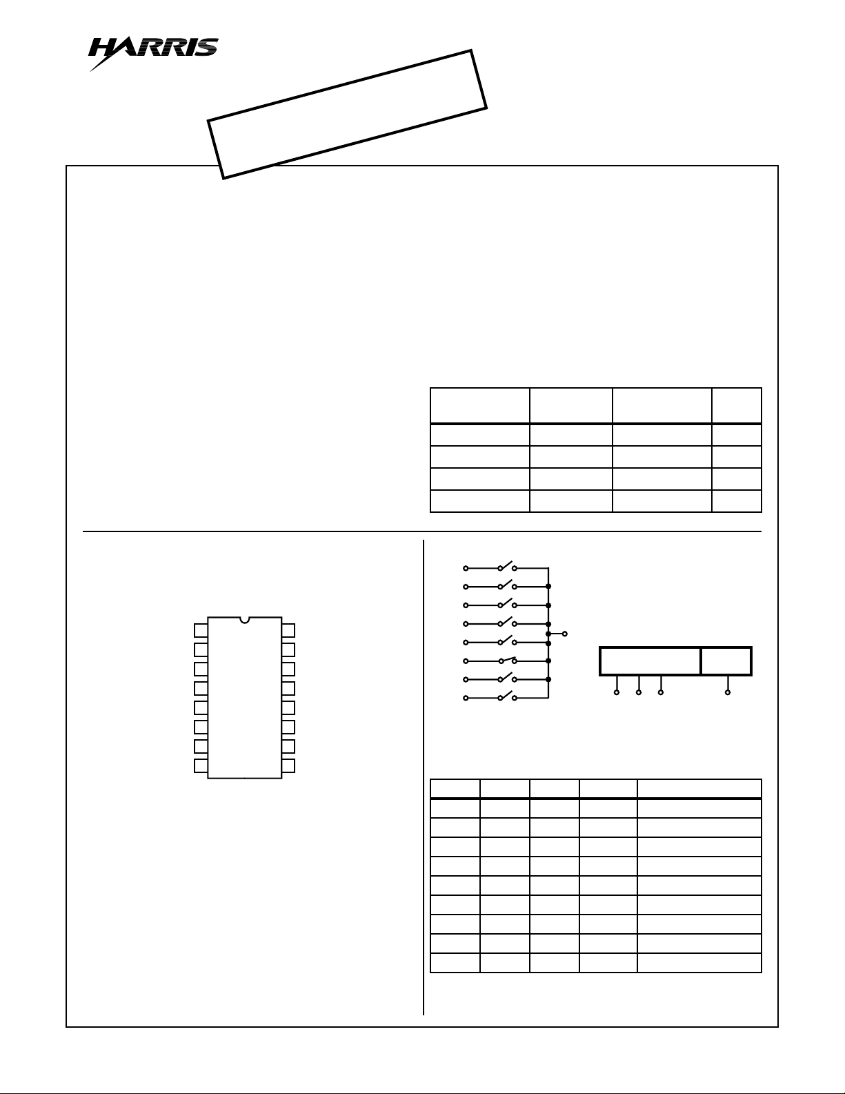
The IH6108 is a CMOS 1-of-8 multiplexer. The part is a plugin replacement for the DG508A. Three-line decoding is used
so that the 8 channels can be controlled by 3 Address
inputs; additionally a fourth input is provided for use as a
system enable. When the ENABLE input is high (5V), a
channel is selected by the three Address inputs, and when
low (0V) all channels are off. The 3 Address inputs are TTL
and CMOS logic compatible, with a “1” corresponding to any
voltage greater than 2.4V.
Part Number Information
PART
NUMBER
IH6108MJE -55 to 125 16 Ld CERDIP F16.3
IH6108MJE/883B -55 to 125 16 Ld CERDIP F16.3
IH6108CJE 0 to 70 16 Ld CERDIP F16.3
IH6108CPE 0 to 70 16 Ld PDIP E16.3
TEMP.
RANGE (oC) PACKAGE
PKG.
NO.
Pinout
(CERDIP, PDIP)
1
A
0
2
EN
3
V-
S
4
1
5
S
2
6
S
3
7
S
4
8
D
IH6108
TOP VIEW
Functional Diagram
S
1
S
2
S
3
S
16
A
1
15
A
2
14
GND
V+
13
12
S
5
11
S
6
10
S
7
9
S
8
4
S
5
S
6
S
7
S
8
A
2
x x x 0 None
000 1 1
001 1 2
010 1 3
011 1 4
100 1 5
101 1 6
110 1 7
111 1 8
NOTE: A0, A1, A
A
1
Logic “1” = VAH≥ 2.4V, V
Logic “0” = VAL≤ 0.8V.
2
V
OUT
D
3 LINE BINARY ADDRESS INPUT
TRUTH TABLE
A
0
EN ON SWITCH
ENH
ADDRESS DECODER
1 OF 8
A0A1A
ABOVE EXAMPLE SHOWS
CHANNEL 6 TURNED ON.
≥ 4.5V
2
(1 0 1) AND EN AT 5V
ENABLE
INPUT
EN
CAUTION: These devices are sensitive to electrostatic discharge. Users should follow proper IC Handling Procedures.
Copyright
© Harris Corporation 1997
12-128
File Number 3156.2

IH6108
Absolute Maximum Ratings Thermal Information
VIN (A, EN) to Ground . . . . . . . . . . . . . . . . . . . . . . . . . . -15V to 15V
VS or VD to V+ . . . . . . . . . . . . . . . . . . . . . . . . . . . . . . . . . . .0V, -36V
VS to VD to V-. . . . . . . . . . . . . . . . . . . . . . . . . . . . . . . . . . . . 0V, 36V
V+ to Ground . . . . . . . . . . . . . . . . . . . . . . . . . . . . . . . . . . . . . . . 18V
V- to Ground. . . . . . . . . . . . . . . . . . . . . . . . . . . . . . . . . . . . . . . .-18V
Current (Any Terminal) . . . . . . . . . . . . . . . . . . . . . . . . . . . . . . 30mA
Current (Analog Source or Drain) . . . . . . . . . . . . . . . . . . . . . .20mA
Operating Conditions
Temperature Range
C Suffix . . . . . . . . . . . . . . . . . . . . . . . . . . . . . . . . . . . .0oC to 70oC
M Suffix. . . . . . . . . . . . . . . . . . . . . . . . . . . . . . . . .-55oC to 125oC
CAUTION: Stresses above those listed in “Absolute Maximum Ratings” may cause permanent damage to the device. This is a stress only rating and operation
of the device at these or any other conditions above those indicated in the operational sections of this specification is not implied.
NOTE:
1. θJA is measured with the component mounted on an evaluation PC board in free air.
CAUTION: Stresses above those listed in “Absolute Maxim um Ratings” ma y cause permanent damage to the device . This is a stress only rating and oper ation of
the device at these or any other conditions above those indicated in the operational sections of this specification is not implied.
Thermal Resistance (Typical, Note 1) θJA (oC/W) θJC (oC/W)
PDIP Package. . . . . . . . . . . . . . . . . . . 100 N/A
CERDIP Package . . . . . . . . . . . . . . . . 75 20
Maximum Junction Temperature (Hermetic Package) . . . . . . . .175oC
Maximum Junction Temperature (Plastic Package) . . . . . . . . 150oC
Maximum Storage Temperature Range . . . . . . . . . .-65oC to 150oC
Maximum Lead Temperature (Soldering 10s). . . . . . . . . . . . . 300oC
Electrical Specifications V+ = 15V, V- = -15V, V
NO
TESTS
PARAMETER
SWITCH
r
DS(ON)
∆r
DS(ON)
I
S(OFF)
I
D(OFF)
I
D(ON)
INPUT
I
or I
AN(ON)
I
AN(OFF)IA(off)
I
A
A(on)
MEASURED
TERMINAL
S to D 8 180 VD= +10V, IS = -1.0mA
S 8 0.002 VS = 10V, VD = -10V - ±0.5 ±50 - ±1 ±50 nA
D 1 0.03 VD = 10V, VS = -10V,
D 8 0.1 V
A0, A1, or A
Inputs
A0, A1, A
EN 1 0.01 V
PER
TEMP
TYP
25oC TEST CONDITIONS
8 150 V
20 ∆r
8 0.002 V
1 0.03 V
8 0.1 V
3 0.01 VA = 0V - -10 -30 - -10 -30 µA
2
2
3 0.01 VA = 14V - 10 30 - 10 30 µA
3 0.01 VEN = 5V, All VA = 0V
= +5V, Ground = 0V, Unless Otherwise Specified, (Note 4)
EN
M SUFFIX (oC) C SUFFIX (oC)
300 300 400 350 350 450 Ω
Sequence Each Switch On
VAL = 0.8V, VAH = 2.4V
= -10V, IS = -1.0mA
D
300 300 400 350 350 450 Ω
Sequence Each Switch On
VAL = 0.8V, VAH = 2.4V
=
DS(ON)
r
DS ON()MAXrDS ON()MIN
---------------------------------------------------------------------------------- -
–
r
DS ON()AVG
˙
------ %
,
VS = ±10V
= -10V, VD = 10V,
S
- ±0.5 ±50 - ±1 ±50 nA
VEN = 0.8V
- ±2 ±100 - ±5 ±100 nA
VEN = 0.8V
= -10V, VS = 10V,
D
- ±2 ±100 - ±5 ±100 nA
VEN = 0.8V
S(ALL)
= VD = 10V,
- ±2 ±100 - ±5 ±100 nA
Sequence Each Switch On
VAL = 0.8V, VAH = 2.4V
S(ALL)
= VD = -10V,
- ±2 ±100 - ±5 ±100 nA
Sequence Each Switch On
VAL = 0.8V, VAH = 2.4V
- -10 -30 - -10 -30 µA
(Address Pins)
= 0V, All VA = 0V
EN
- -10 -30 - -10 -30 µA
(Address Pins)
UNITS-55 25 125 0 25 70
12-129

IH6108
Electrical Specifications V+ = 15V, V- = -15V, V
EN
NO
TESTS
PARAMETER
MEASURED
TERMINAL
PER
TEMP
TYP
25oC TEST CONDITIONS
DYNAMIC
t
TRANSITION
t
OPEN
t
ON(EN)
t
OFF(EN)
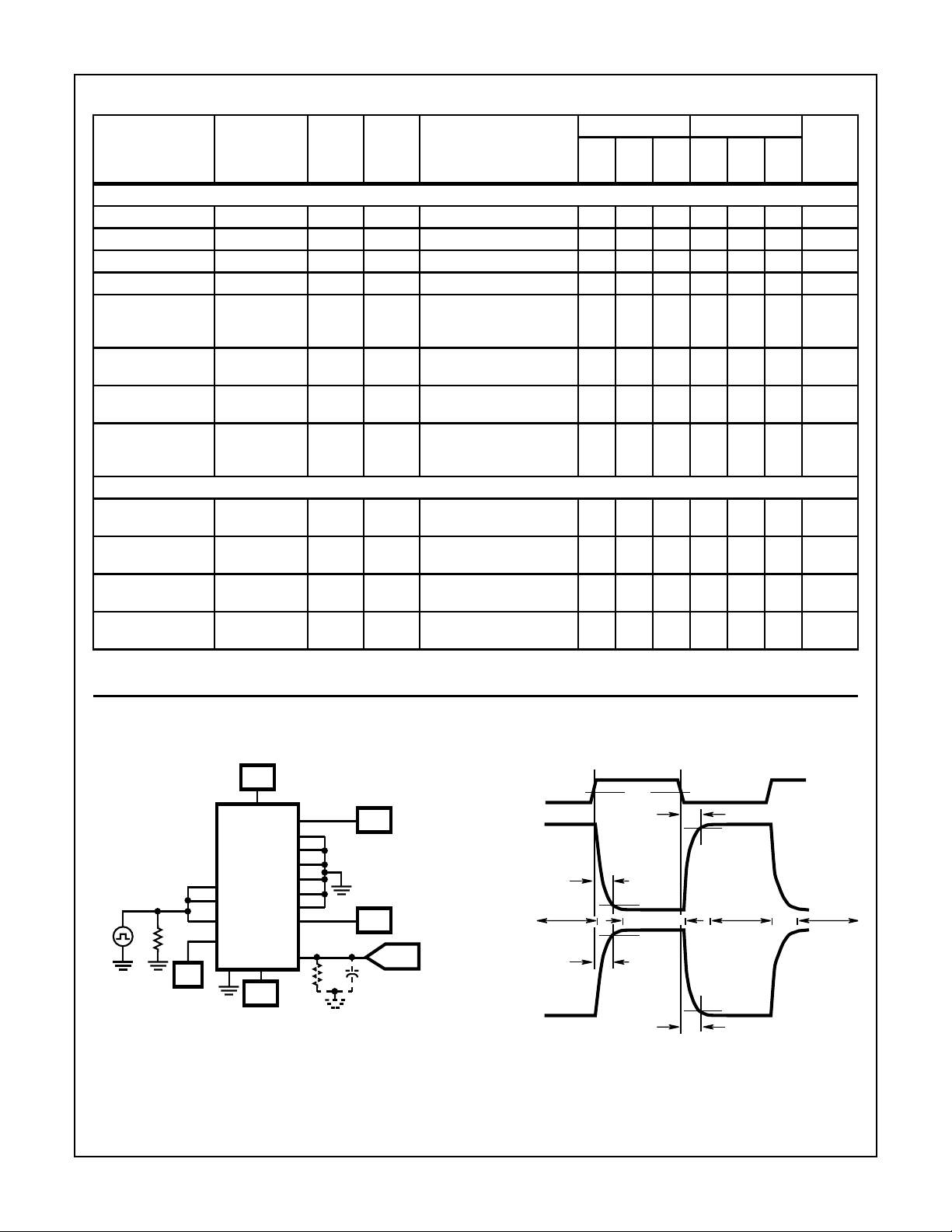
D 0.3 See Figure 1 - 1 ---- µs
D 0.2 See Figure 2 ------ µs
D 0.6 See Figure 3 - 1.5 ---- µs
D 0.4 See Figure 3 - 1 ---- µs
“OFF” Isolation D 60 V
C
S(OFF)
C
D(OFF)
C
DS(OFF)
S5V
D25V
D to S 1 VS = 0V, VD = 0V,
SUPPLY
Positive Supply
V+ 1 40 V
Current
Negative Supply
V- 1 2 V
Current
Positive Standby
V+ 1 1 V
Current
Negative Standby
V- 1 1 V
Current
NOTE:
2. See “Enable Input Strobing Levels”, in Application Section.
= +5V, Ground = 0V, Unless Otherwise Specified, (Note 4) (Continued)
M SUFFIX (oC) C SUFFIX (oC)
= 0V, RL = 200Ω,
EN
CL = 3pF, VS = 3V
RMS
------ dB
,
f = 500kHz
= 0V, VEN = 0V,
S
------ pF
f = 140kHz to 1MHz
= 0V,VEN= 0V,
D
------ pF
f = 140kHz to 1MHz
------ pF
VEN = 0V,
f = 140kHz to 1MHz
EN
= 5V,
- - 200 - - 1000 µA
All VA = 0V or 5V
EN
= 5V,
- - 100 - - 1000 µA
All VA = 0V or 5V
EN
= 0V,
- - 100 - - 1000 µA
All VA = 0V or 5V
EN
= 0V,
- - 100 - - 1000 µA
All VA = 0V or 5V
UNITS-55 25 125 0 25 70
Switching Information
+15V
V+
IH6108
A
0
A
1
A
V
A
50Ω
+5V
2
EN
V-GND
-15V
FIGURE 1. t
+10V
-10V
3V
50%0.8V
t
trans
S8 ON
t
trans
-9V
+9V
(1-8)
(1-8)
-10V
+10V
t
trans
+9V
S1 ON
-9V
t
trans
(8-1)
S8 ON
(8-1)
V
A
tr < 100ns
tf < 100ns
S
1
S
2
S
3
S
4
S
5
S
6
S
7
S
8
V
OUT
D
±10V
±10V
C
R
P
P
PROBE IMPEDANCE
TRANSITION
V
OUT
VS1 = +10V
VS8 = -10V
S1 ON
PROBE
V
OUT
VS1 = -10V
V
= +10V
R
P
C
P
≥ 1MΩ
≤ 30pF
S8
SWITCHING TEST CIRCUIT AND WAVEFORMS
12-130
 Loading...