Intersil Corporation ICM7249 Datasheet

August 1997
ICM7249
51/2 Digit LCD,
Micro-Power Event/Hour Meter
Features
• Hour Meter Requires Only 4 Parts Total
• Micropower Operation: < 1µA at 2.8V (Typ)
1
• 10 Year Operation On One Lithium Cell. 2
/2 Year
Battery Life with Display Connected
• Directly Drives 5
1
/2 Digit LCD
• 14 Programmable Modes of Operation
• Times Hrs., 0.1 Hrs., 0.01 Hrs., 0.1 Mins.
• Counts 1’s, 10’s, 100’s, 1000’s
• Dual Function Input Circuit
- Selectable Debounce for Counter
- High-Pass Filter for Timer
• Direct AC Line Triggering with Input Resistor
• Winking “Timer Active” Display Output
• Display Test Feature
Applications
• AC or DC Hour Meters
• AC or DC Totalizers
• Portable Battery Powered Equipment
• Long Range Service Meters
Ordering Information
TEMP.
PART NUMBER
ICM7249IPM -20 to 85 48 Ld PDIP E48.6
RANGE (oC) PACKAGE
PKG.
NO.
Description
The ICM7249 Timer/Counter is intended for long-term
battery-supported industrial applications. The ICM7249
typically draws 1µA during active timing or counting, due to
Intersil’ special low-power design techniques. This allows
more than 10 years of continuous operation without battery
replacement. The chip offers four timing modes, eight
counting modes and four test modes.
The ICM7249 is a 48 lead device, powered by a single DC
voltage source and controlled by a 32.768kHz quartz crystal.
No other external components are required. Inputs to the
chip are TTL-compatible and outputs drive standard direct
drive LCD segments.
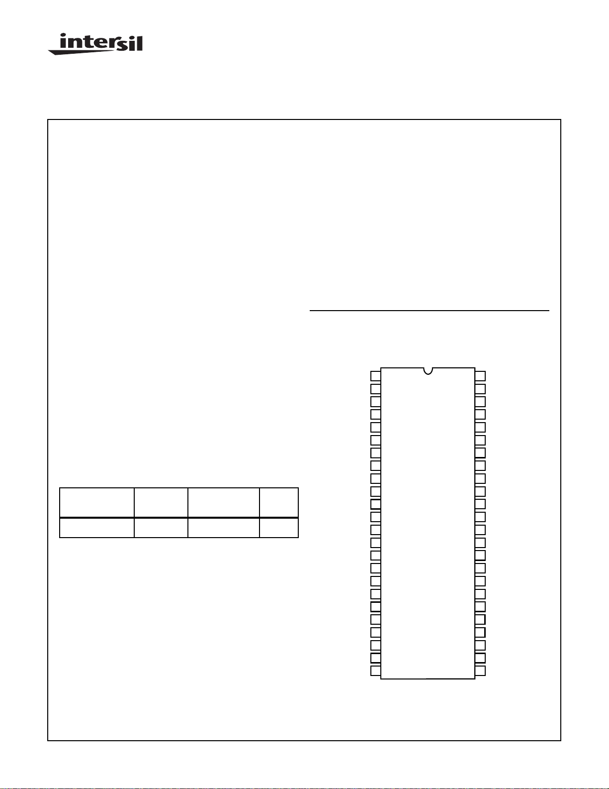
Pinout
ICM7249
(PDIP)
TOP VIEW
b6/c6
g5
e5
d5
c5
b5
a5
g4
e4
d4
c4
b4
a4
g3
e3
d3
c3
b3
a3
g2
1
f5
2
3
4
5
6
7
8
f4
9
10
11
12
13
14
15
f3
16
17
18
19
20
21
22
23
f2
24
48
DT
S/S
47
C3
46
C2
45
C1
44
C0
43
GND
42
OSC OUTPUT
41
OSC INPUT
40
V
39
DD
BP
38
W
37
a1
36
b1
35
c1
34
d1
33
e1
32
g1
31
f1
30
a2
29
b2
28
c2
27
d2
26
e2
25
CAUTION: These devices are sensitive to electrostatic discharge; follow proper IC Handling Procedures.
http://www.intersil.com or 407-727-9207
| Copyright © Intersil Corporation 1999
9-23
File Number 3170.1

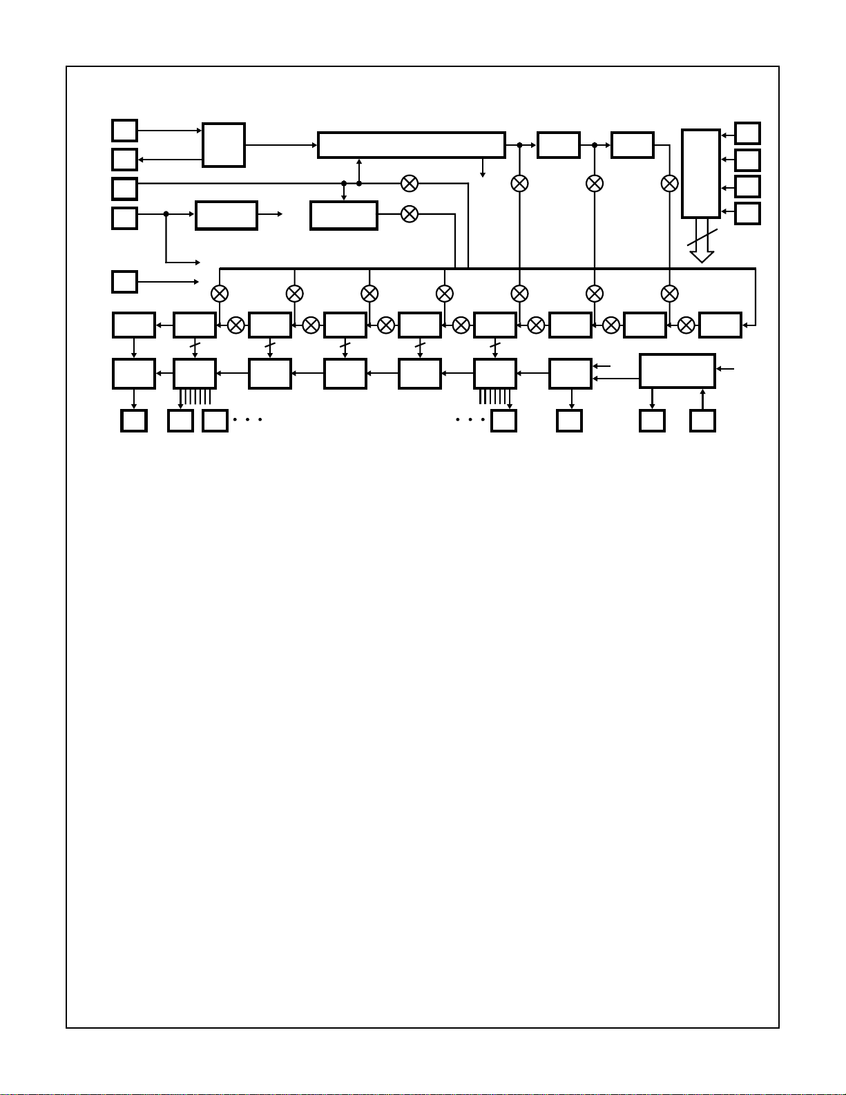
Functional Block Diagram
ICM7249
OSC
OSC
OUT
6 SEC1Hz
IN
S/S
V+
V-
2
÷
1 SEG
DEC
B6 F5 G5 A1 W BP DT
OSC
VOLTAGE
REGLATOR
10
÷
44
7 SEG
DEC
10
÷
7 SEG
DEC
SWITCH
DEBOUNCE
÷
7 SEG
DEC
10
215DIVIDER
10
÷
7 SEG
DEC
32Hz
÷
7 SEG
DEC
6
÷
10
10
÷
WINK
SEG
÷
1Hz
6
÷
10
DISPLAY
TEST
DECODE
CONTROL
16
÷
C0
C1
C2
C3
10
32Hz
9-24

ICM7249
Absolute Maximum Ratings Thermal Information
Supply Voltage (VDD - VSS). . . . . . . . . . . . . . . . . . . . . . . . . . . . . 6V
Input Voltage, Pins 43 - 48 (Note 1) . . (VSS- 0.3V) to (VDD+ 0.3V)
Operating Conditions
Temperature Range . . . . . . . . . . . . . . . . . . . . . . . . . . -40oC to 85oC
CAUTION: Stresses above those listed in “Absolute Maximum Ratings” may cause permanent damage to the device. This is a stress only rating and operation
of the device at these or any other conditions above those indicated in the operational sections of this specification is not implied.
NOTES:
1. Due to the SCR structure inherent in junction-isolated CMOS devices. the circuit can be put in a latchup mode it large currents are injected
into device inputs or outputs. For this reason special care should be taken in a system with multiple power supplies to prevent voltages
being applied to inputs or outputs before power is applied. If only inputs are aff ected, latchup also can be prev ented by limiting the current
into the input terminal to less than 1mA.
2. θJA is measured with the component mounted on an evaluation PC board in free air.
Thermal Resistance (Typical, Note 2) θJA (oC/W)
PDIP Package. . . . . . . . . . . . . . . . . . . . . . . . . . . . . 50
Maximum Junction Temperature. . . . . . . . . . . . . . . . . . . . . . . 150oC
Maximum Storage Temperature Range . . . . . . . . . .-65oC to 150oC
Maximum Lead Temperature (Soldering, 10s) . . . . . . . . . . . . 300oC
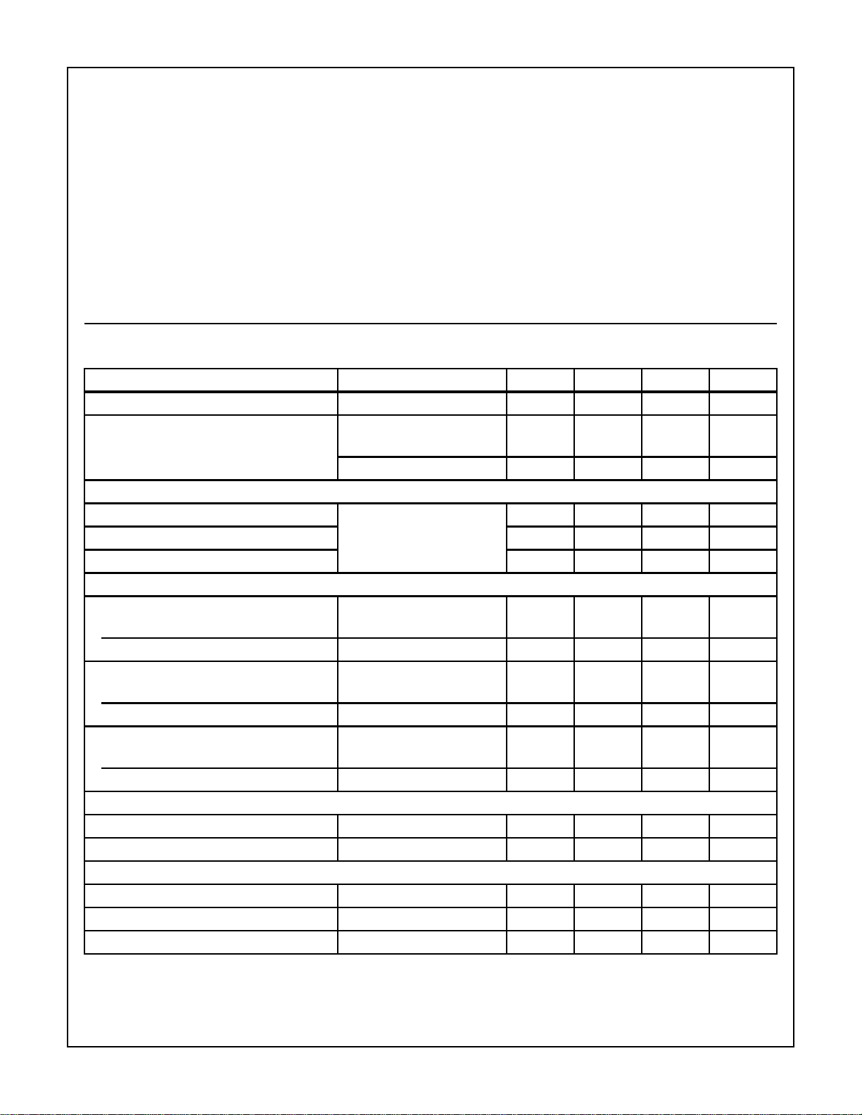
Electrical Specifications Temperature = -40
o
C to 85oC, VDD = 2.5V to 5.5V, VSS = 0V, Unless Otherwise Specified. Typical
Specifications Measured at Temperature = 25oC and VDD = 2.8V, Unless Otherwise Specified
PARAMETER TEST CONDITIONS MIN TYP MAX UNITS
Operating Voltage, V
Operating Current, I
DD
DD
Note 1 2.5 - 5.5 V
All Inputs = VDD or GND, Note 2
= 2.8V - 1.0 10.0 µA
V
DD
VDD = 5.5V - 4.0 20.0 µA
INPUT CURRENT
C0 - C3, I
S/S, I
SS
DT, I
DT
IN
All Inputs VDD or GND
VDD = 2.8V
Note 3
0.0 - 1 µA
0.5 1.5 3.0 µA
40.0 - 110 µA
INPUT VOLTAGE
C0 - C3, DT, S/S
V
IL
V
IH
- - 0.3V
0.7V
DD
--V
DD
V
Segment Output Voltage
V
OL
V
OH
IOL = 1µA - - 0.8 V
IOH = 1µAV
- 0.8 - - V
DD
Backplane Output Voltage
V
OL
V
OH
IOL = 10µA - - 0.8 V
IOH = 10µAV
- 0.8 - - V
DD
OSCILLATOR STABILITY
Temperature = 25oC, VDD = 2.5V to 5.5V - 0.1 - ppm
Temperature = -40oC to 85oC, VDD = 2.5V to 5.5V - 5 - ppm
S/S PULSE WIDTH
High-Pass Filter (Modes 0 - 3), t
Debounce (Modes 4, 6, 8, 10), t
HP
DE
Without Debounce (Modes 5, 7, 9, 11), t
DE
5 - 10,000 µs
10,000 - - µs
5--µs
NOTES:
1. Internal reset to 00000 requires a maximum VDD rise time of 1µs. Longer rise times at power-up may cause improper reset.
2. Operating current is measured with the LCD disconnected, and input current ISS and IDT supplied externally.
3. Inputs C0 - C3 are latched internally and draw no DC current after switching. During switching, a 90µA peak current ma y be dra wn f or 10ns.
9-25
 Loading...