Intersil Corporation ICM7243 Datasheet

August 1997
ICM7243
8-Character, Microprocessor-
Compatible, LED Display Decoder Driver
Features
• 14-Segment and 16-Segment Fonts with Decimal Point
• Mask Programmable for Other Font-Sets Up to 64
Characters
• Microprocessor Compatible
• Directly Drives LED Common Cathode Displays
• Cascadable Without Additional Hardware
• Standby Feature Turns Display Off; Puts Chip in Low
Power Mode
• Sequential Entry or Random Entry of Data Into
Display
• Single +5V Operation
• Character and Segment Drivers, All MUX Scan
Circuitry, 8 x 6 Static Memory and 64-Character ASCll
Font Generator Included On-Chip
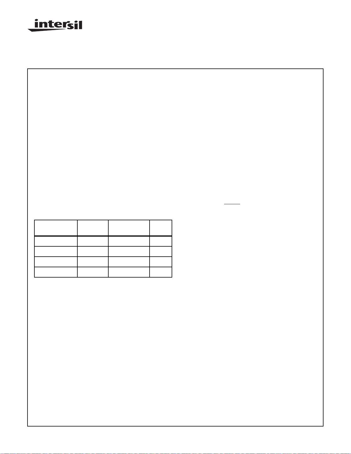
Ordering Information
TEMP.
PART NUMBER
ICM7243AIJL -25oC to 85 40 Ld CERPDIP F40.6
ICM7243AIPL -25oC to 85 40 Ld PDIP E40.6
ICM7243BIJL -25oC to 85 40 Ld CERPDIP F40.6
RANGE (oC) PACKAGE
PKG.
NO.
Description
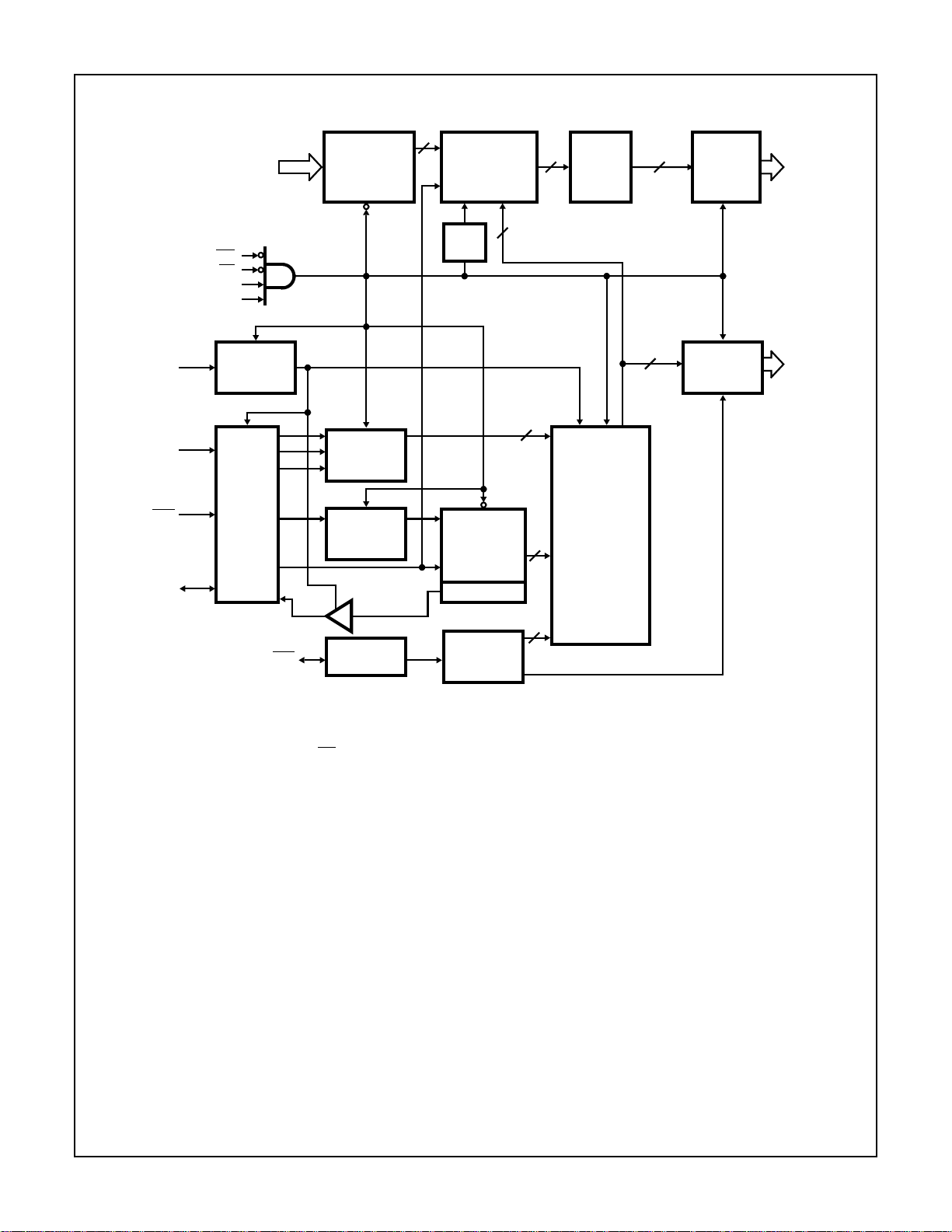
The ICM7243 is an 8-character, alphanumeric display driver
and controller which provides all the circuitry required to
interface a microprocessor or digital system to a 14-segment
or 16-segment display. It is primarily intended for use in
microprocessor systems, where it minimizes hardware and
software overhead. Incorporated on-chip are a 64-character
ASClI decoder, 8 x 6 memory, high power character and
segment drivers, and the multiplex scan circuitry.
6-bit ASCll data to be displayed is written into the memory
directly from the microprocessor data bus. Data location
depends upon the selection of either Sequential
(MODE = 1) or Random access mode (MODE = 0). In the
Sequential Access mode the first entry is stored in the
lowest location and displayed in the “left-most” character
position. Each subsequent entry is automatically stored in
the next higher location and displayed to the immediate
“right” of the previous entry. A DISPlay FULL signal is provided after 8 entries; this signal can be used for cascading
devices together. A
ory and reset the location counter. The Random Access
mode allows the processor to select the memory address
and display digit for each input word.
The character multiplex scan runs whenever data is not
being entered. It scans the memory and CHARacter drivers,
and ensures that the decoding from memory to display is
done in the proper sequence. Intercharacter blanking is
provided to avoid display ghosting.
CLeaR pin is provided to clear the mem-
ICM7243BlPL -25 to 85 40 Ld PDIP E40.6
CAUTION: These devices are sensitive to electrostatic discharge; follow proper IC Handling Procedures.
http://www.intersil.com or 407-727-9207
| Copyright © Intersil Corporation 1999
9-21
File Number 3162.1

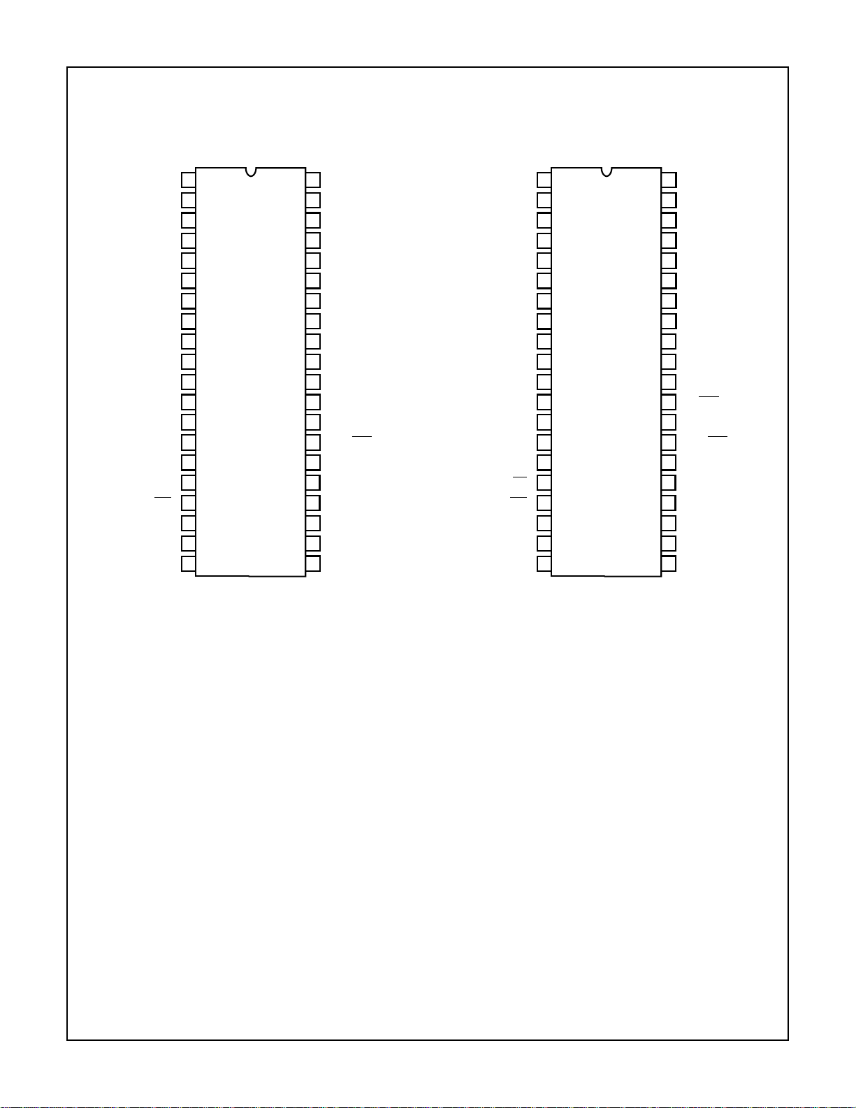
Pinouts
ICM7243
ICM7243A (16-SEGMENT CHARACTER)
(PDIP, CERDIP)
TOP VIEW
V
DD
SEG m
SEG e
SEG g1
SEG k
SEG c
SEG d1
SEG a1
SEG a2
D0
D1
D2
D3
D4
D5
CS
WR
CHAR 8
CHAR 7
CHAR 6
1
2
3
4
5
6
7
8
9
10
11
12
13
14
15
16
17
18
19
20
40
39
38
37
36
35
34
33
32
31
30
29
28
27
26
25
24
23
22
21
SEG
l
SEG g2
SEG b
SEG i
SEG f
SEG d2
DP
SEG
h
SEG j
MODE
A0/SEN
A1/CLR
A2/DISP FULL
OSC/
OFF
CHAR 1
CHAR 2
CHAR 3
CHAR 4
V
SS
CHAR 5
ICM7243B (14-SEGMENT CHARACTER)
(PDIP, CERDIP)
TOP VIEW
V
DD
SEG e
SEG g1
SEG k
SEG c
SEG d
SEG a
D0
D1
D2
D3
D4
D5
CS
CS
CS
WR
CHAR 8
CHAR 7
CHAR 6
1
2
3
4
5
6
7
8
9
10
11
12
13
14
15
16
17
18
19
20
40
39
38
37
36
35
34
33
32
31
30
29
28
27
26
25
24
23
22
21
SEG
m
SEG l
SEG g2
SEG b
SEG i
SEG f
DP
SEG
h
SEG j
MODE
A0/SEN
CLR
A1/
A2/DISP FULL
OSC/
OFF
CHAR 1
CHAR 2
CHAR 3
CHAR 4
V
SS
CHAR 5
9-22

Functional Block Diagram
ICM7243
(NOTE 1)
MODE
A0/SEN
CLR
A1/
A2/DISP FULL
DATA INPUT
D0 - D5
WR
CS
CS
CS
CL
D
SEL
MUX
DAT A
D
LATCHES
CL
CL
D
ADDRESS
LATCHES
CL
D
CONTROL
LATCH
Q
Q
8 x 6
D1
DAT A
MEMORY
CLR
CLR
ADR
CL
ONE
SHOT
CL
EN
SEQUENTIAL
SEQUENTIAL
ADDRESS
COUNTER
OVERFLOW
D0
8
3
3
ROM
(NOTE 1)
SEL
ADDRESS
MULITPLEXER
MULTIPLEXER
AND
DECODER
64 x 17
6
17
(NOTE 1)
8
SEGMENT
DRIVERS
8
CHARACTER
CHARACTER
DRIVERS
SEGMENT
OUTPUTS
SEG x
CHAR N
CHARACTER
OUTPUTS
OFF
OSC/
NOTE:
1. ICM7243A has only one CS and no CS.
ICM7243B has 15 Segments.
OSCILLATOR
MULTIPLEX
OSCILLATOR
CHARACTER
MULTIPLEX
COUNTER
3
INTER-CHARACTER BLANKING
9-23

ICM7243
Absolute Maximum Ratings Thermal Information
Supply Voltage VDD - VSS . . . . . . . . . . . . . . . . . . . . . . . . . . . .+6.0V
Input Voltage (Any Terminal) . . . . . . . . . . . VDD +0.3V to VSS -0.3V
CHARacter Output Current. . . . . . . . . . . . . . . . . . . . . . . . . . .300mA
SEGment Output Current. . . . . . . . . . . . . . . . . . . . . . . . . . . . .30mA
Operating Conditions
Temperature Range . . . . . . . . . . . . . . . . . . . . . . . . . . -25oC to 85oC
CAUTION: Stresses above those listed in “Absolute Maximum Ratings” may cause permanent damage to the device. This is a stress only rating and operation
of the device at these or any other conditions above those indicated in the operational sections of this specification is not implied.
NOTE:
1. θJA is measured with the component mounted on an evaluation PC board in free air.
Thermal Resistance (Typical, Note 1) θJA (oC/W) θJC (oC/W)
PDIP Package. . . . . . . . . . . . . . . . . . . 55 N/A
CERDIP Package . . . . . . . . . . . . . . . . 50 10
Maximum Junction Temperature
CERDIP Package . . . . . . . . . . . . . . . . . . . . . . . . . . . . . . . . 175oC
PDIP Package. . . . . . . . . . . . . . . . . . . . . . . . . . . . . . . . . . . 150oC
Maximum Storage Temperature Range . . . . . . . . . .-65oC to 150oC
Maximum Lead Temperature (Soldering 10s). . . . . . . . . . . . . 300oC
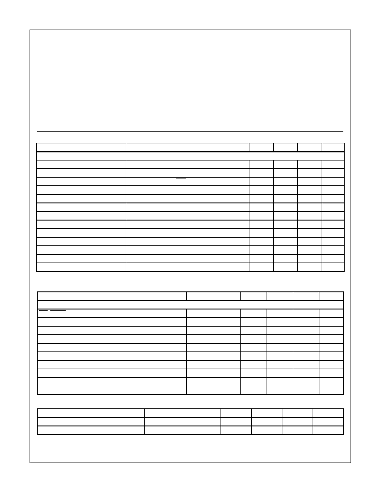
Electrical Specifications V
= 5V, VSS = 0V, TA = 25oC, Unless Otherwise Specified
DD
PARAMETER TEST CONDITIONS MIN TYP MAX UNITS
DC CHARACTERISTICS
IN
- VSS), V
DD
IH
IL
DS
DD
STBY
CHAR
SEG
SUPP
CHLK
SLK
OL
OH
V
= 5.25V, 10 Segments ON, All 8 Characters - 180 - mA
SUPP
V
= 5.25V, OSC/OFF Pin < 0.5V, CS = V
SUPP
V
SUPP
V
SUPP
= 5V, V
= 5V, V
= 1V 140 190 - mA
OUT
= 2.5V 14 19 - mA
OUT
SS
IOL = 1.6mA - - 0.4 V
lIH = 100µA 2.4 - - V
Supply Voltage (V
Operating Supply Current, I
Quiescent Supply Current, I
Input High Voltage, V
Input Low Voltage, V
Input Current, I
CHARacter Drive Current, I
CHARacter Leakage Current, I
SEGment Drive Current, I
SEGment Leakage Current, I
DISPlay FULL Output Low, V
DISPlay FULL Output High, V
Display Scan Rate, f
Electrical Specifications Drive levels 0.4V and 2.4V, timing measured at 0.8V and 2.0V. V
Specified
PARAMETER TEST CONDITIONS MIN TYP MAX UNITS
AC CHARACTERISTICS
WR, CLeaR Pulse Width Low, t
WPI
WR, CLeaR Pulse Width High (Note 1), t
Data Hold Time, t
Data Setup Time, t
Address Hold Time, t
Address Setup Time, t
CS Setup Time, t
CS,
Pulse Transition Time, t
SEN Setup Time, t
Display Full Delay, t
DH
DS
AH
AS
CS
T
SEN
WDF
WPH
300 250 - ns
250 150 - ns
125 - - ns
700 480 - ns
4.75 5.0 5.25 V
- 30 250 µA
2- -V
- - 0.8 V
-10 - +10 µA
- - 100 µA
- 0.01 10 µA
- 400 - Hz
= 5V, TA = 25oC, Unless Otherwise
DD
- 250 - ns
0 -100 - ns
40 15 - ns
0--ns
- - 100 ns
0 -25 - ns
Capacitance
PARAMETER TEST CONDITIONS MIN TYP MAX UNITS
Input Capacitance, C
Output Capacitance, C
NOTES:
1. In Sequential mode
2. For design reference only, not tested.
lN
O
WR high must be ≥ T
(Note 2) - 5 - pF
(Note 2) - 5 - pF
+T
WDF
.
SEN
9-24
 Loading...