August 1997
ICM7226A,
ICM7226B
8-Digit, Multi-Function,
Frequency Counter/Timer
Features
• CMOS Design for Very Low Power
• Output Drivers Directly Drive Both Digits and
Segments of Large 8-Digit LED Displays
• Measures Frequencies from DC to 10MHz; Periods
from 0.5µs to 10s
• Stable High Frequency Oscillator uses either 1MHz or
10MHz Crystal
• Both Common Anode and Common Cathode Available
• Control Signals Available for External Systems
Interfacing
• Multiplexed BCD Outputs
Applications
• Frequency Counter
• Period Counter
• Unit Counter
• Frequency Ratio Counter
• Time Interval Counter
Ordering Information
TEMP.
PART NUMBER
ICM7226AlJL -25 to 85 40 Ld CERDIP F40.6
ICM7226BlPL -25 to 85 40 Ld PDIP E40.6
RANGE (oC) PACKAGE
PKG.
NO.
Description
The ICM7226 is a fully integrated Universal Counter and
LED display driver. It combines a high frequency oscillator, a
decade timebase counter, an 8-decade data counter and
latches, a 7-segment decoder, digit multiplexer and segment
and digit drivers which can directly drive large LED displays.
The counter inputs accept a maximum frequency of 10MHz
in frequency and unit counter modes and 2MHz in the other
modes. Both inputs are digital inputs. In many applications,
amplification and level shifting will be required to obtain
proper digital signals for these inputs.
The ICM7226 can function as a frequency counter, period
counter, frequency ratio (f
or as a totalizing counter. The devices require either a
10MHz or 1MHz quartz crystal timebase, or if desired an
external timebase can also be used. For period and time
interval, the 10MHz timebase gives a 0.1µs resolution. In
period average and time interval average, the resolution can
be in the nanosecond range. In the frequency mode, the
user can select accumulation times of 0.01s, 0.1s, 1s and
10s. With a 10s accumulation time, the frequency can be displayed to a resolution of 0.1Hz. There is 0.2s between measurements in all ranges. Control signals are provided to
enable gating and storing of prescaler data.
Leading zero blanking has been incorporated with frequency
display in kHz and time in µs. The display is multiplexed at a
500Hz rate with a 12.2% duty cycle for each digit. The
ICM7226A is designed for common anode displays with typical peak segment currents of 25mA, and the ICM7226B is
designed for common cathode displays with typical segment
currents of 12mA. In the display off mode, both digit drivers
and segment drivers are turned off, allowing the display to
be used for other functions.
) counter, time interval counter
A/fB
CAUTION: These devices are sensitive to electrostatic discharge; follow proper IC Handling Procedures.
http://www.intersil.com or 407-727-9207
| Copyright © Intersil Corporation 1999
9-15
File Number 3169.1

ICM7226A, ICM7226B
Pinouts
CONTROL INPUT
INPUT B
MEASUREMENT IN PROGRESS
FUNCTION
STORE
BCD 4
BCD 8
DP
SEG
SEG g
SEG a
V
SEG d
SEG b
SEG c
SEG f
BCD 2
BCD 1
RST INPUT
EXT DP IN
ICM7226A
COMMON ANODE (CERDIP)
TOP VIEW
1
2
3
4
5
6
7
8
e
9
10
11
12
SS
13
14
15
16
17
18
19
20
40
INPUT A
39
HOLD
38
BUF OSC OUT
37
NC (NOTE 1)
36
OSC OUT
35
OSC IN
34
NC (NOTE 1)
33
EXT OSC IN
32
RST OUT
31
EXT RANGE
D1
30
D2
29
D3
28
D4
27
D5
26
V
25
DD
24
D6
23
D7
22
D8
21
RANGE
COMMON CATHODE (PDIP)
BCD 4
BCD 8
D1
D3
D2
D4
V
D5
D6
D7
D8
BCD 2
BCD 1
SS
1
2
3
4
5
6
7
8
9
10
11
12
13
14
15
16
17
18
19
20
CONTROL INPUT
INPUT B
MEASUREMENT IN PROGRESS
FUNCTION
STORE
RST INPUT
EXT DP IN
NOTE:
1. For maximum frequency stability, connect to VDD or VSS.
ICM7226B
TOP VIEW
40
INPUT A
39
HOLD
38
BUF OSC OUT
37
NC (NOTE 1)
36
OSC OUT
35
OSC IN
34
NC (NOTE 1)
33
EXT OSC IN
32
RST OUT
31
EXT RANGE
DP OUT
30
SEG
29
SEG
28
SEG a
27
SEG d
26
V
25
DD
24
SEG b
23
SEG c
22
SEG f
21
RANGE
g
e
9-16

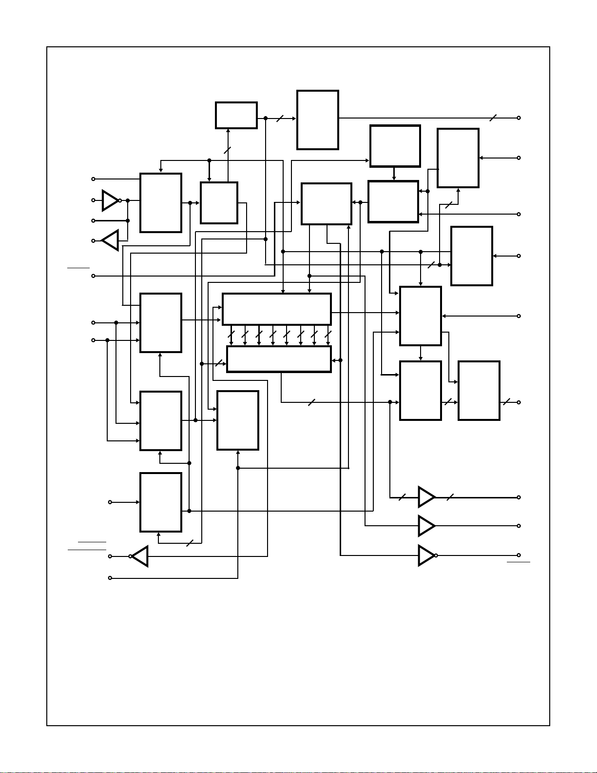
Functional Block Diagram
EXT OSC
INPUT
OSC
INPUT
OSC
OUTPUT
BUF OSC
OUTPUT
RESET
INPUT
OSC
SELECT
DECODER
3
104 OR
5
10
ICM7226A, ICM7226B
8
100Hz
DIGIT
DRIVERS
STORE
AND RESET
LOGIC
REFERENCE
COUNTER
3
+10
RANGE
SELECT
LOGIC
6
RANGE
CONTROL
LOGIC
5
CONTROL
LOGIC
DIGIT
OUTPUTS
8
RANGE
INPUT
EXT RANGE
INPUT
CONTROL
INPUT
(8)
INPUT A
INPUT B
FUNCTION
INPUT
MEAS IN
PROGRESS
OUTPUT
HOLD
INPUT
INPUT
CONTROL
LOGIC
INPUT
CONTROL
LOGIC
FN
CONTROL
LOGIC
MAIN
EN
COUNTER
3
÷10
CL
44444444
8
D
CL
6
DATA LATCHES
OUTPUT MUX
Q
MAIN
FF
R
RESET
OVERFLOW
STORE
478
DP
LOGIC
DECODER
AND LZB
LOGIC
4 4
SEGMENT
DRIVERS
EXT
DP
INPUT
SEGMENT
OUTPUTS
(8)
BCD
OUTPUTS
(4)
RESET
OUTPUT
STORE
OUTPUT
9-17

ICM7226A, ICM7226B
Absolute Maximum Ratings Thermal Information
Maximum Supply Voltage (VDD - VSS). . . . . . . . . . . . . . . . . . . .6.5V
Maximum Digit Output Current. . . . . . . . . . . . . . . . . . . . . . . .400mA
Maximum Segment Output Current . . . . . . . . . . . . . . . . . . . . .60mA
Voltage On Any Input or
Output Terminal (Note 1) . . . . . . . . . . . . . . VDD +0.3V to VSS -0.3V
Operating Conditions
Temperature Range . . . . . . . . . . . . . . . . . . . . . . . . . . -25oC to 85oC
CAUTION: Stresses above those listed in “Absolute Maximum Ratings” may cause permanent damage to the device. This is a stress only rating and operation
of the device at these or any other conditions above those indicated in the operational sections of this specification is not implied.
NOTES:
1. Destructive latchup may occur if input signals are applied bef ore the po w er supply is estab lished or if inputs or outputs are f orced to
voltages exceeding VDD or VSS by 0.3V.
2. θJA is measured with the component mounted on an evaluation PC board in free air.
Thermal Resistance (Typical, Note 2) θJA (oC/W) θJC (oC/W)
CERDIP Package . . . . . . . . . . . . . . . . 45 9
PDIP Package. . . . . . . . . . . . . . . . . . . 50 N/A
Maximum Junction Temperature
CERDIP Package . . . . . . . . . . . . . . . . . . . . . . . . . . . . . . . . 175oC
PDIP Package. . . . . . . . . . . . . . . . . . . . . . . . . . . . . . . . . . . 150oC
Maximum Storage Temperature Range . . . . . . . . . .-55oC to 150oC
Maximum Lead Temperature (Soldering 10s). . . . . . . . . . . . .300oC
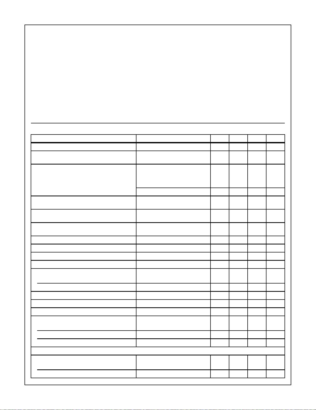
Electrical Specifications V
= 5.0V, TA = 25oC, Unless Otherwise Specified
DD
PARAMETER TEST CONDITIONS MIN TYP MAX UNITS
Operating Supply Current, I
Supply Voltage Range (V
Maximum Frequency INPUT A, Pin 40, f
Maximum Frequency INPUT B, Pin 2, f
DD
-VSS), V
DD
SUPPLY
A(MAX)
B(MAX)
Minimum Separation INPUT A to INPUT B,
Time Interval Function
Oscillator Frequency and External Oscillator Frequency,
f
OSC
Oscillator Transconductance, g
Multiplex Frequency, f
MUX
M
Time Between Measurements f
Input Rate of Charge, dV
/dt Inputs A, B - 15 - mV/µs
IN
Input Voltages: Pins 2, 19, 33, 39, 40, 35
Input Low Voltage, V
Input High Voltage, V
Pins 2, 39, 40, Input Leakage, A, B, I
Input Resistance to V
Input Resistance to V
IL
lH
Pins 19, 33, R
DD
Pin 31, R
SS
ILK
IN
IN
Output Current
Low Output Current, Pins 3, 5-7, 17, 18, 32, 38, I
High Output Current, Pins 5-7, 17, 18, 32, H
High Output Current, Pins 3, 38, H
OL
OLVOL
OL
ICM7226A
Segment Driver: Pins 8-11, 13-16
Low Output Current, I
High Output Current, I
OL
OH
Display Off, Unused Inputs to V
-25oC to 85oC, INPUT A,
INPUT B Frequency at f
MAX
-25oC to 85oC
SS
-25mA
4.75 - 6.0 V
10 14 - MHz
4.75V < VDD < 6.0V, Figure 9
Function = Frequency, Ratio,
Unit Counter
Function = Period, Time Interval 2.5 - - MHz
-25oC to 85oC
2.5 - - MHz
4.75V < VDD < 6.0V, Figure 10
o
-25
C to 85oC
250 - - ns
4.75V < VDD < 6.0V, Figure 1
-25oC to 85oC
0.1 - 10 MHz
4.75V < VDD < 6.0V
VDD -4.75V, TA = 85oC 2000 - - µS
f
= 10MHz - 500 - Hz
OSC
= 10MHz - 200 - ms
OSC
-25oC to 85oC - - 1.0 V
3.5 - - V
--20µA
VIN = VDD -1.0V 100 400 - kΩ
VIN = +1.0V 50 100 - kΩ
= +0.4V 400 - - µA
VOH = +2.4V 100 - - µA
VOH = VDD -0.8V 265 - - µA
VO = +1.5V 25 35 - mA
VO = VDD -1.0V - 100 - µA
9-18

ICM7226A, ICM7226B
Electrical Specifications V
= 5.0V, TA = 25oC, Unless Otherwise Specified (Continued)
DD
PARAMETER TEST CONDITIONS MIN TYP MAX UNITS
Multiplex Inputs: Pins 1, 4, 20, 21
Input Low Voltage, V
Input High Voltage, V
Input Resistance to V
IL
IH
SS,RIN
VIN = +1.0V 50 100 - kΩ
Digit Driver: Pins 22-24, 26-30
Low Output Current, I
High Output Current, I
OL
OH
VO = +1.0V - -0.3 - mA
VO = VDD -2.0V 150 180 - mA
ICM7226B
Segment Driver: Pins 22-24, 26-30
Leakage Current, I
L
High Output Current, I
OH
VO = V
SS
VO = VDD -2.0V 10 15 - mA
Multiplex Inputs: Pins 1, 4, 20, 21
Input Low Voltage, V
Input High Voltage, V
Input Resistance to V
IL
IH
SS,RIN
VIN = VDD -1.0V 100 360 - kΩ
Digit Driver: Pins 8-11, 13-16
Low Output Current, I
High Output Current, I
OL
OH
VO = +1.0V 50 75 - mA
VO = VDD -2.5V - 100 - µA
NOTES:
1. Assumes all leads soldered or welded to PC board and free air flow.
2. Typical values are not tested.
- - 0.8 V
2.0 - - V
--10µA
--V
-2.0 V
DD
VDD-0.8 - - V
Timing Waveform
40ms
STORE
30ms TO 40ms
RESET
UPDATE
190ms TO 200ms
MEASUREMENT
IN PROGRESS
INPUT A
INPUT B
NOTE:
1. If range is set to 1 event, first and last measured interval will coincide.
FIGURE 1. WAVEFORMS FOR TIME INTERVAL MEASUREMENT (OTHERS ARE SIMILAR, BUT WITHOUT PRIMING PHASE)
60ms
40ms
FUNCTION:
TIME INTERVAL
PRIMING
PRIMING EDGES
MEASUREMENT INTERVAL
250ns MIN
MEASURED
INTERVAL
(FIRST)
MEASURED
INTERVAL
(LAST)
UPDATE
9-19

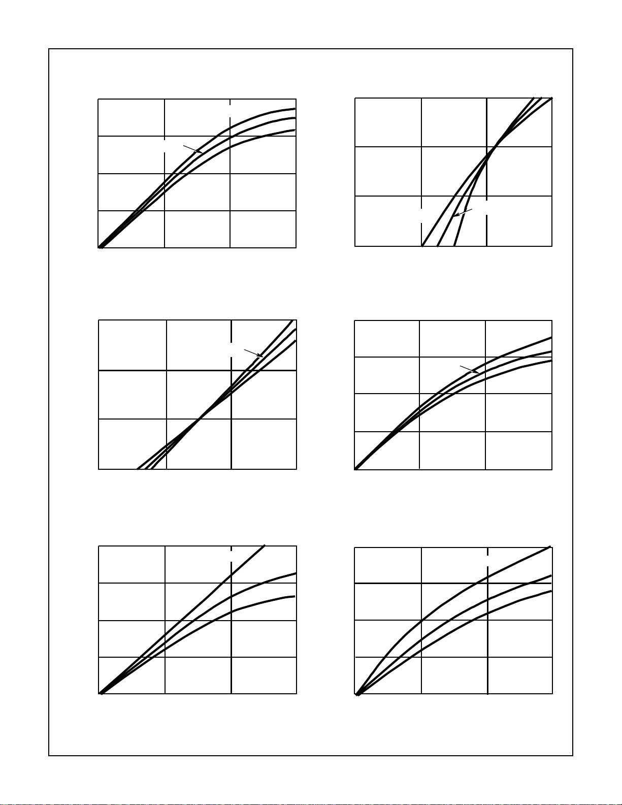
Typical Performance Curves
ICM7226A, ICM7226B
200
TA = 25oC
50
(mA)
100
DIGIT
I
50
0
01 2 3
VDD = 5.0V
V
OUT
FIGURE 2. ICM7226B TYPICAL I
30
4.5 ≤ VDD≤ 6.0V
20
(mA)
SEG
I
10
(V)
VDD = 5.5V
VDD = 4.5V
vs V
DIGIT
25oC
OUT
-20oC
85oC
300
4.5 ≤ VDD≤ 6.0V
200
(mA)
DIG
I
100
85oC
0
0
123
FIGURE 3. ICM7226A TYPICAL I
80
TA = 25oC
(mA)
SEG
I
60
40
20
VDD = 5.0V
V
DD-VOUT
-20oC
(V)
DIG
25oC
vs VDD-V
VDD = 5.5V
VDD = 4.5V
OUT
0
0 123
DD-VOUT
V
(V)
OUT
(V)
SEG
DIGIT
vs VDD-V
-20oC
vs V
OUT
25oC
85oC
OUT
V
FIGURE 4. ICM7226B TYPICAL I
200
VDD = 5.0V
150
(mA)
100
DIGIT
I
50
0
0 123
FIGURE 6. ICM7226B TYPICAL I
0
01 2 3
V
(V)
OUT
FIGURE 5. ICM7226A TYPICAL I
80
VDD = 5.0V
60
(mA)
40
SEG
I
20
0
0 123
(V)
V
OUT
FIGURE 7. ICM7226A TYPICAL I
SEG
SEG
vs V
-20oC
vs V
OUT
25oC
85oC
OUT
9-20
 Loading...