ICM7224
August 1997
Features
• High Frequency Counting - Guaranteed 15MHz, Typically
25MHz at 5V
• Low Power Operation - Typically Less Than 100µW
Quiescent
•
STORE and RESET Inputs Permit Operation as
Frequency or Period Counter
• True
•
COUNT INHIBIT Disables First Counter Stage
CARRY Output for Cascading Four-Digit Blocks
• Schmitt-Trigger on the COUNT Input Allows Operation
in Noisy Environments or with Slowly Changing Inputs
• Leading Zero Blanking INput and OUTput for Correct
Leading Zero Blanking with Cascaded Devices
• Provides Complete Onboard Oscillator and Divider
Chain to Generate Backplane Frequency, or
Backplane Driver May be Disabled Allowing Segments
to be Slaved to a Master Backplane Signal
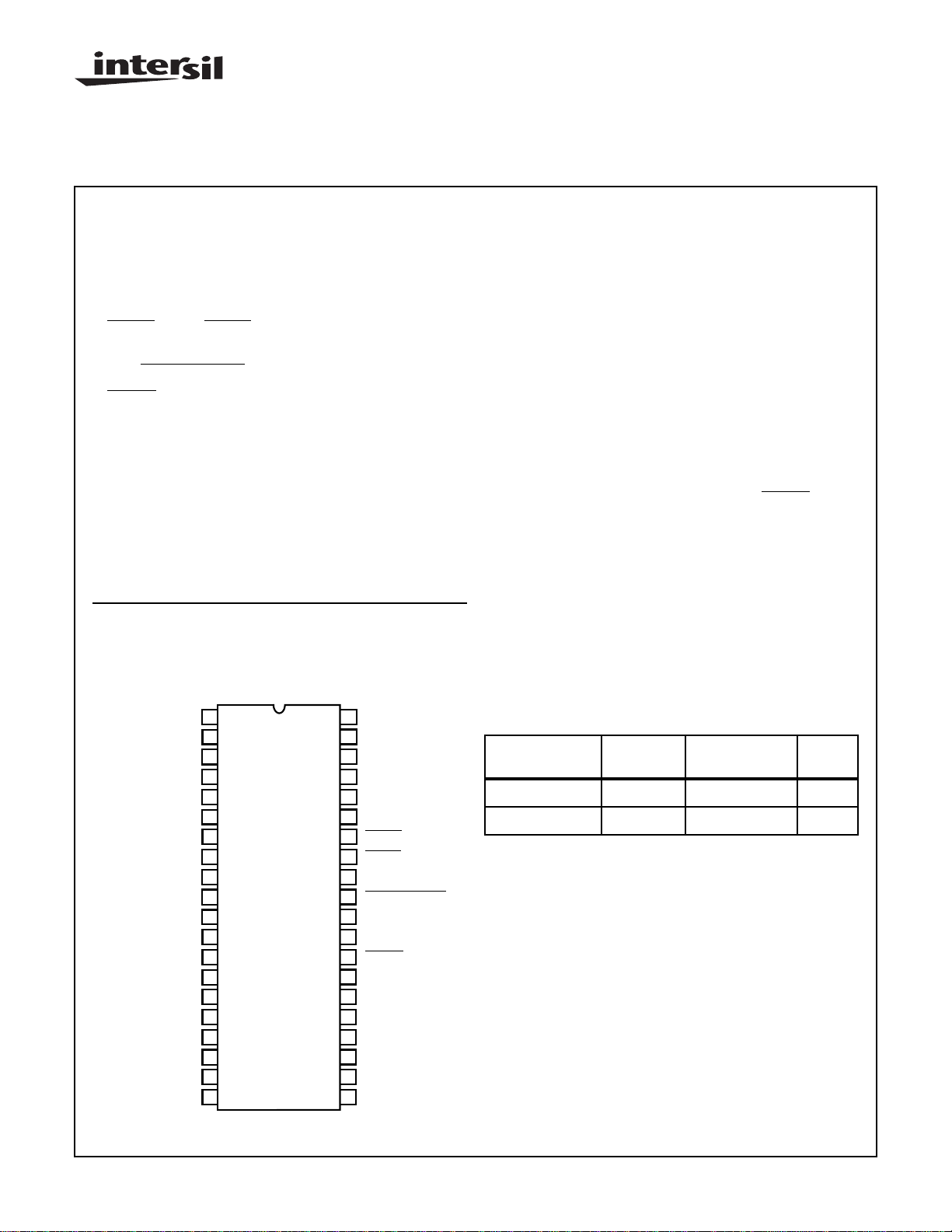
Pinout
ICM7224
(PDIP)
TOP VIEW
41/2 Digit LCD Display Counter
Description
The ICM7224 device is a high-performance, CMOS 41/
digit counter, including decoder, output latch, display driver,
count inhibit, leading zero blanking, and reset circuitry.
The counter section provides direct static counting, guaranteed from DC to 15MHz, using a 5V ±10% supply over the
operating temperature range. At normal ambient temperatures, the devices will typically count up to 25MHz. The
COUNT input is provided with a Schmitt trigger to allow
operation in noisy environments and correct counting with
slowly changing inputs. The COUNT INHIBIT, STORE and
RESET inputs allow a direct interface with the ICM7207 and
ICM7207A to implement a low cost, low power frequency
counter with a minimum component count.
These devices also incorporate several features intended to
simplify cascading four-digit blocks. The
allows the counter to be cascaded, while the Leading Zero
Blanking INput and OUTput allows correct Leading Zero
Blanking between four-decade blocks. The BackPlane driver
of the LCD devices may be disabled, allowing the segments
to be slaved to another backplane signal, necessary when
using an eight or twelve digit, single backplane display.
These devices provide maximum count of 19999. The
display drivers are not of the multiplexed type and each display segment has its own individual drive pin, providing high
quality display outputs.
CARRY output
2
1
V
DD
2
E1
3
G1
F1
4
5
BP
A2
6
7
B2
8
C2
D2
9
10
E2
G2
11
12
F2
A3
13
B3
14
15
C3
D3
16
17
E3
G3
18
F3
19
20
A4
40
D1
39
C1
38
B1
37
A1
36
OSCILLATOR
35
V
SS
STORE
34
RESET
33
COUNT
32
COUNT INHIBIT
31
LZB OUT
30
LZB IN
29
CARRY
28
1
/2 - DIGIT
27
F4
26
G4
25
E4
24
D4
23
C4
22
B4
21
Ordering Information
TEMP.
PART NUMBER
ICM7224IPL -25 to 85 40 Ld PDIP E40.6
ICM7224RIPL † -25 to 85 40 Ld PDIP E40.6
RANGE (oC) PACKAGE
† “R” Indicates Device With Reversed Leads Configuration.
PKG.
NO.
CAUTION: These devices are sensitive to electrostatic discharge; follow proper IC Handling Procedures.
http://www.intersil.com or 407-727-9207
| Copyright © Intersil Corporation 1999
9-14
File Number 3168.1

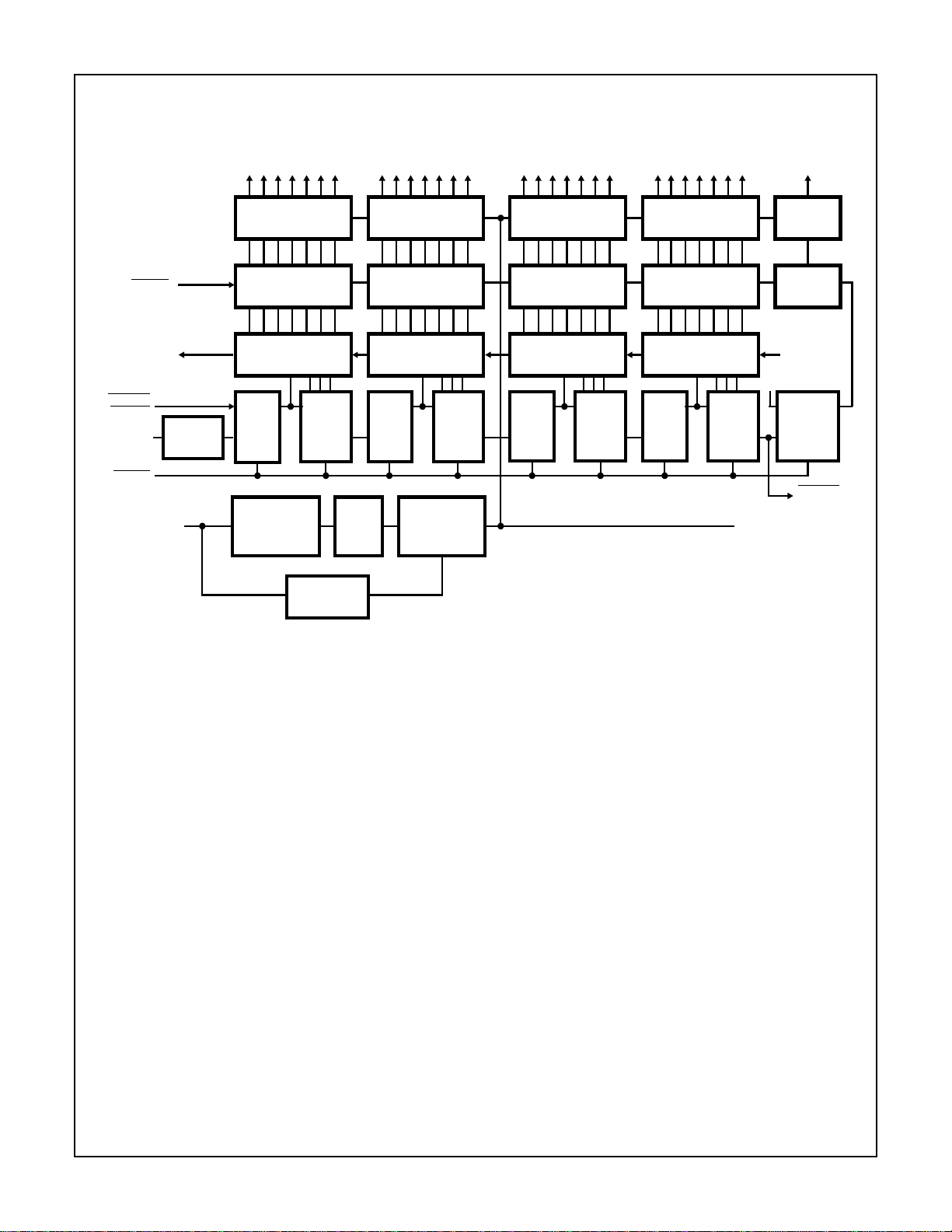
Functional Block Diagram
ICM7224
STORE
LEADING
ZERO
BLANKING
OUTPUT
COUNT
INHIBIT
COUNT
INPUT
RESET
OSCILLATOR
INPUT
SCHMITT
TRIGGER
LSD
DIGIT 1
SEGMENT OUTPUTS
7 WIDE DRIVER
7 WIDE LATCH
DECODER
CL
Q
2
÷
CL
R
OSCILLATOR
5
÷
Q
R
ENABLE
DETECTOR
DIGIT 2
SEGMENT OUTPUTS
7 WIDE DRIVER
7 WIDE LATCH
DECODER DECODER DECODER
Q
2
÷
CL
R
BLACKPLANE
+124
CL
÷
DRIVER
ENABLE
MSD
1
V
DD
D
CL
/2 DIGIT
OUTPUT
1
/2 DIGIT
DRIVER
1
/2 DIGIT
LATCH
LEADING
ZERO
BLANKING
INPUT
Q
1
/
2
DIGIT
R
CARRY
OUTPUT
DIGIT 3
SEGMENT OUTPUTS
7 WIDE DRIVER
7 WIDE LATCH
CL
Q
5
Q
R
CL
2
÷
R
5
÷
Q
R
DIGIT 4
SEGMENT OUTPUTS
7 WIDE DRIVER
7 WIDE LATCH
CL
Q
CL
2
÷
R
5
÷
Q
R
BP INPUT/OUTPUT
9-15

ICM7224
Absolute Maximum Ratings Thermal Information
Supply Voltage (VDD - VSS). . . . . . . . . . . . . . . . . . . . . . . . . . . .6.5V
Input Voltage (An y Terminal) (Note 1). . . .(VDD+ 0.3V) to (VSS- 0.3V)
Operating Conditions
Temperature Range . . . . . . . . . . . . . . . . . . . . . . . . . . -25oC to 85oC
CAUTION: Stresses above those listed in “Absolute Maximum Ratings” may cause permanent damage to the device. This is a stress only rating and operation
of the device at these or any other conditions above those indicated in the operational sections of this specification is not implied.
NOTES:
1. Due to the SCR structure inherent in the CMOS process, connecting any terminal to voltages greater than VDD or less than VSS may
cause destructive device latchup. For this reason, it is recommended that no inputs from sources operating on a different power supply
be applied to the device before its supply is established, and that in m ultiple supply systems, the supply to the ICM7224 be turned on first.
2. θJA is measured with the component mounted on an evaluation PC board in free air.
Thermal Resistance (Typical, Note 2) θJA (oC/W)
PDIP Package. . . . . . . . . . . . . . . . . . . . . . . . . . . . . 50
Maximum Junction Temperature . . . . . . . . . . . . . . . . . . . . . . .150oC
Maximum Storage Temperature Range . . . . . . . . . .-65oC to 150oC
Maximum Lead Temperature (Soldering, 10s) . . . . . . . . . . . .300oC
Electrical Specifications V
DD
PARAMETER TEST CONDITIONS MIN TYP MAX UNIT
Operating Current, I
DD
Operating Supply Voltage Range
(V
- V
SS
), V
SUPPLY
COUNT
IL
IH
OH
OL
OSC
BP
P
OSCI
, t
r
f
, t
r
f
CT
CH
DD
OSClLLATOR Input Current, I
Segment Rise/Fall Time, t
BackPlane Rise/Fall Time, t
Oscillator Frequency, f
Backplane Frequency, f
Input Pullup Currents, I
Input High Voltage, V
Input Low Voltage, V
COUNT Input Threshold, V
COUNT Input Hysteresis, V
Output High Current, I
Output Low Current, I
Count Frequency, f
STORE, RESET Minimum Pulse Width, tS, t
= 5V, VSS= 0V, TA = 25oC, Unless Otherwise Indicated
Test Circuit, Display Blank - 10 50 µA
Pin 36 - ±2 ±10 µA
C
= 200pF - 0.5 - µs
LOAD
C
= 5000pF - 1.5 - µs
LOAD
Pin 36 Floating - 19 - kHz
Pin 36 Floating - 150 - Hz
Pins 29, 31, 33, 34, VIN = VDD - 3V - 10 - µA
Pins 29, 31, 33, 34 3 - - V
Pins 29, 31, 33, 34 - - 1 V
CARRY Pin 28
-350 -500 - µA
Leading Zero Blanking OUT Pin 30
V
= VDD - 3V
OUT
CARRY Pin 28
350 500 - µA
Leading Zero Blanking OUT Pin 30
V
= +3V
OUT
4.5V < VDD < 6V 0 - 15 MHz
r
3-6V
-2-V
- 0.5 - V
3--µs
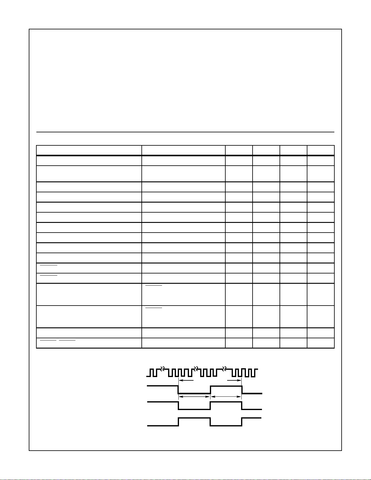
Timing Waveforms
OSCILLATOR
FREQUENCY
BACKPLANE
INPUT/OUTPUT
OFF SEGMENTS
ON SEGMENTS
FIGURE 1. ICM7224 DISPLAY WAVEFORMS
128 CYCLES
64 CYCLES
64 CYCLES
9-16
 Loading...